APB SP-308 1st Printing
APB - All Points Bulletin (rev 7) (Atari Games, 1987) · Schematic Package · 31 pages · 83 sections · original scan
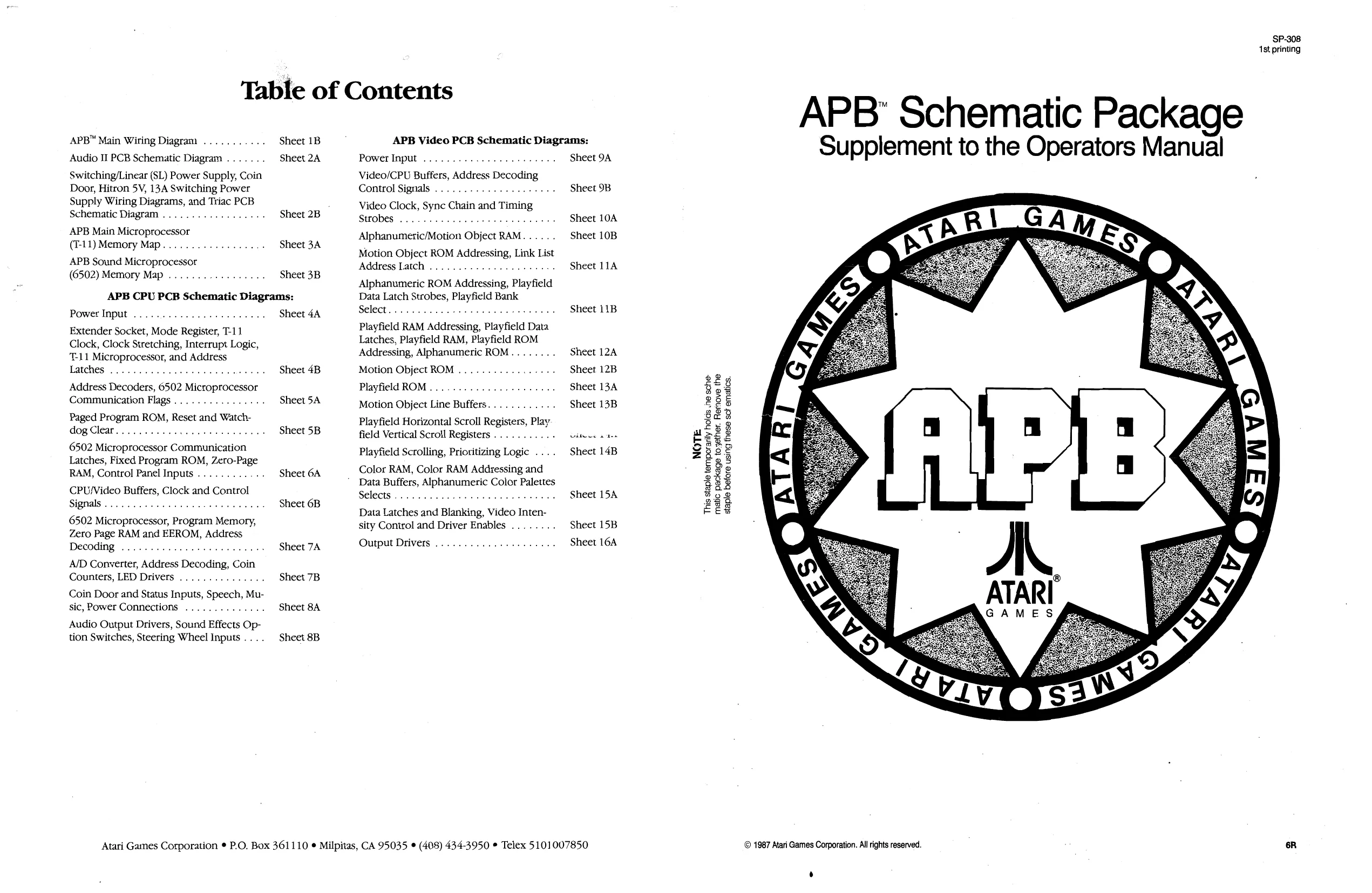
Table of Contents
APB™ Main Wiring Diagram ....... -.. Sheet 1B Audio II PCB Schematic Diagram ....... Sheet 2A. Switching/Linear (SL) Power Supply, Coin Door, Hitron 5V, 13A Switching Power Supply Wiring Diagrams, and Triac PCB Schematic Diagram ...............- . Sheet 2B APB Main Microprocessor (T-11) Memory Map...............- . Sheet 3A APB Sound Microprocessor (6502) Memory Map ............... . Sheet 3B
APB CPU PCB Schematic Diagrams: Power Input ........... 0.0000 eee eee Sheet 4A Extender Socket, Mode Register, T-11 Clock, Clock Stretching, Interrupt Logic, T11 Microprocessor, and Address Latches 20.6.0... cece eee eee Sheet 4B Address Decoders, 6502 Microprocessor Communication Flags.............+5. Sheet 5A Paged Program ROM, Reset and Watchdog Clear... cece eee cece ee Sheet 5B 6502 Microprocessor Communication Latches, Fixed Program ROM, Zero- Page RAM, Control Panel Inputs ............ Sheet 6A CPU/Video Buffers, Clock and Control Signals... 0.0... eee eee eee ... Sheet 6B 6502 Microprocessor, Program Memory, Zero Page RAM and EEROM, Address Decoding .............-0. eee eee Sheet 7A A/D Converter, Address Decoding, Coin Counters, LED Drivers ........... . Sheet 7B Coin Door and Status Inputs, Speech, M Mu-
sic, Power Connections .............. Sheet 8A Audio Output Drivers, Sound Effects Option Switches, Steering Wheel Inputs .... Sheet 8B APB Video PCB Schematic Diagrams: Power Input .............-. 0000000 Sheet 9A Video/CPU Buffers, Address ss Decoding Control Signals ..............0. 0000 Sheet 9B Video Clock, Syne Chain and Timing Strobes 6... 6.6 ee eee eee eee Sheet 10A Alphanumetie/Motion Object RAM. Sheet 10B Motion Object ROM Addressing, Link List Address Latch ..... : beet eee eee Sheet 11A Alphanumeric ROM Addressing, Playfield Data Latch Strobes, Playfield Bank Select... 0.6... cece eee eee eee Sheet 11B Playfield RAM Addressing, Playfield Data Latches, Playfield RAM, Playfield ROM Addressing, Alphanumeric ROM........ Sheet 12A Motion Object ROM ......-..-...0++5 Sheet 12B Playfield ROM Sheet 13A Motion Object Line Buffers Sheet 13B Playfield Horizontal Scroll Registers, Play field Vertical Scroll Registers : Playfield Scrolling, Prioritizing Logic .... Color RAM, Color RAM Addressing and Data Buffers, Alphanumeric Color Palettes SECC es ee ee we cee cee ee Sheet 15A Data Latches and Blanking, Video Intensity Control and Driver Enables ... . Sheet 15B eis @ gue gerne « greg Sheet 164 Sheet 14B
Output Drivers . .
Atari Games Corporation ® P.O, Box 361110 © Milpitas, CA 95035 ® (408) 434-3950 © Telex 5101007850
© 1987 Atari Games Corporation. All rights reserved. SP.308 1st printing
6R
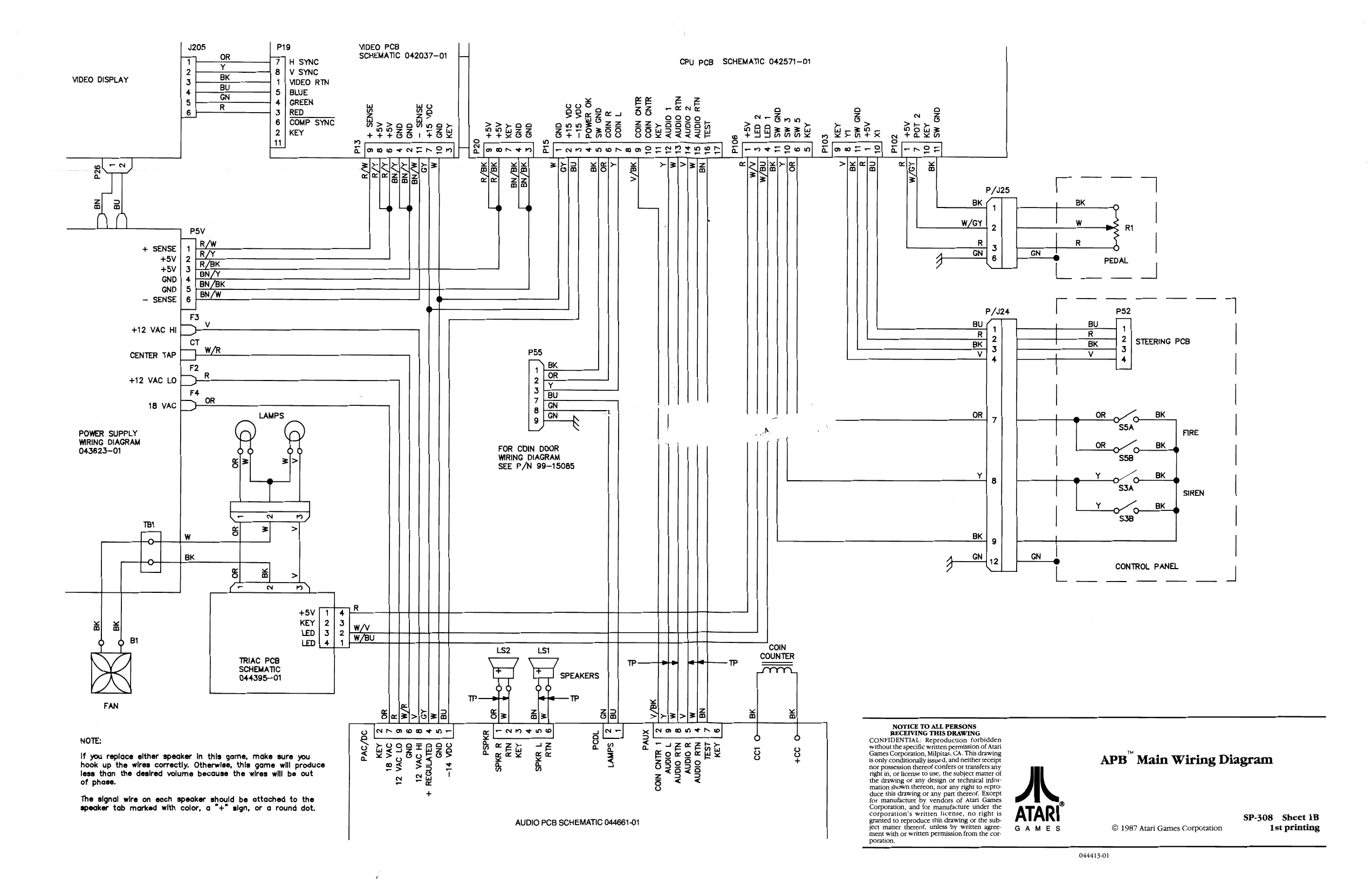
This page is a drawing, shown as the original scan.
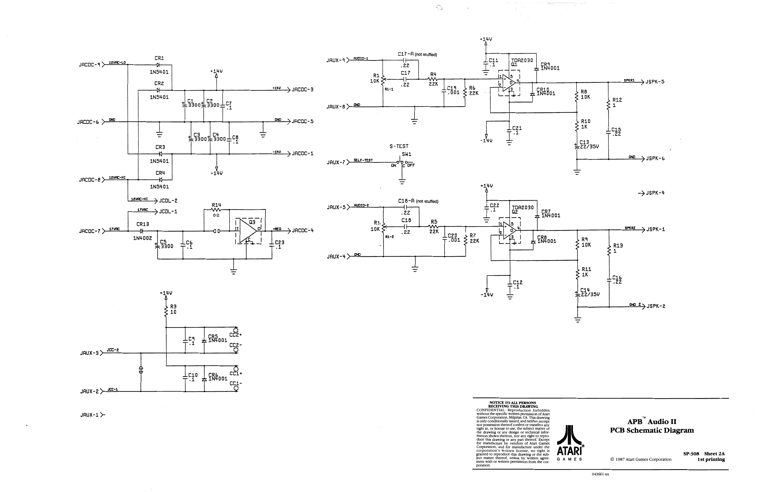
This page is a drawing, shown as the original scan.
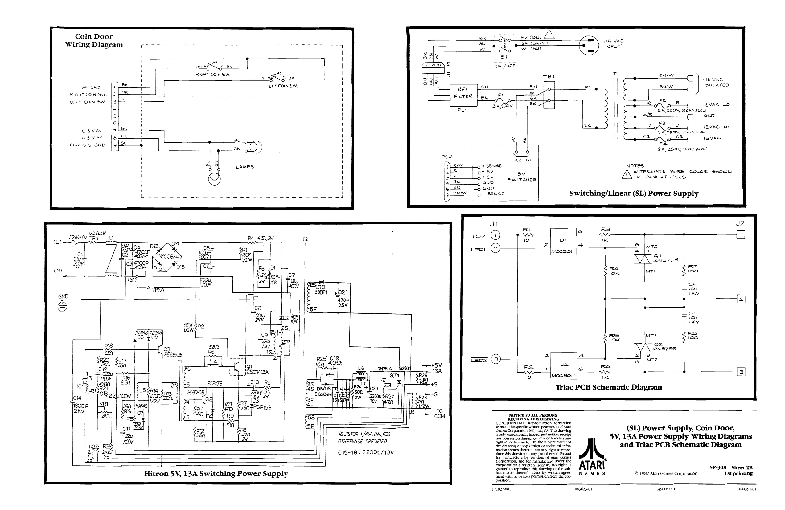
Coin Door
Wiring Diagram
RIGHT COIN SW. 115 VAC LEFT COINSW. | ent ISOLATED FILTER ow OND
RIGHT COIN SW
LEFT COIN SW KE Lo
Fu ND
v N2VAG HI 2Nesoy, stow-slow =J 1BvAc lo Ic G3 Vac
GBVAC
CHASSIS GND Ce ee
a lz
lo i e Fa 2A, 250V, Stow: BLOW
0 + SENSE NOTES o+ SV sv ALTERNATE WIRE COLOR SHOWN. +38 PAREN” . sv swirciier: IN PARENTHESES eND [6 eNo
- SENSE Switching/Linear (SL) Power Supply
uz
Moc 301 | Vi
Triac PCB Schematic Diagram
NOTICE TO ALL PERSONS RECEIVING THIS DRAWING CONFIDENTIAL: Reproduction forbidden Schhout the spetfic whiten pemission of Ata (SL) Power Supply, Coin Door, Bames Comeration Mipias CA thiodrrwing h > RESISTOR 1/4W, UNLESS isonly conditionally issued, and neither receipt, 5V, 13A Power Supply Wirin: Diagrams j noeposesion eet oni A f pply Wiring OTHERWISE SPECIFIED. Te dinwnng of any dean or eel infor MN and Triac PCB Schematic Diagram €15~18 : 2200u/10V Gace ts ruwing or tay part eae See for manufacture by vendors of Atari Games Gorporation and for manure under the AT, “ARI _ gamed ‘Siero is Sing eu SP-308 Sheet 2B Hitron 5V, 13A Switching Power Supply ject matter thereof, unless by written agree) GG AM ES © 1987 Atari Games Corporation Ist printing ‘ment with or written permission from the corporation. n t
171027-001 043623-01 149006-001 044395-01
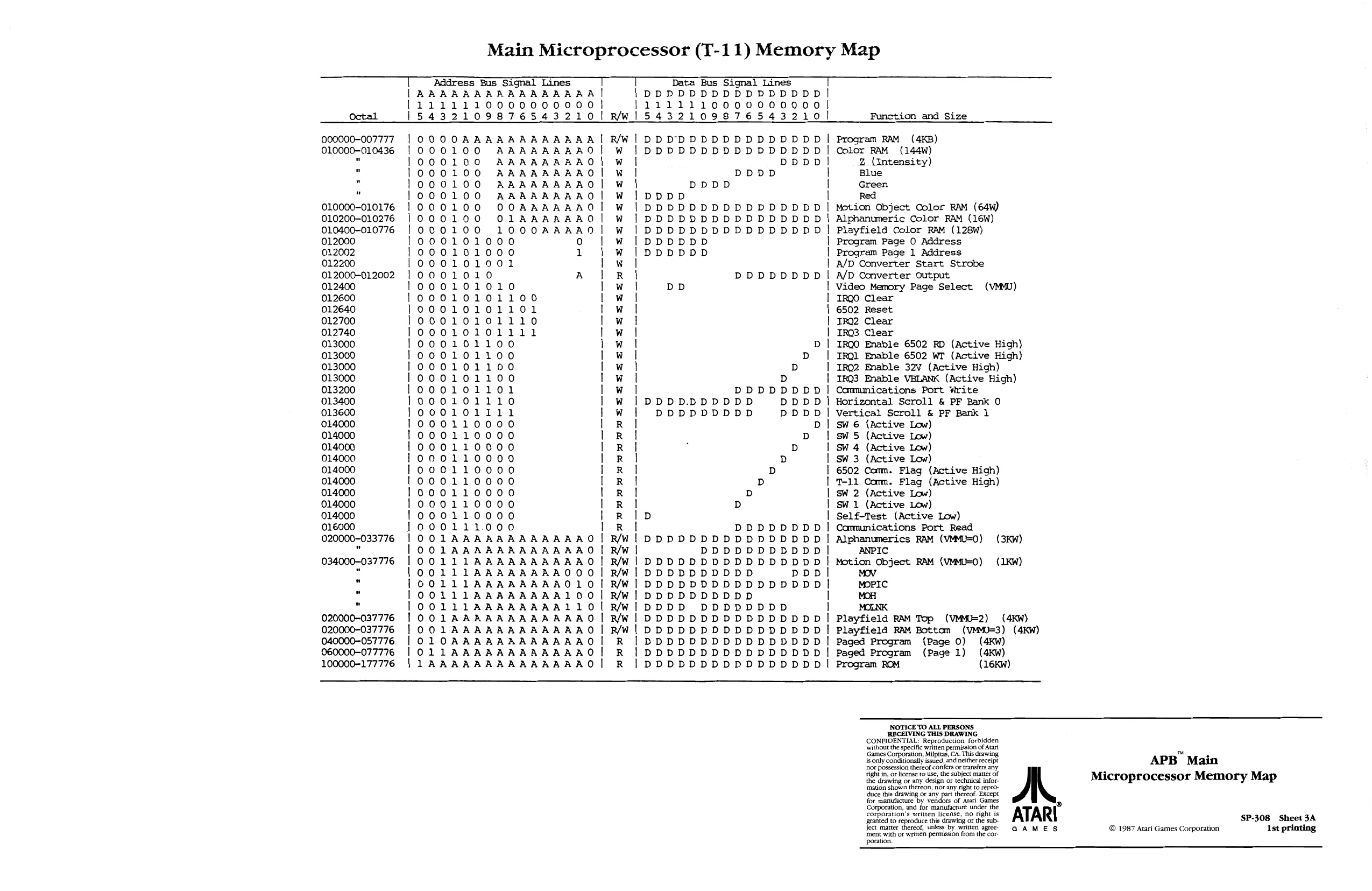
This page is a drawing, shown as the original scan.
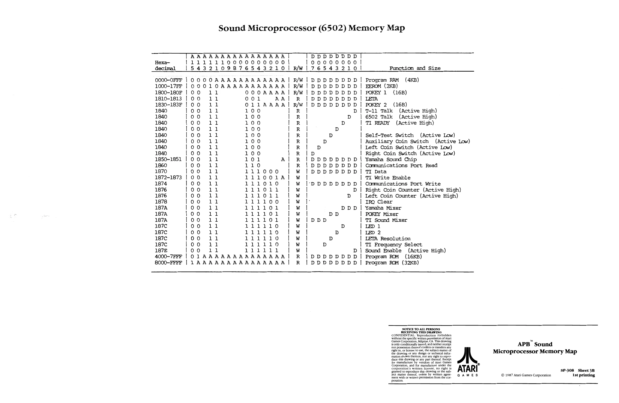
This page is a drawing, shown as the original scan.
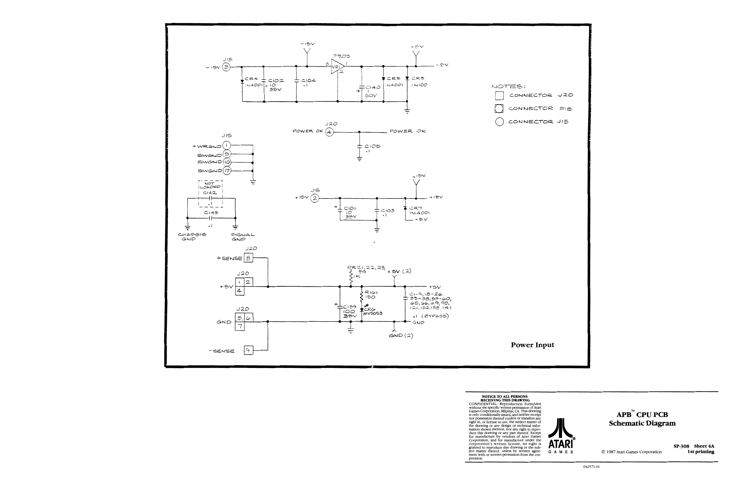
This page is a drawing, shown as the original scan.
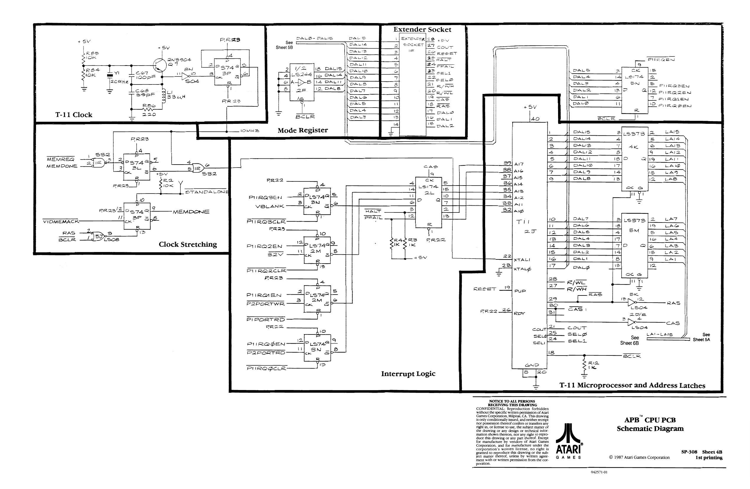
This page is a drawing, shown as the original scan.
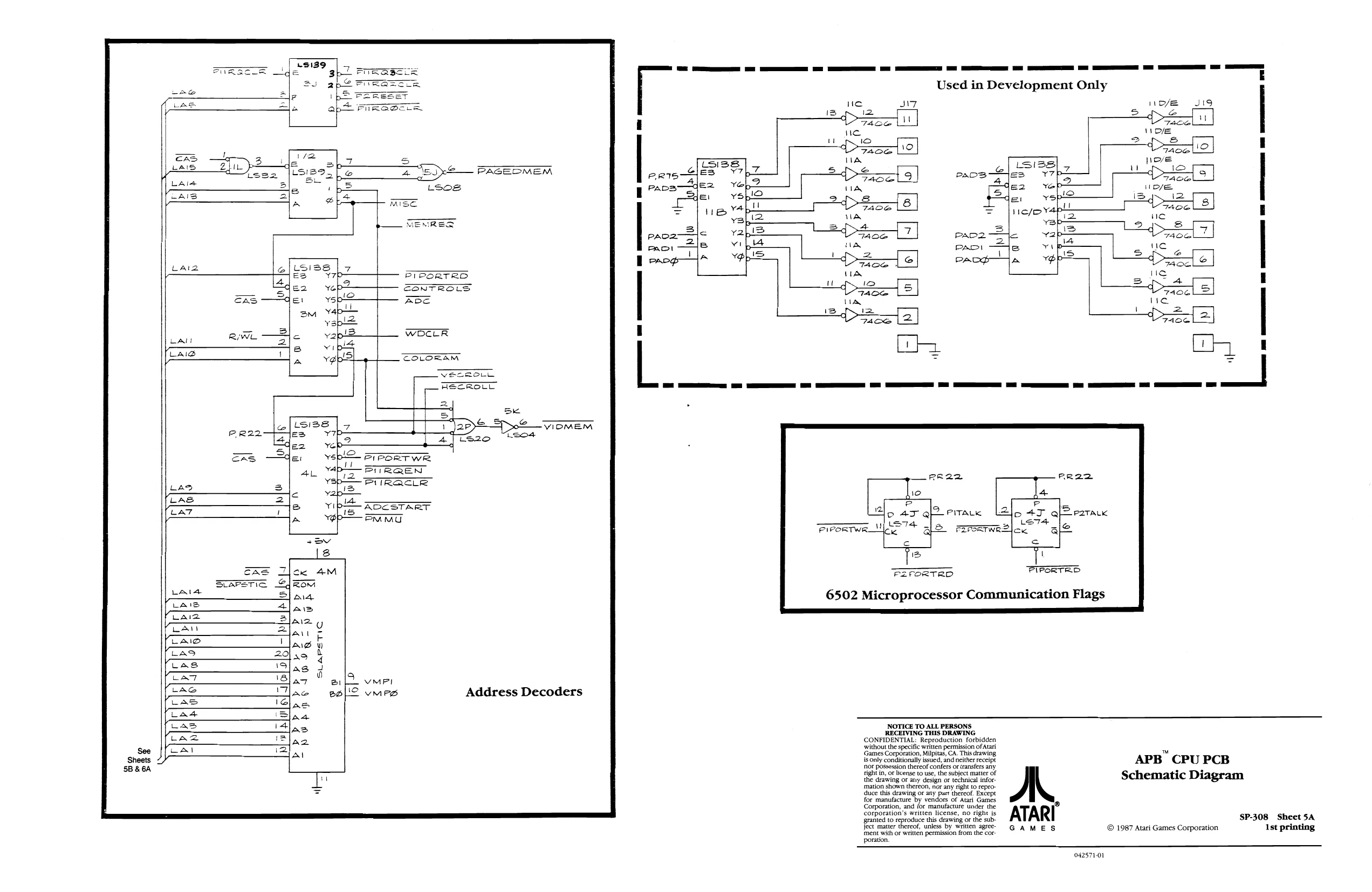
Used in Development Only
FIRaGeLe Noe S19
PAGEDMEM PADS
PAD2
PADI PACS
PIPORTRD
ESNTROLS
p— ABE oo at A A a SY re
PIPORTWR
Br RQEN PrRAcLe
2 ia Ss SO erark L2lo 47 alB rata Ls74_ oy ADESTART
ENC al® saree? a FIPORTWR,
c CS
= FIPGRTRE PZFORTRD ROR Te.
6502 Microprocessor Communication Flags
o a
a
Address Decoders
NOTICE TO ALL PERSONS RECEIVING THIS DRAWING CONFIDENTIAL: Reproduction forbidden
‘without the specific written permission of Atari
Games Corporation, Milpitas, CA. This drawing
ae Coreen, munis Ch Tae arg APB" CPU PCB Aghtinvor eens tase, the subject mater oF te ating ots dei tae nice M Schematic Diagram mation shown thereon, nor any right to reprodlce this drawing or any parr thereof Except for manufacture by vendors of Atari Games Corporation, and for manufacture under the 2
corporation's written license, no right is ATARI
granted to reproduce this drawing or the sub- SP-308 Sheet 5A
ject matter thereof, unless by written agree 7 Ata sC
Je memte theron unis by wmuenaeee 6G AME S © 1987 Atari Games Corporation 1st printing poration.
042571-01
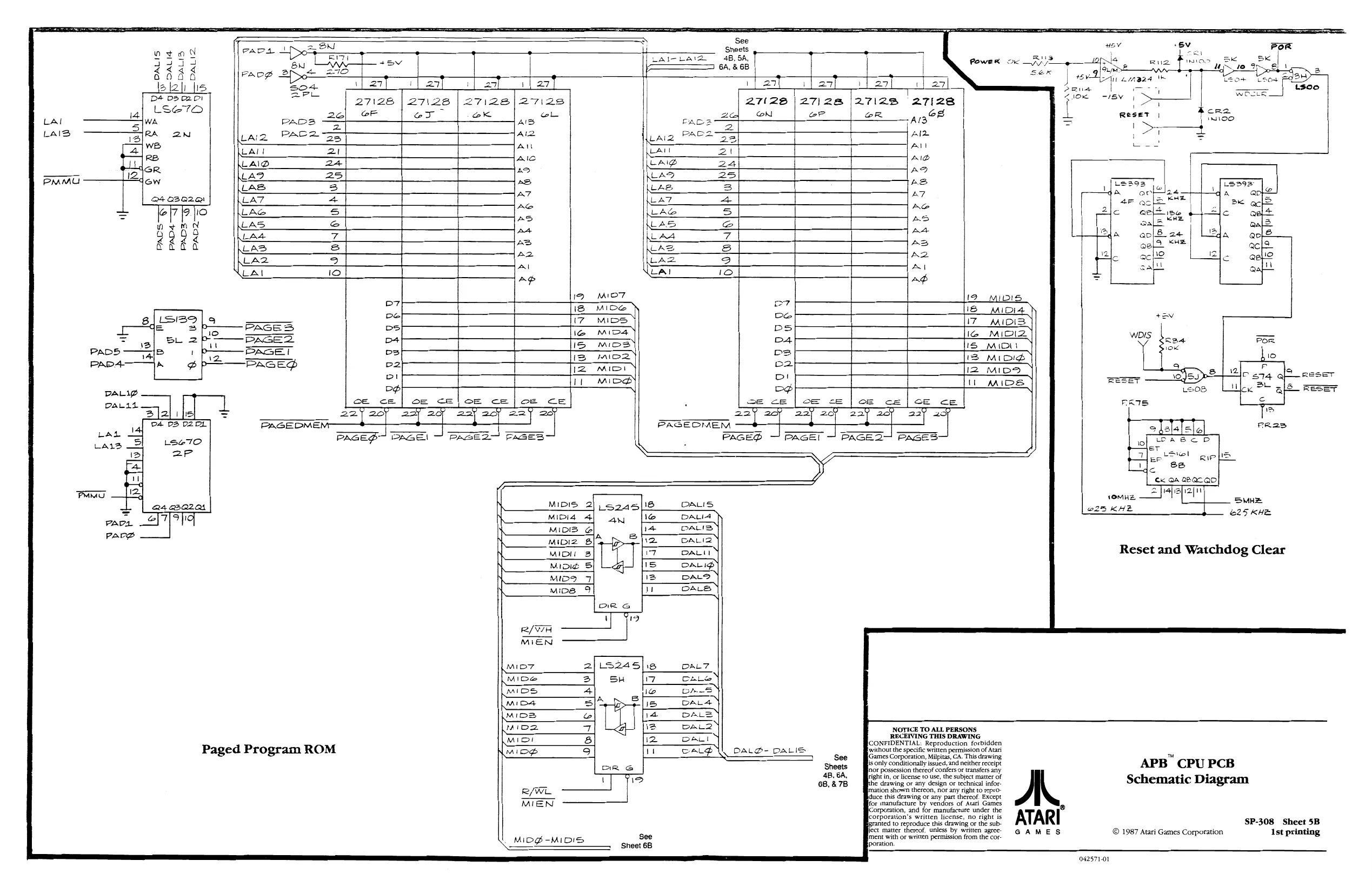
This page is a drawing, shown as the original scan.
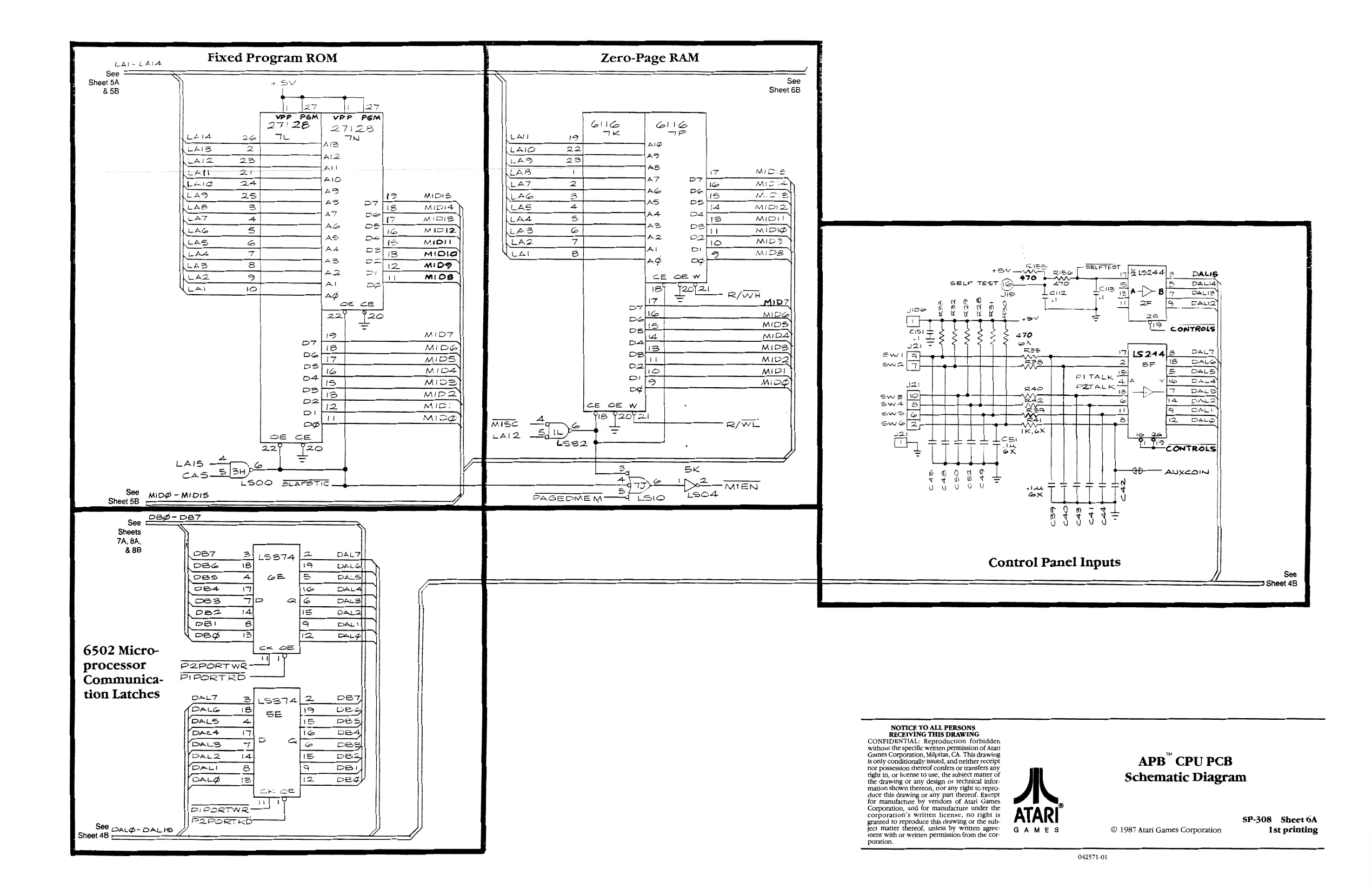
This page is a drawing, shown as the original scan.
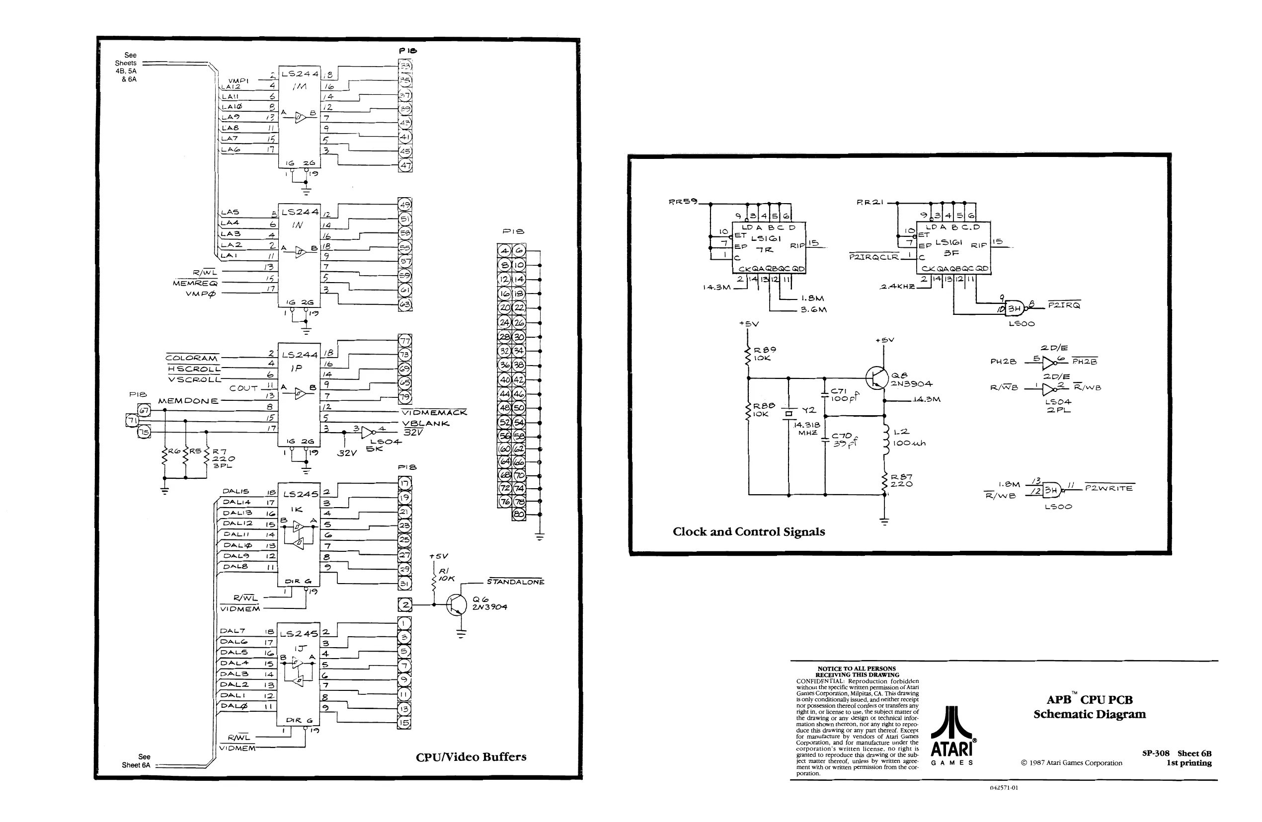
This page is a drawing, shown as the original scan.
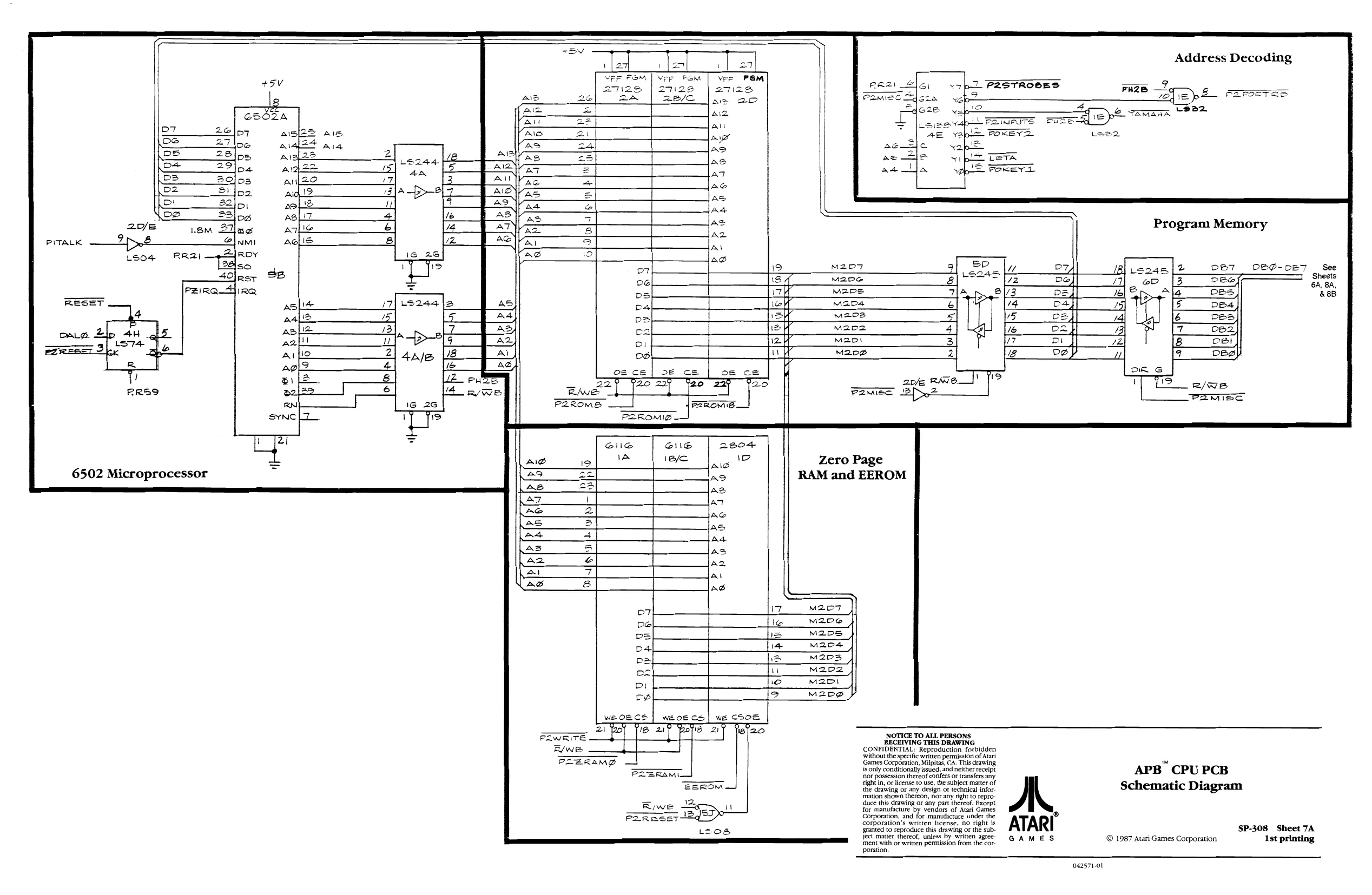
This page is a drawing, shown as the original scan.
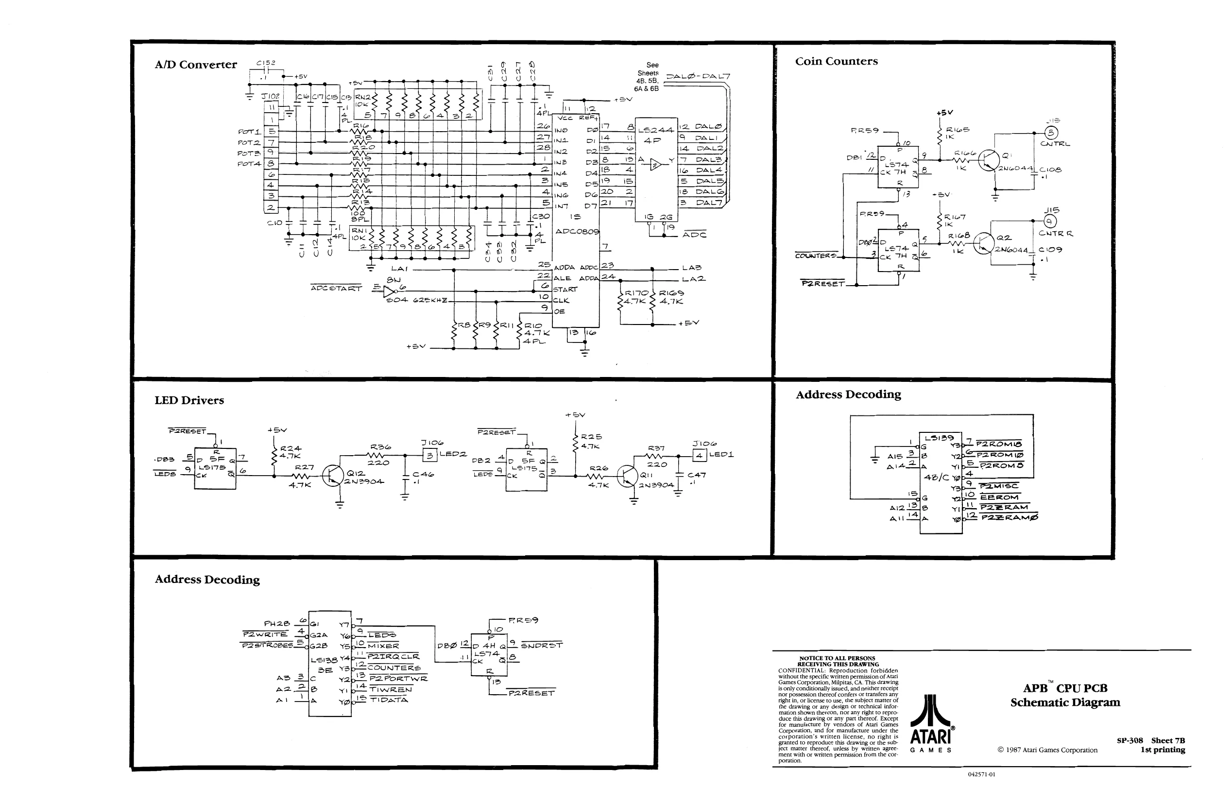
This page is a drawing, shown as the original scan.
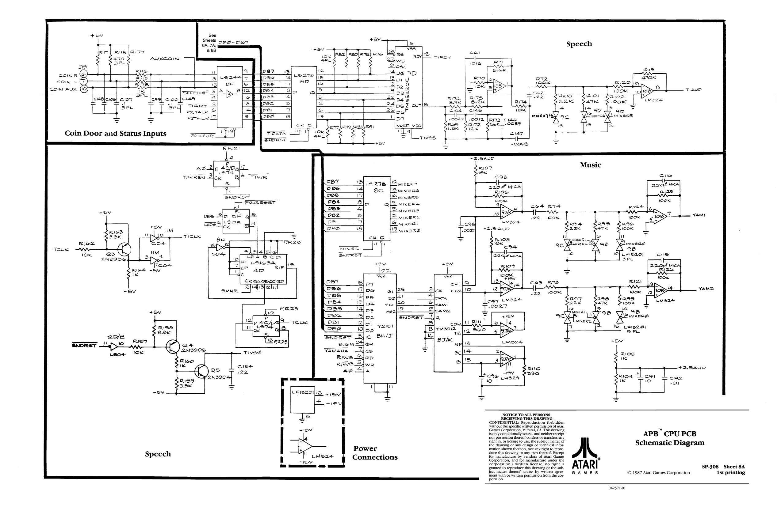
This page is a drawing, shown as the original scan.
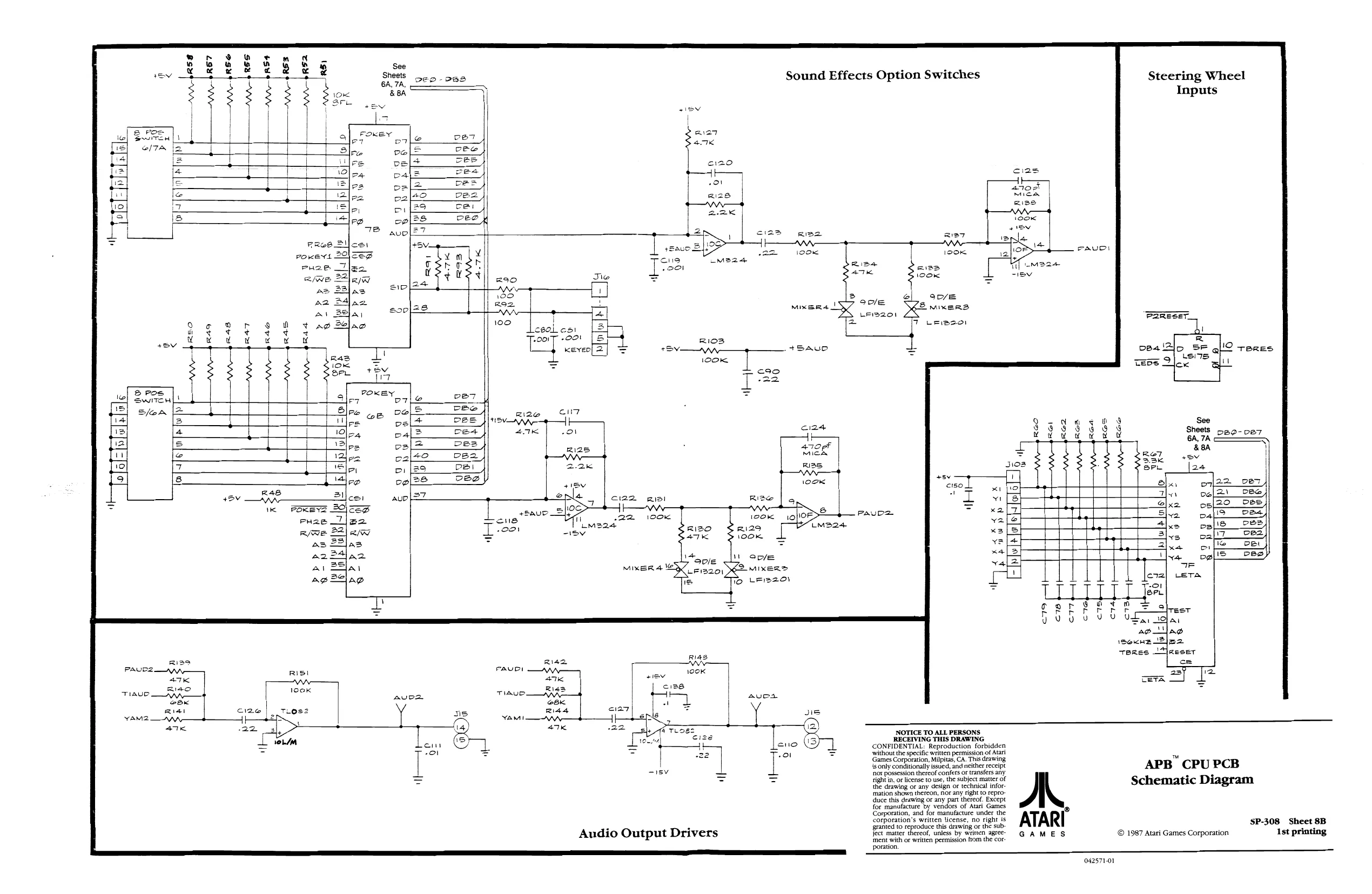
This page is a drawing, shown as the original scan.
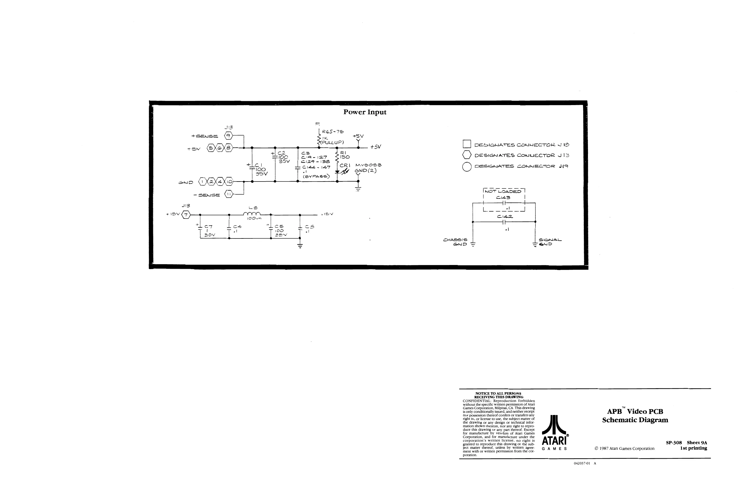
Power Input
JIB +SeUS= @) Reouls 1 +SV
PULLUP) I
+sv (8XeX8 + +5V i +2 cs RI +c! = 100 o1e-127 150 Tssv | ci29-138 CRI Mv=0s3 ff OND(2) Cad AT =FICO i mn | 3OV (BYPASS) * oO DESIGNATES CONNECTOR VID oO DESIGNATES CouuecToR J13 O DESIGNATES CONNECTOR IF
' cus
NOTICE TO ALL PERSONS RECEIVING THIS DRAWING CONFIDENTIAL: Reproduction forbidden
‘without the specific written permission of Atari
Games Corporation, Milpitas, CA. This drawing,
isonly conditionally issued, and neither receipt
‘ur possession thereof coniers or transfersany duce this drawing or any part thereof. Except
right in, or license to use, the subject matter of the drawing or any design or technical infor ‘mation shown thereon, nor any right to repro-
for manufacture by vendors of Atari Games Corporation, and for manufacture under the corporation's written license, no right is granted to reproduce this drawing or the subject matter thereof, unless by written agree. ‘ment with or written permission from the corporation, A.
ATARI
GAMES
04203701 © 1987 Atari Games Corporation
A APB’ Video PCB Schematic Diagram
SP-308 Sheet 9A Ist printing
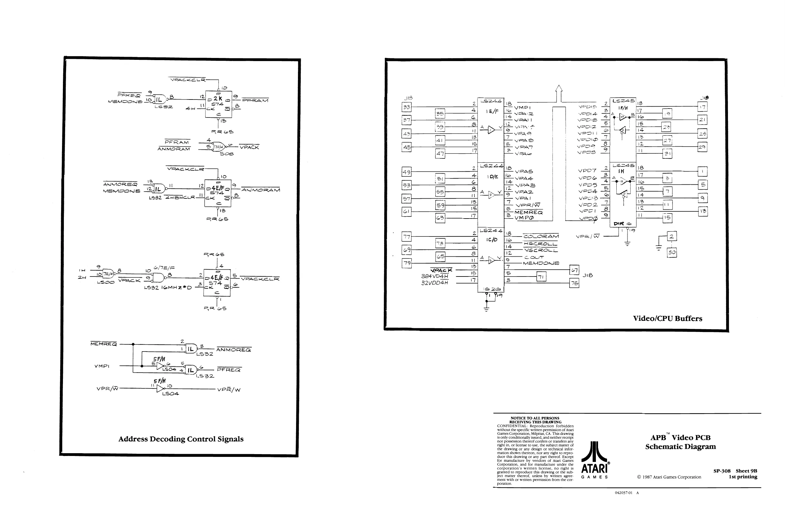
This page is a drawing, shown as the original scan.
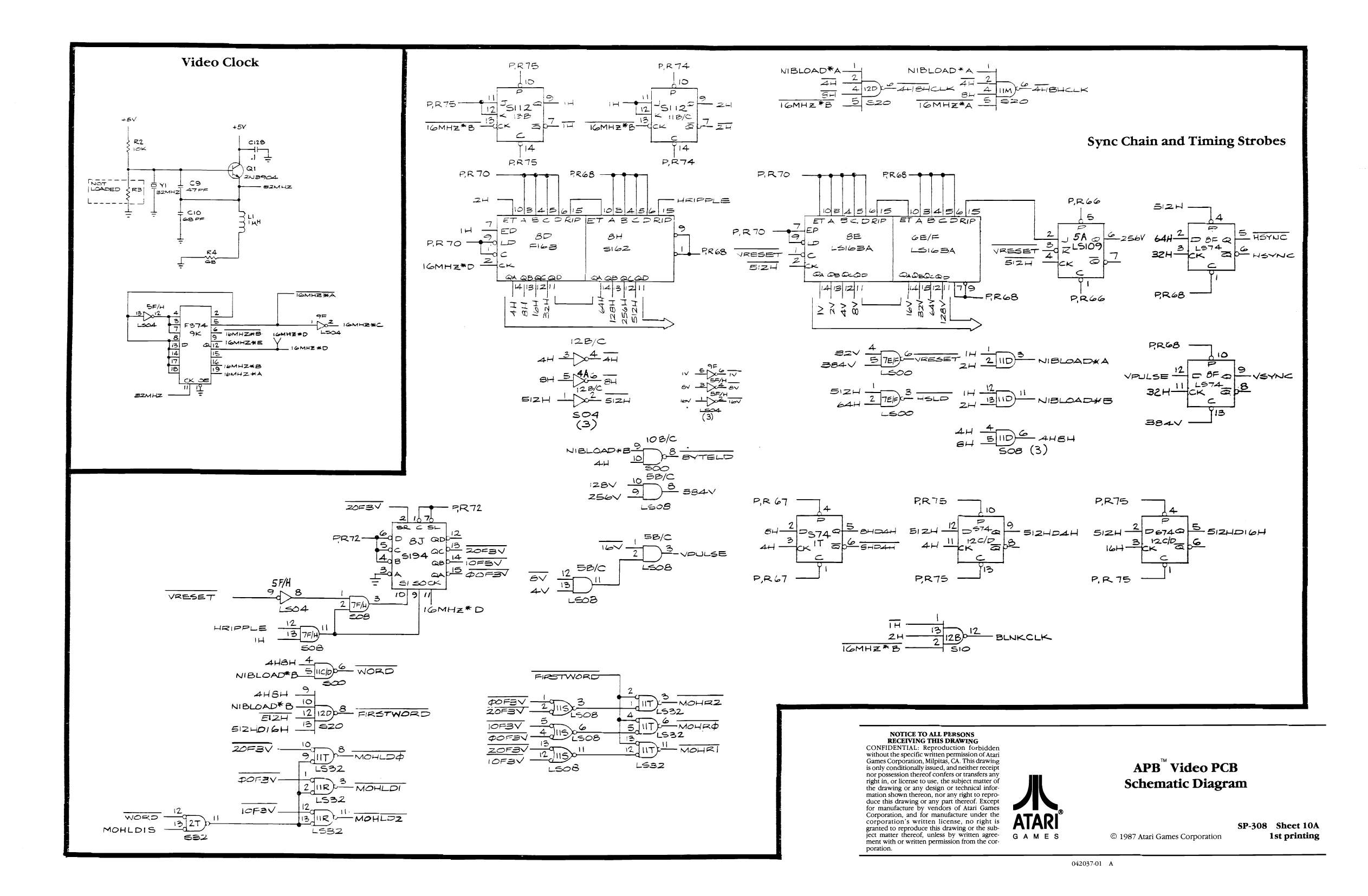
This page is a drawing, shown as the original scan.
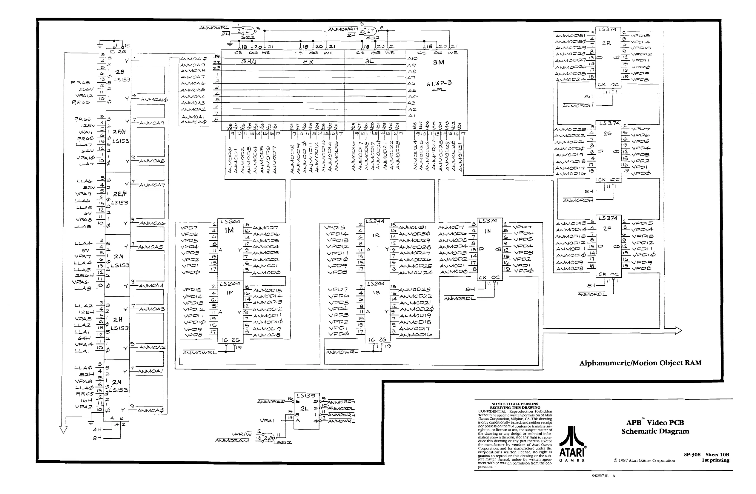
This page is a drawing, shown as the original scan.
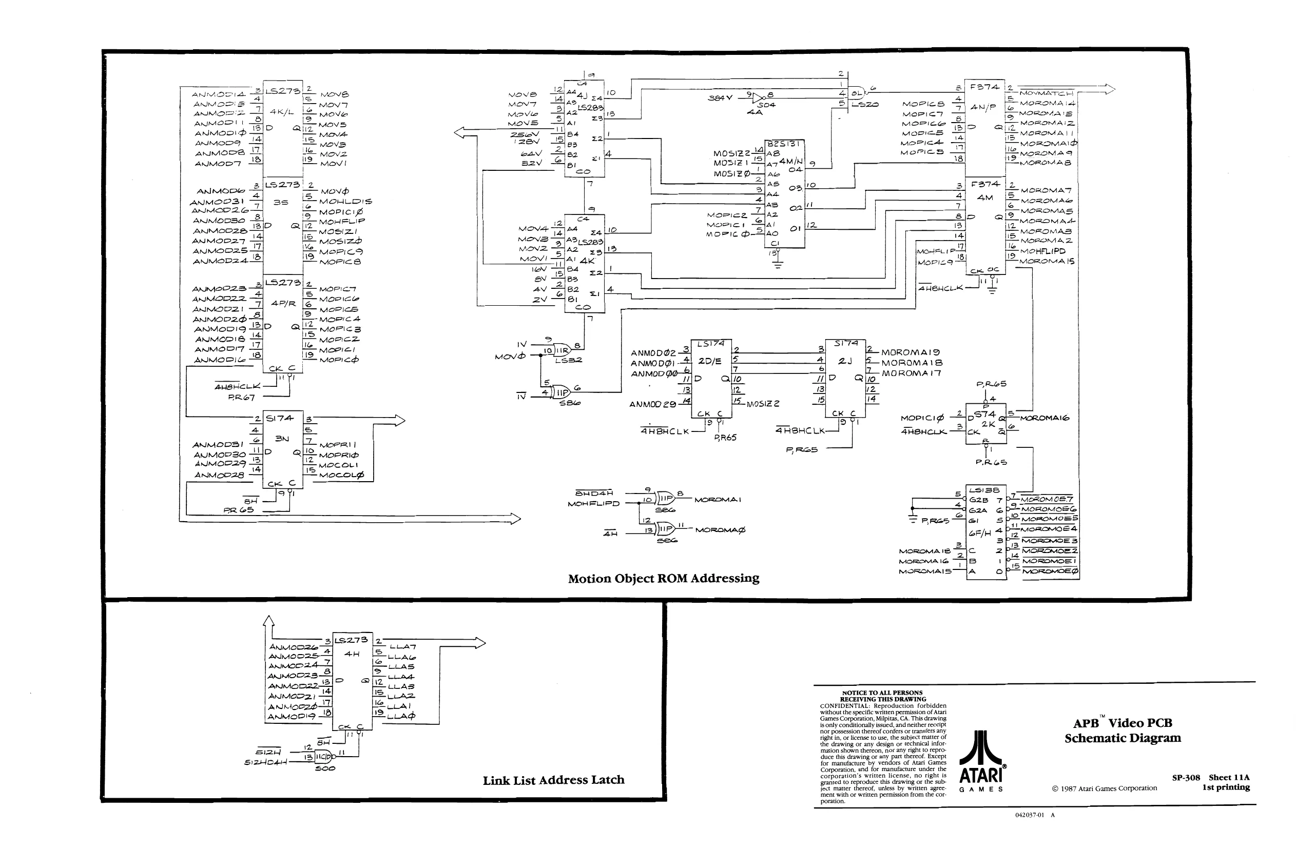
This page is a drawing, shown as the original scan.
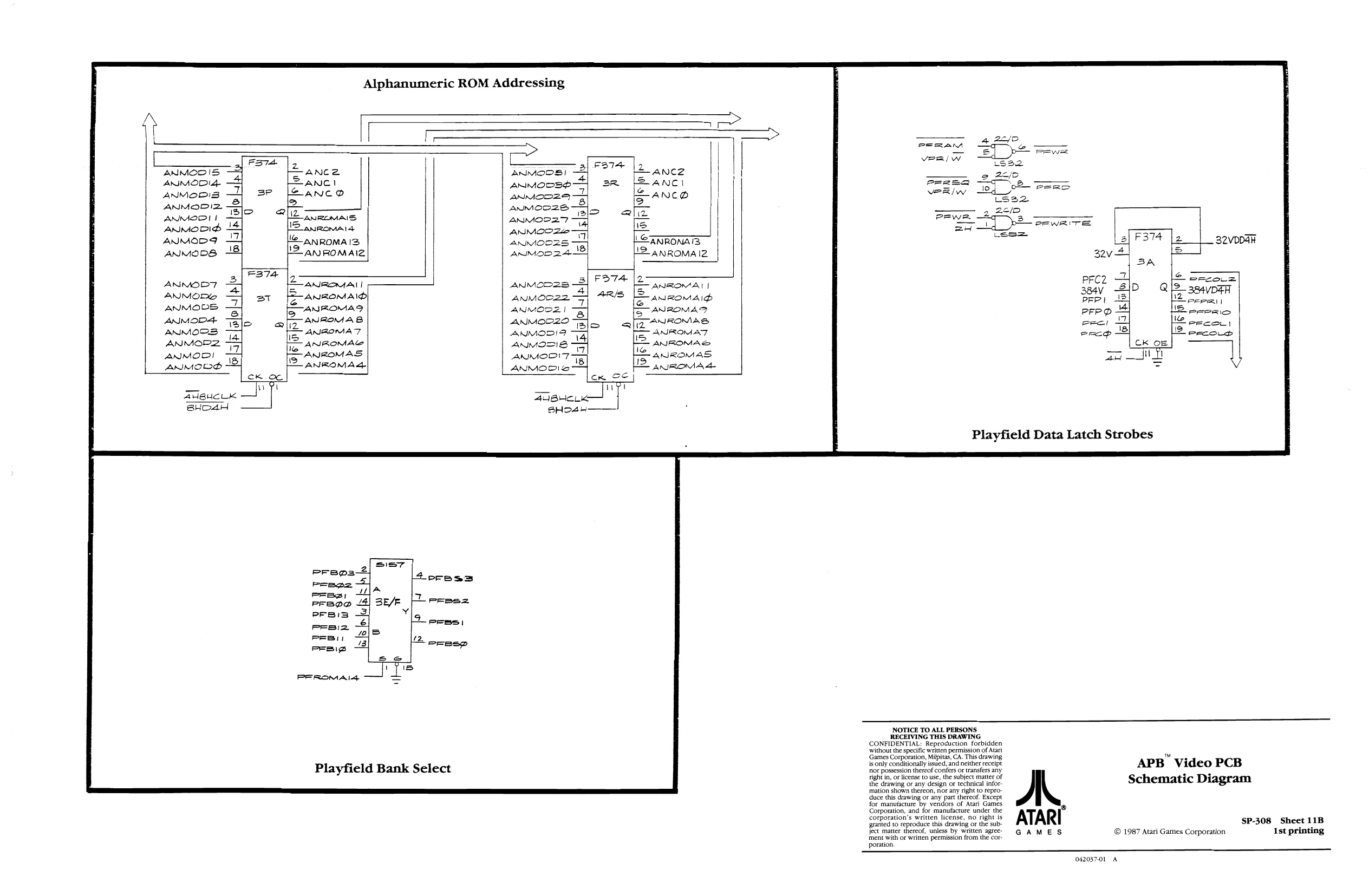
This page is a drawing, shown as the original scan.
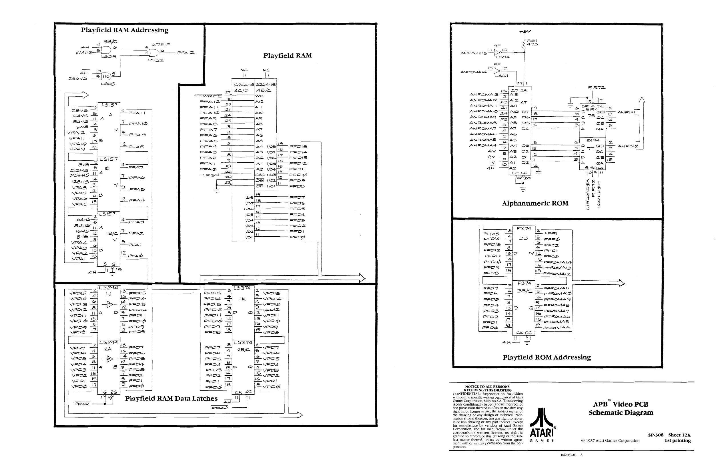
This page is a drawing, shown as the original scan.
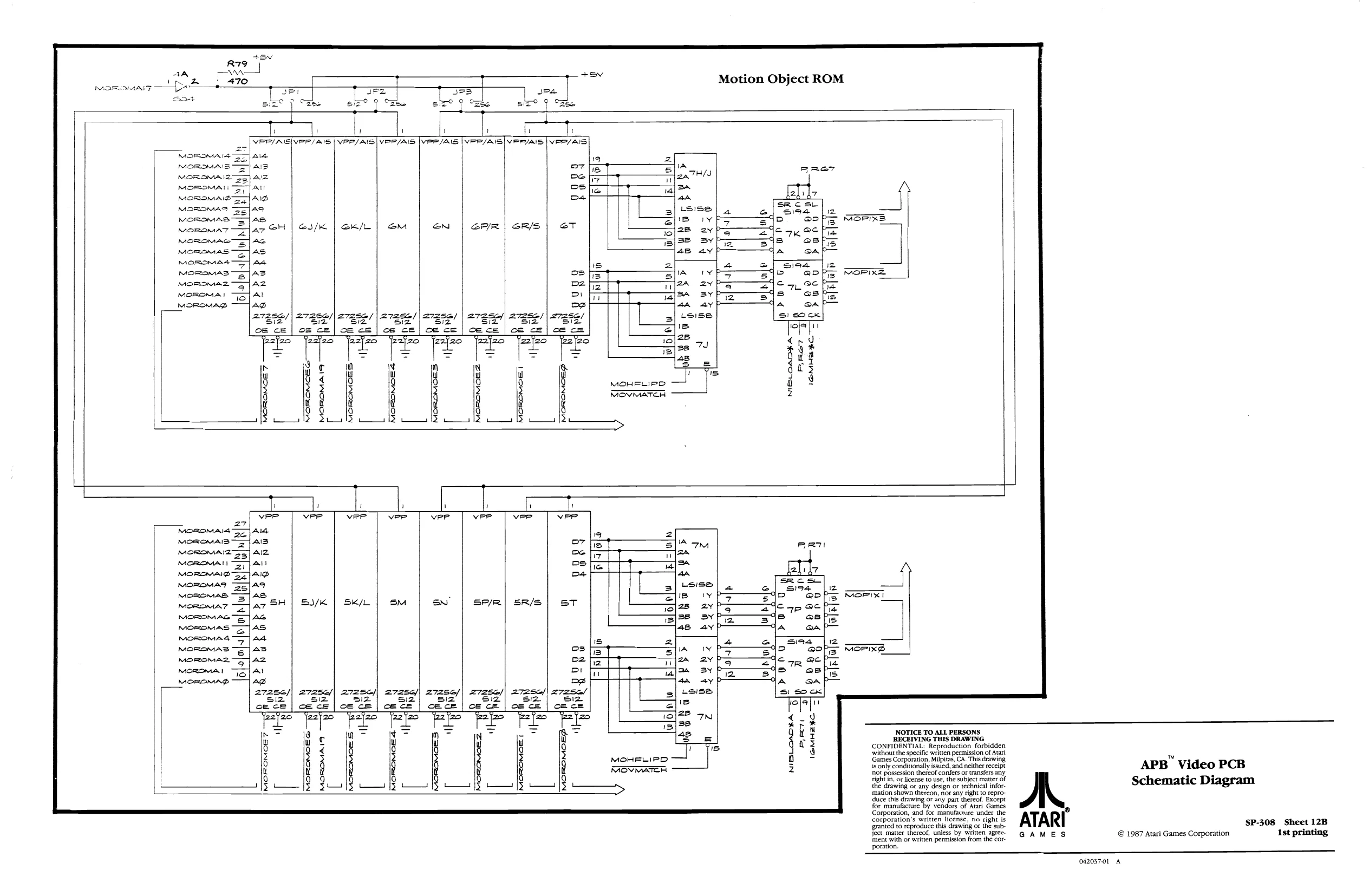
This page is a drawing, shown as the original scan.
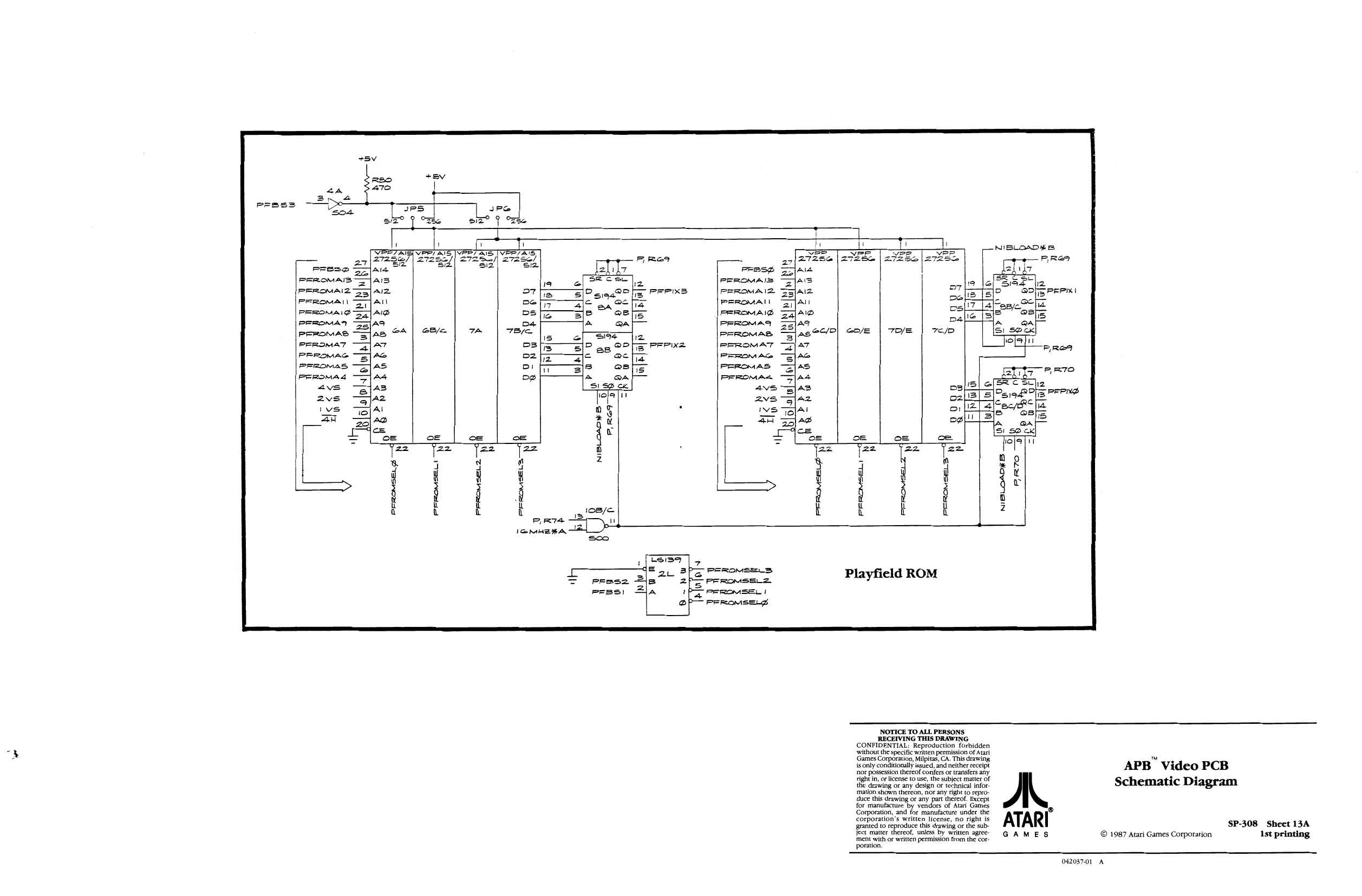
This page is a drawing, shown as the original scan.
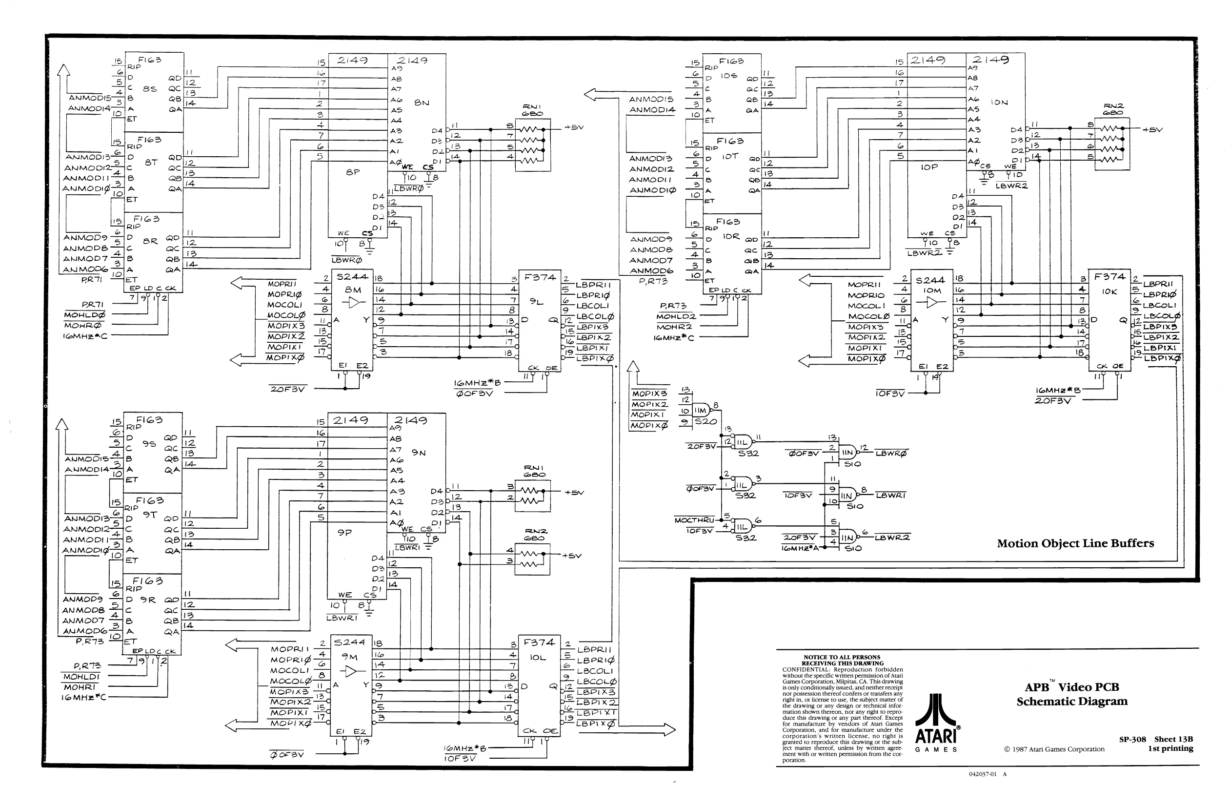
This page is a drawing, shown as the original scan.
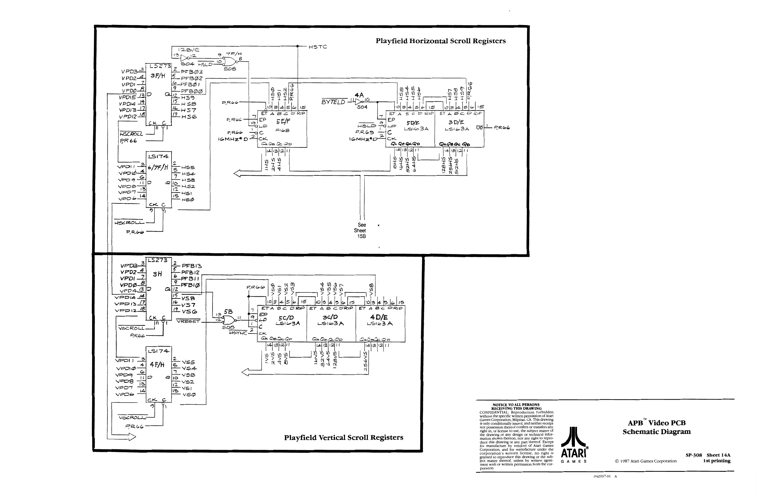
This page is a drawing, shown as the original scan.
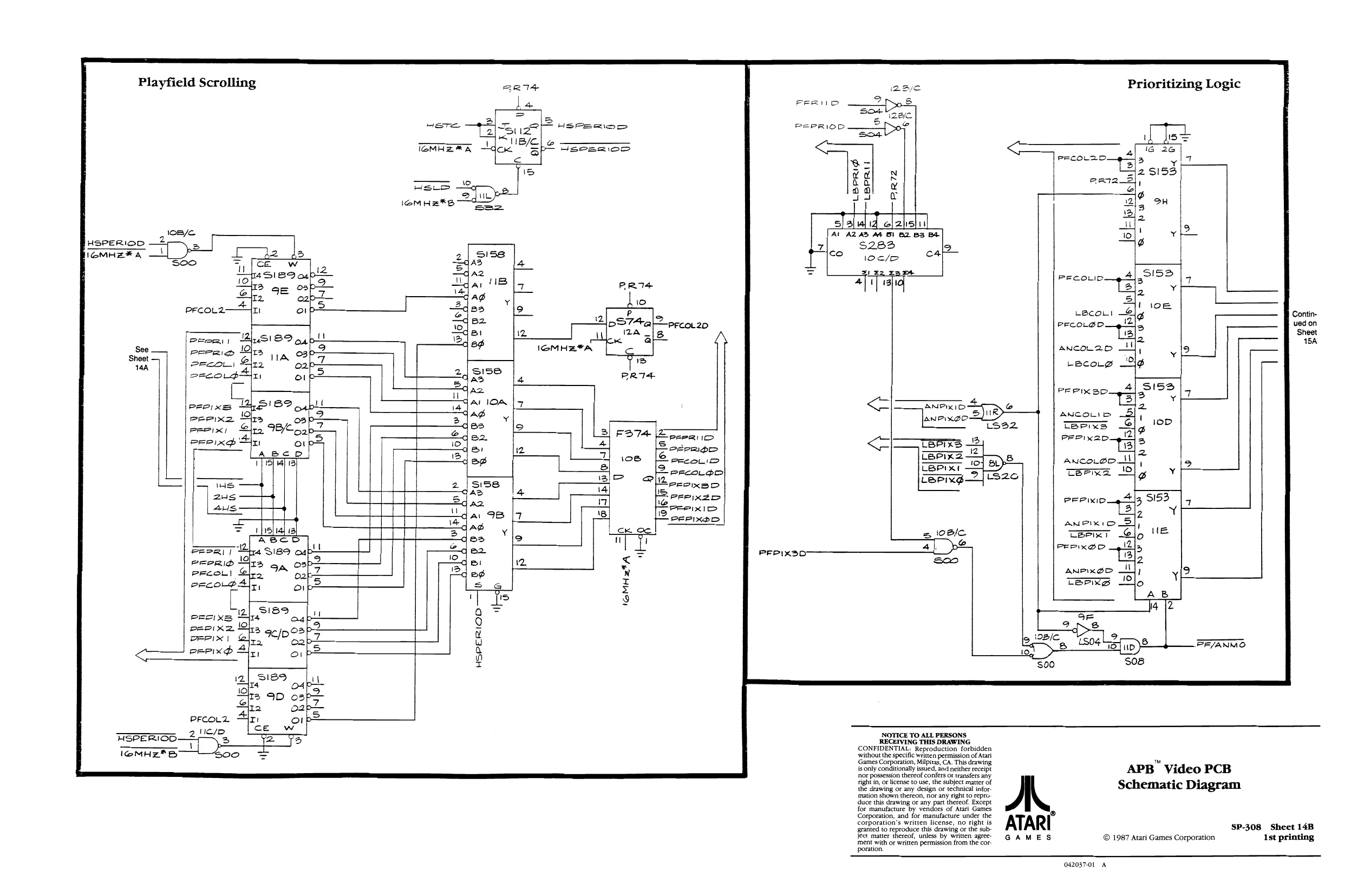
This page is a drawing, shown as the original scan.
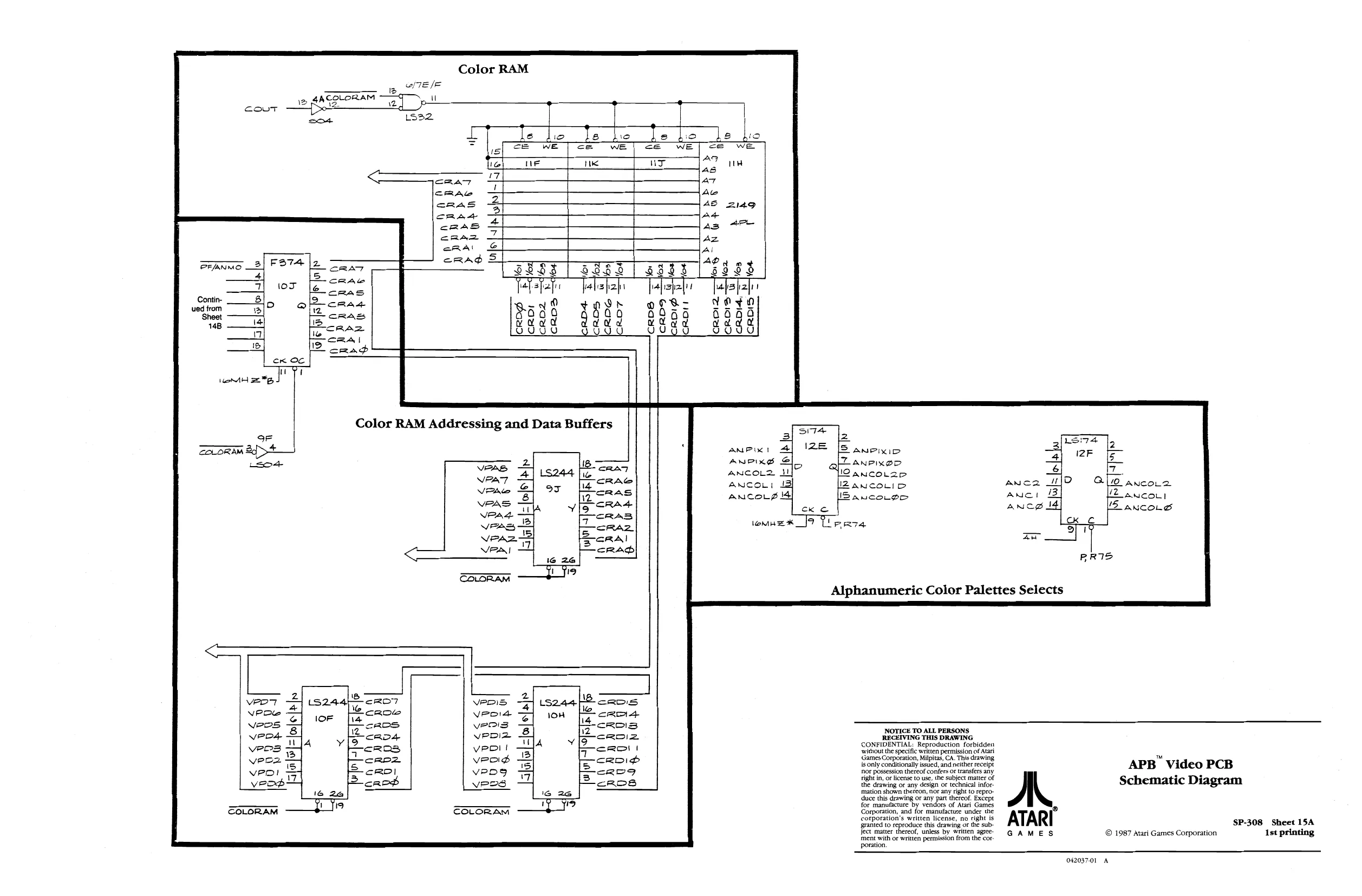
This page is a drawing, shown as the original scan.
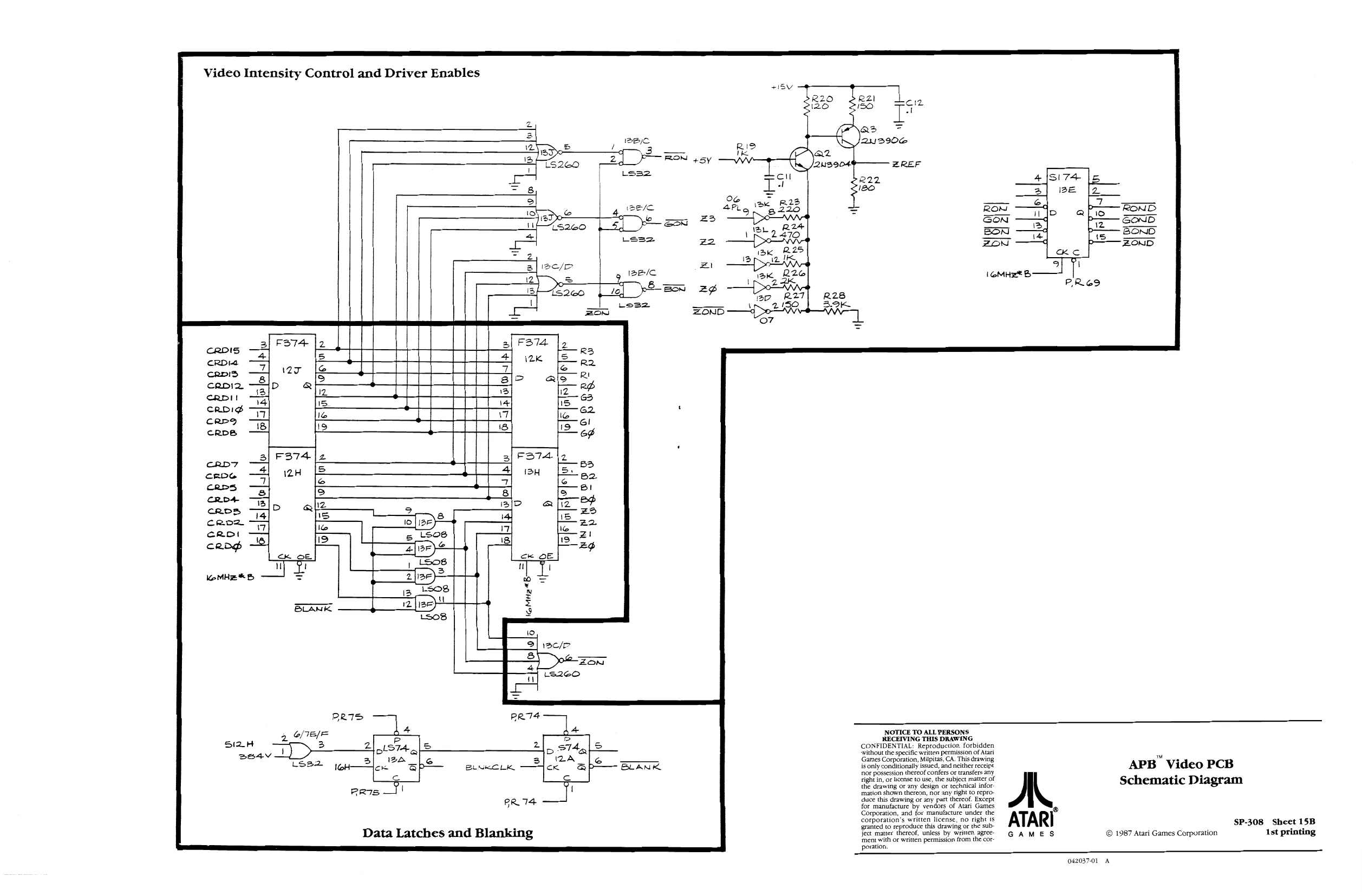
This page is a drawing, shown as the original scan.
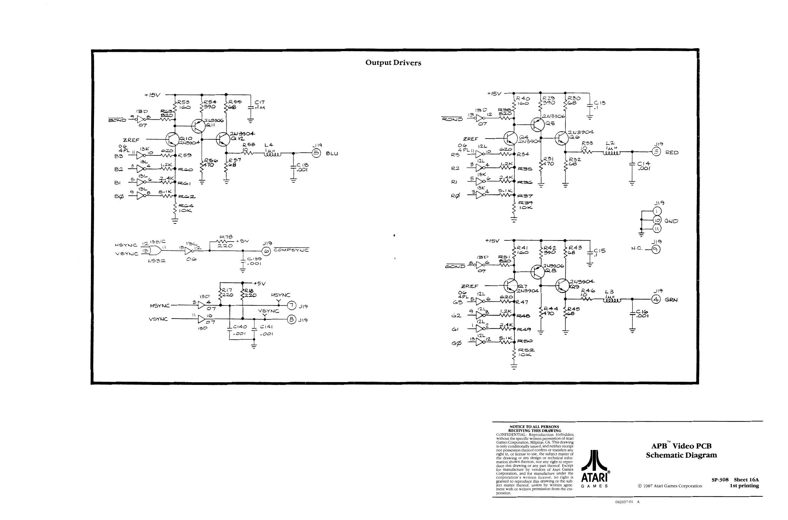
This page is a drawing, shown as the original scan.