Missile Command Caberat DP-158-1st-02A
Missile Command (rev 3, A035467-02/04 PCBs) (Atari, 1980) · Drawing Package · 1 pages · original scan
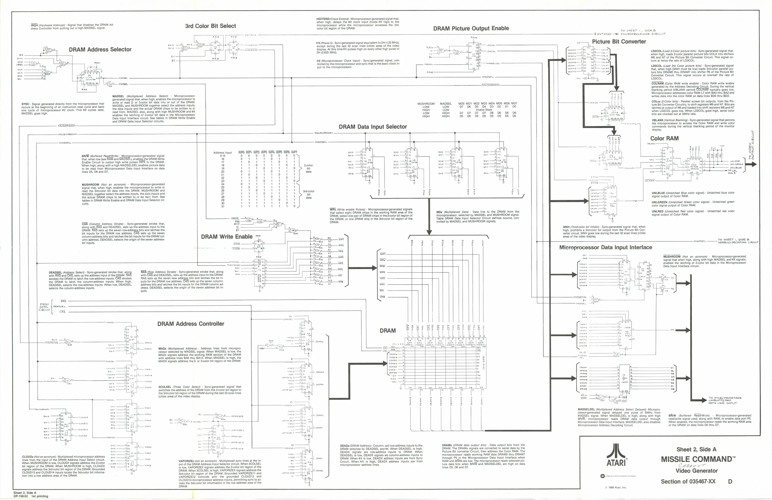
‘GEXTEND (Clock Extond)- Microprocessor generate signal tha,
wen high, delay the 60 clock Input (nolas @0 higy) to the
Imicroprocessor while the microprocessor accesses the 3rd olor Bit region of the DRAM, ROR (Haraware Interrupt) - Signal that disables the DRAM A tees Controlier from putting outa high MADSEL signal 3rd Color Bit Select DRAM Picture Output Enable To SKEET 1, SIOES BEXTEND = MicROPRoCe'sso® CIRCUIT ent to 2H (125 MH, fexcept duting tho last 32 scan lines (iis area) ofthe video rome ‘play, At tne time 9X pulses high on every other high pulse of 2a (odes Me. Picture Bit Converter DRAM Address Selector
0 (Microprocessor Clock input Sync-generated signal, con: es trolled by the microprocessor and sync thats the basi clock in- aan put to the microprocessor. ce L020 (Loa 2Coter picture bts)- Syne-gonerated signal tat, when high, loads 2color parallel picture bits COLX into shifter IMB and N7 of tho Picture Bit Converter Cicult. This signal c- ‘urs at twice the rate of LOSCOL. LD2COL (Losa ard Color picture bits) - Syne generated signal that, when high GINH must be low) loads srcoler paral pie {ure bits DRAMO thru DRAM? into shifter PS ofthe Picture Bit Converter Gicult. This signal occurs at onehalf the rate of toacot
SYNC - Signal generated directy from the microprocessor that ‘occurs atthe Beginning ofan instruction read cycle and lasts fone_cyelo of microprocessor @2 clock. Five 00 cycles later, MADSEL (Multiplexed Address Select) - Microprocessor: {Generated signal that, when high, enables the microprocessor to Write of read 2- or color Bit data into or out of the ORAM. MABSEL and MUSHROOM together select the address input, the data Inputs and the actual DRAM chips toe writen to oF MUSHROOM Low MADSEL MOO MDI MD2 MDs MD4 MDS
| tow | "D706 | DS | D403 | D2 |
tow Iavalid State ‘TOLRAM (Color RAM write enable) - Color RAM write enable ‘generated bythe Address Decoding Circuit During the vertical Banting pevog (VSLANK period) COLRAWE typicaly goes low
Microprocessor addresses color RAM L7 with BAO thru BA@ and
writes data Into the color RAM on data ines BDO thru BOS. ‘COL (2Color bits) Paalolsereen bit outputs, from the Pic ture Bit Converter Circuitry, to shift registers MB and NT. Bits are latened at output of NE and loaded into shift resistors MB ana N7
ead from. MADSEL also along wih high MUSHROOM and @X HIGH
| fenables the latching of color bit data In the Micro | Low | HIGH | 07 | 07 | D7. | D7 | 06 | 06 |
| Data Input Interface circu. See tables In ORAM Write Enable | HIGH | HIGH | D505 | 055 | DS | DS. |
fand DRAM Data input Selector circuits.
MADSEL goes nigh ‘when LDZCOL goos low. When LD2COL goes high, sell color
Dis are clocked out at SMHP rate. BLANK (Vertice Blanking) - Syne generated signal that permits the mleroprocassor to aczess tho Color RAM and write color ‘Commands Curing the vertical Blanking period of the monitor ‘display
Color RAM DRAM Data Input Selector
t sans
‘Ass Input BRAW (Butfored ReadiWrite) - Microprocessor generated signal ‘O18 ‘that, when low (see PAW and “enables the DRAM Write 6 Enable Crcut to output high write pulses WPX to the ORAM. 7 ‘When high, along with a high MADSELDEL enabies picture data| 8 to be read from Microprocessor Data Input Interface on data 9 lines 05, D6 and 07 Fa a
FA
MUSHROOM (Not an acronym) - Microprocessor generated 28
‘signal tha, when high, onables the microprocessor to write oF Fa {oad the Sid-color bit data into the DRAM. MUSHROOM and Fs [MADSEL together select the address inputs, the data inputs and Z the actual DRAM chips to be writen fo or be revs from. See 23 tabea in DRAM Wille Enable and DRAM Data Input Selector ct 2 cults. Fy EY To viogo Ourbur ciecur
Pos? ge
a) LUNLBLUE (Uniatched Blue color signa) - Unlatched blue color signal output of Color RAM,
UNLGREEN (Uniatched Green color signal - Unlatched green
Color signal output of Color RAM. oe | sas srorssonssos-0¥ aesrorstonssonnno¥ SO receee | aaiousas-asettuossd totes nsross sos +0¥ ehatenatersnonsae§ WE (write enable Pulses)» Microprocessorgenerated signals that select eight ORAM chips in the worklrg FAM area of the DRAM, select one pair of DRAM chips in thezcoor bit region of ‘the DRAM, or one DRAM chip in the Se-coor bit region of the MDx (Multiplexed Data) - Data tine to the DRAM trom the Imleroprocessor, selected by MADSEL and MUSHROOM signa. ‘Table DRAM Data Input Selector Circuit detines source, con UNLRED (Uniatched Red color signal) - Unlatched red color signal output of Color RAM. ERS (Column Address Strobe) - Sync generated strobe that, DRAW. {tolled by MADSEL and MUSHROOM signals. slong with FAS and DEADSEL, sets up the address input to the (DRAM: RAS sets up the soven row-adaress bits and latches the Dit inputs for the DRAM row adgress. GAS sets up the seven Colurmnadress bts and atches the bit inputs fr the DRAM col tr adress. DEADSEL sales he org of te seven adres. itinputs. SINH (Thickcolor bit inhibi - Syne generated signal that, when igh, prohibits a Sr.colr bit output trom the Picture Bit Con ‘eter crcult SINK goes ow during the last 32 scan lines (ities ‘area of the video display ro SHEET 1, SIE —— ‘ApoRE SS OECODINeiReWIT aa — $e! Microprocessor Data Input Interface MUSHROON (wor an acronym) - Microprocessor generated ‘signal that when high, along with high MADSEL andeX signals, ‘enables the latching of 2e0!or bit data In the Microprocessor Data input interface circuit DEADSEL /Aduess Selec) - Sync generated strobe that, along RRS (Row Adress Sob) - Synegenentd sob tat, along with BAS and GAS seta up ine eccressnput of tne DRAM RAZ with GAB and DEADSEL, sts up th aes input fo the ORAM. robes the DRAM to latch the rowaddress inputs. CAS strobes the DRAM to latch the colummadaress Inputs. When ‘igh, DEADSEL selects the rowsddrese inputs. When low, DEADSEL, Selects the columnaddross Inputs. RAS sets Up the seven new address bits and latches the bit in: puts forthe DRAM row addross. CAS sots up the seven column [Bdaress bits ac latches the bit inputs for the DRAM eolumm ac ‘ress. DEADSEL selects the origin ofthe seven address bitin puts.
From SIRE J cxnosen cinco |
DRAM Address Controller DRAM a MADx (Multiplexed Adress) - Address lines trom micropro- Ceasor selected by MADSEL signal. When MADSEL Is low, MADx signals address the working RAM section of the DRAM with adctess lines BAO thu BAYS. When MADSEL i high, the MADX signals address tho 2. of Scolor bit region of the DRAM. Fae
SCOLSEL (Three Color Select) - Synegenerated signal that ‘witches the address ofthe DRAM from the 2-color Bt Fogion to ‘the dolor Bt region ofthe ORAM during the ast 32 sean lines (eis area} of the video display. Temicecreocessoe DATA LIDE INPUT
MADSELDEL Multiplexed Address Select Delayed) Micropro- Ccessorgenerated signal delayed one pulse of SMH from MADSEL signal. When MADSELDEL is high, along with high SBA woes BRW (Buttered AaadiWrite) - Microprocessor-generates microprocessor reads DRAM data" output’ through readiwrite signal used, along with RAM, to enable dataport PS. Microprocessor Data Input Interface, MADSELDEL algo disables When enebieg, the microprocessor reads the working RAM area Microprocessor Acdrese Decoding Circuit fof the ORAM on data lis 00 th DT.
eas. P a DEADx (ORAM Address) Column ad row-address inputs tothe DRAMx (ORAM data output its) - Data output bits from the ‘CLOUDx Not an acronym): Multiplexed microprocessor address lines trom the input of the DRAM Address Input Select circuit ‘when MUSHROOM is low, CLOUDX signals address the 2.color Dit gion of the ORAM. When MUSHROOM s high, CLOUDX Signals address the 3récolr bit rgion of the DRAM. Grounded CLOUDIS and CLOUDY Inputs locate the Se-color Bt Informa: tion into a low address area of the DRAM.
Sheet 2, Side A DP-158-62 1st printing soe \VAPORIZEx (not an acronym). Multiplexed syne lines at the inputof the ORAM Address Input Selector circut. When SCOLSEL [blow VAPORIZEX signals address the 2coor bit region of the ‘DRAM, When 3COLSEL Is high, VAPORIZEX signals address the Sracolor Bt vogion of ihe ORAM. Grounded VAPORIZETT and \VAPORIZE12 coincide "with the grounded CLOUDIS and CLOUD microprocessor address inputs, permiting syne toa ‘Sess the Stdcolor bit information in the iow address aea of the ORAM. DRAM selected by DEADSEL and. When DEADSEL is high, DEADX signals. are. row.addross inpute. to. ORAM. Whoa DEADSEL Is low, DEADX signals are columm-address inputs to DRAM. When @x Is low, DEADX adiress Inputs are trom Syne ‘Circuit. When @X is high, DEADX address inputs are from microprocessor adsress lines. ‘ORAM. The ORAM signals are converted to serial data by the Picture Bit converter Circuit, then address the Color RAM. The ‘microprocessor reads working FAM data DRAMO thru ORAM? through P5,in the Microprocessor Data Input Inertaco when RAM and BAW are low. The microprocessor reads selected pie ture data bits when BAUW and MADSELDEL are high on data lines 05,06 and 07. A ATARI Sheet 2, Side A MISSILE COMMAND™ Cubs eT Video Generator
Section of 035467-XX D