Dig Dug SP-203 1st Printing
Dig Dug (rev 2) (Namco, 1982) · Schematic Package · 16 pages · 37 sections · original scan
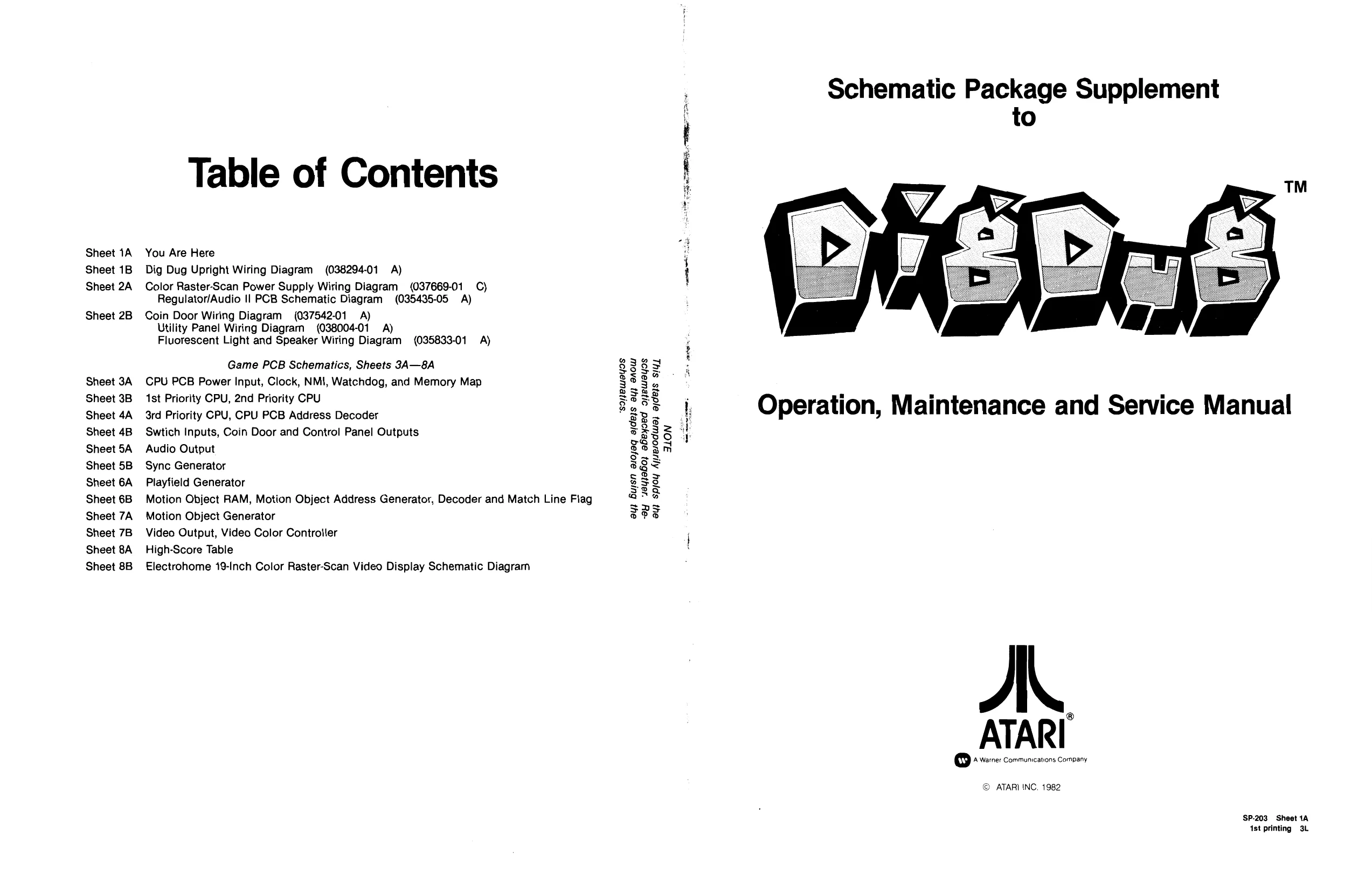
Sheet 1A Sheet 1B Sheet 2A
Sheet 2B
Sheet 3A Sheet 3B Sheet 4A Sheet 4B Sheet 5A Sheet 5B Sheet 6A Sheet 6B Sheet 7A Sheet 7B Sheet 8A Sheet 8B Table of Contents
You Are Here Dig Dug Upright Wiring Diagram (038294-01 A) Color Raster-Scan Power Supply Wiring Diagram (037669-01 C) Regulator/Audio I! PCB Schematic Diagram (035435-05 A) Coin Door Wiring Diagram (037542-01 A) Utility Panel Wiring Diagram (038004-01 A) Fluorescent Light and Speaker Wiring Diagram (035833-01 A)
Game PCB Schematics, Sheets 3A—8A CPU PCB Power Input, Clock, NMI, Watchdog, and Memory Map 1st Priority CPU, 2nd Priority CPU 3rd Priority CPU, CPU PCB Address Decoder Swtich Inputs, Coin Door and Control Panel Outputs Audio Output Sync Generator Playfield Generator Motion Object RAM, Motion Object Address Generator, Decoder and Match Line Flag Motion Object Generator Video Output, Video Color Controller High-Score Table Electrohome 19-Inch Color Raster-Scan Video Display Schematic Diagram “sonewseyos ay} Buisn a1ojaq ajdejs ay} aaow Schematic Package Supplement to
Operation, Maintenance and Service Manual -ay seayjabo} abeyoed ojjewayos ey) spjoy Ajsesoduia) ajdels siyy
JLON
A ATARI ] + Warner Communications Company
© ATARI INC. 1982
SP-203 Sheet 1A 1st printing 3.
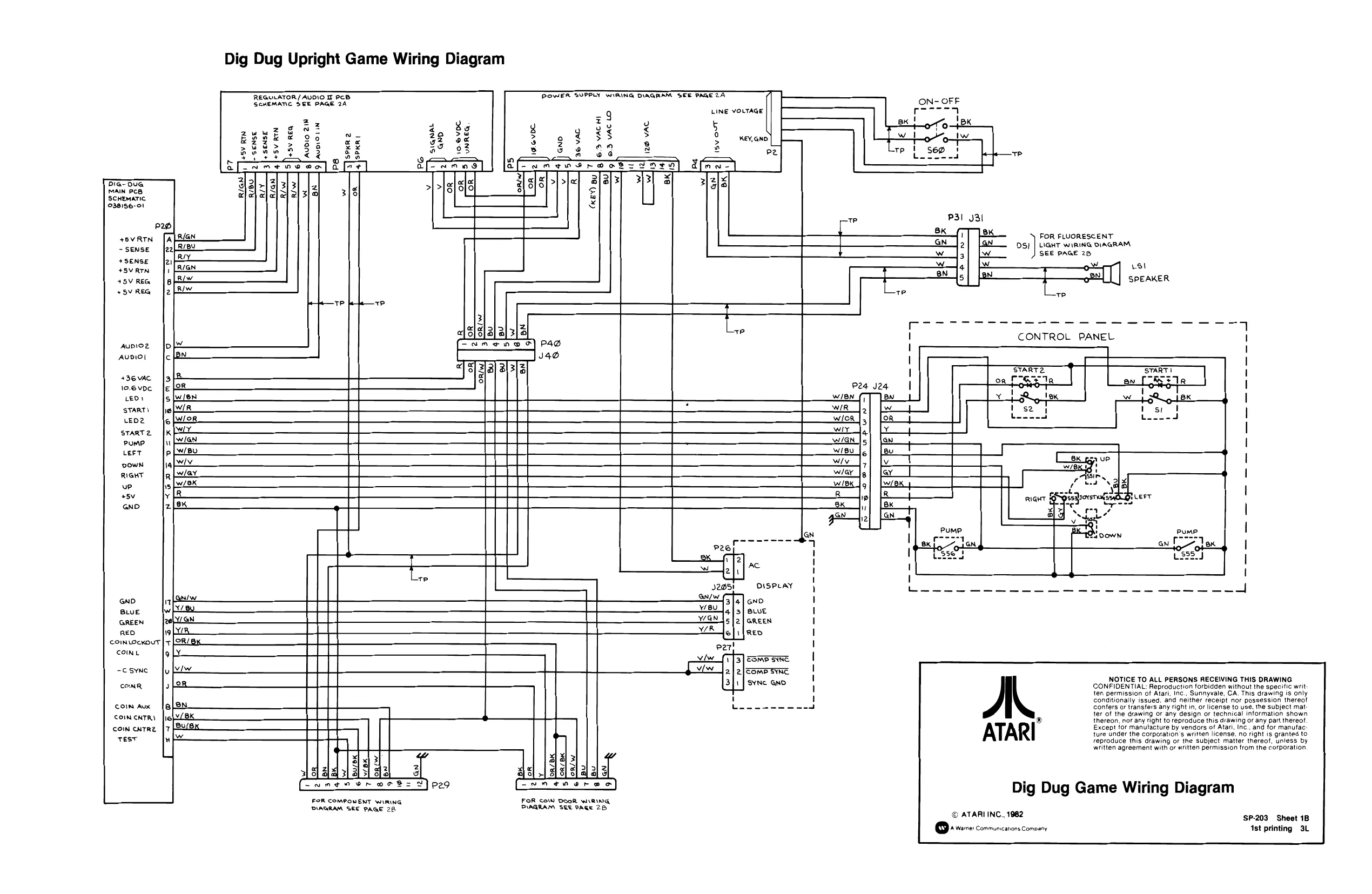
This page is a drawing, shown as the original scan.
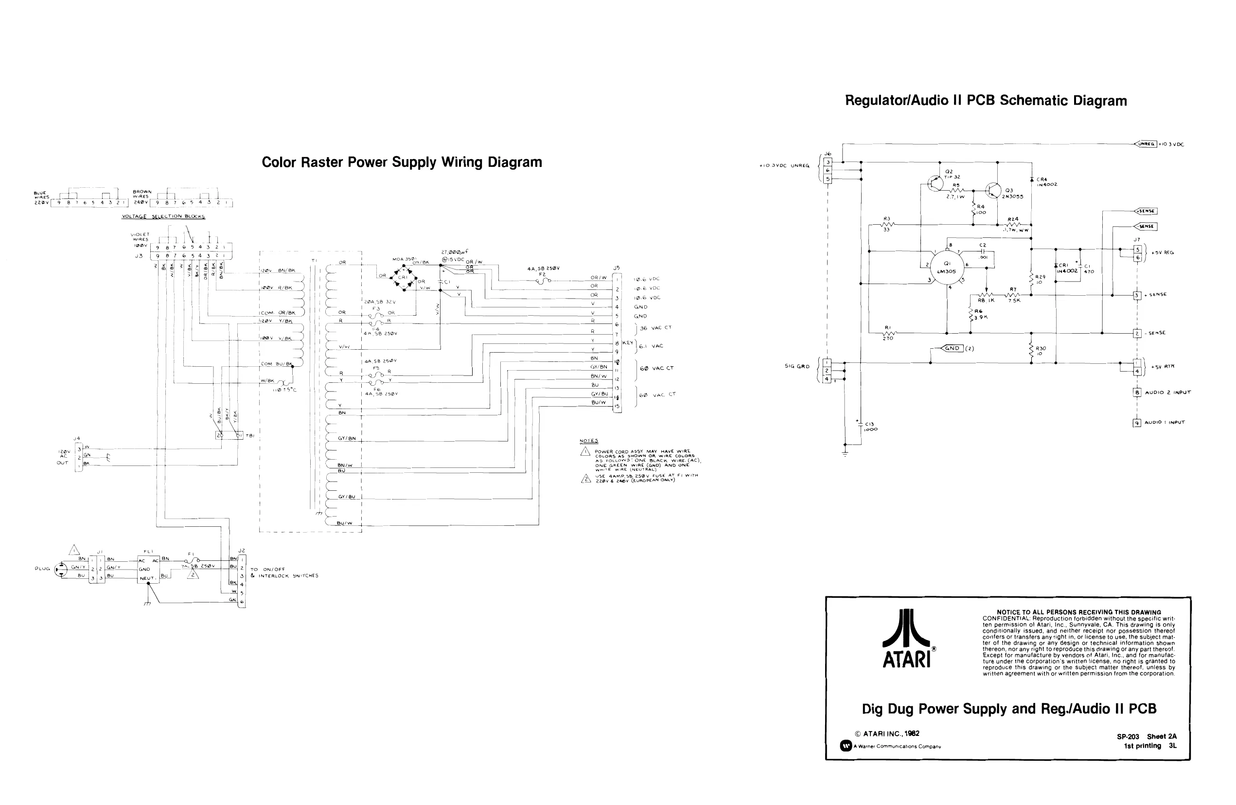
This page is a drawing, shown as the original scan.
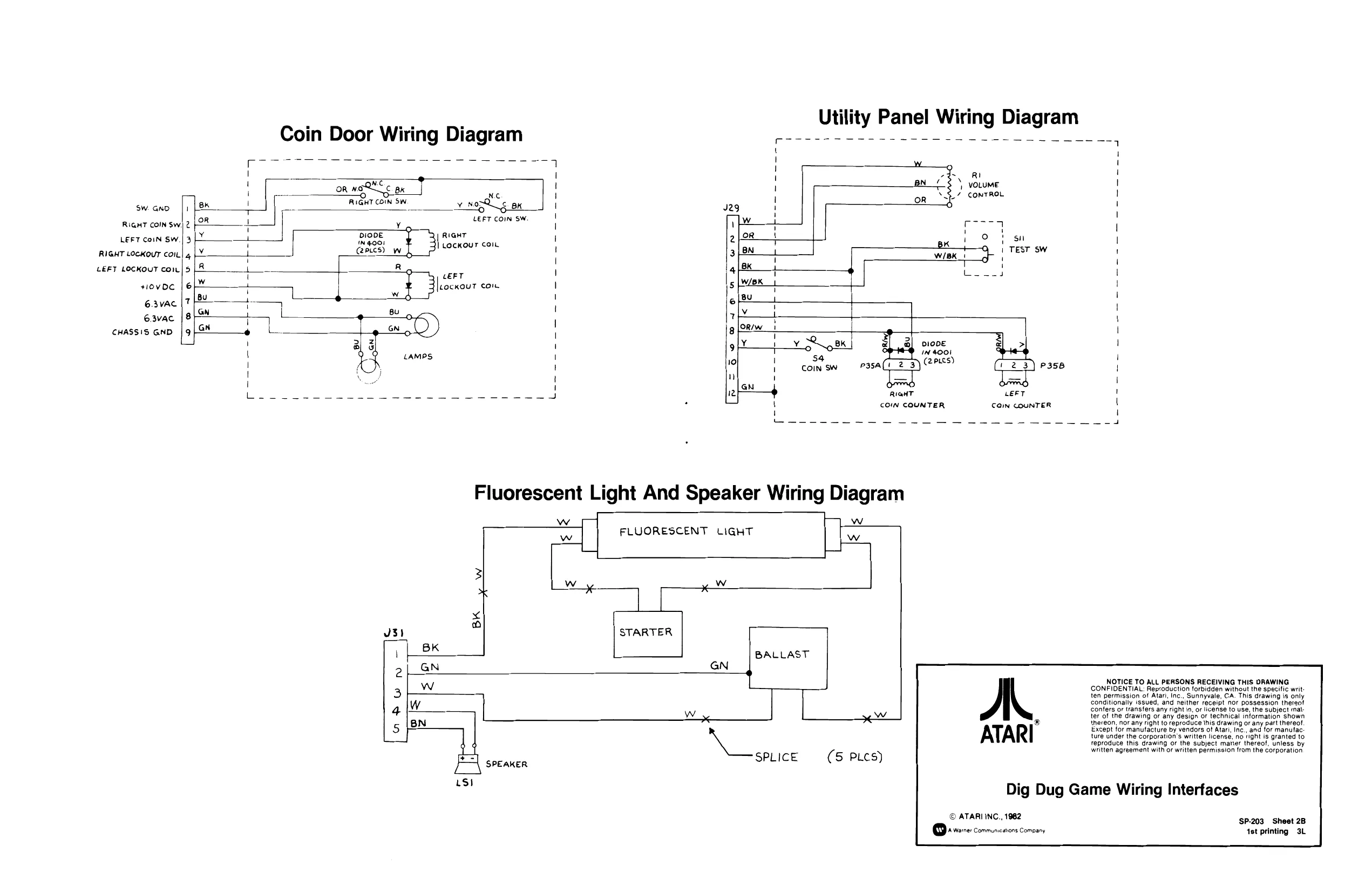
This page is a drawing, shown as the original scan.
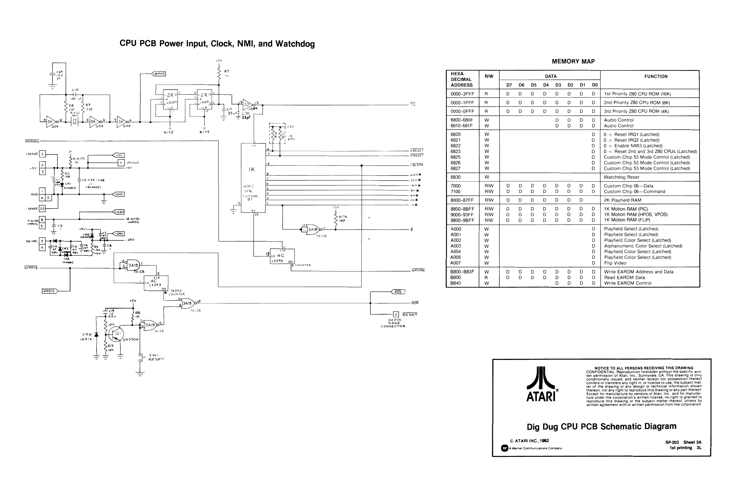
This page is a drawing, shown as the original scan.
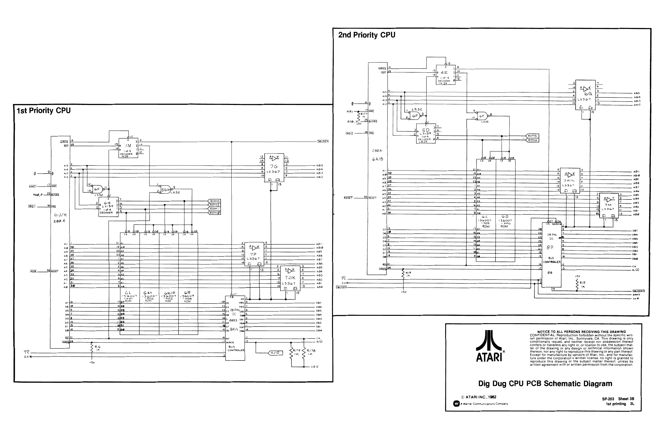
2nd Priority CPU
al uw
1st Priority CPU
is
Seer ele
z a) ls
| | | 2el | ql | ||
| FE tr | 2a] | > | oer | |
| i | 28m | os | ||
| o | oa | ie | ae | ces, |
| al | 25] | fs | ||
| 3 | 2s] | bor |
° a ron
| fat | a! | gp | iB |
is one
| oe | a] | m | ‘be |
| a | Bus | 2. | Be |
contmouen
ATARI
Dig Dug CPU PCB Schematic Diagram
NOTICE TO ALL PERSONS RECEIVING THIS DRAWING CONFIDENTIAL: Reproduction forbidden without the specific writ ten permission of Atari, Inc.. Sunnyvale, CA. This drawing is only conditionally issued, and neither receipt nor possession thereof confers or transfers any right in, or license to use, the subject mat ter of the drawing or any design or technical information shown thereon, nor any right to repreduce this drawing or any part thereot Except for manufacture by vendors of Atari, Inc., and for manutac ture under the corporation's written license, no right is granted to reproduce this drawing or the subject matter thereof, unless by written agreement with or written permission from the corporation
SP-203 Sheet 3B 1st printing 3L
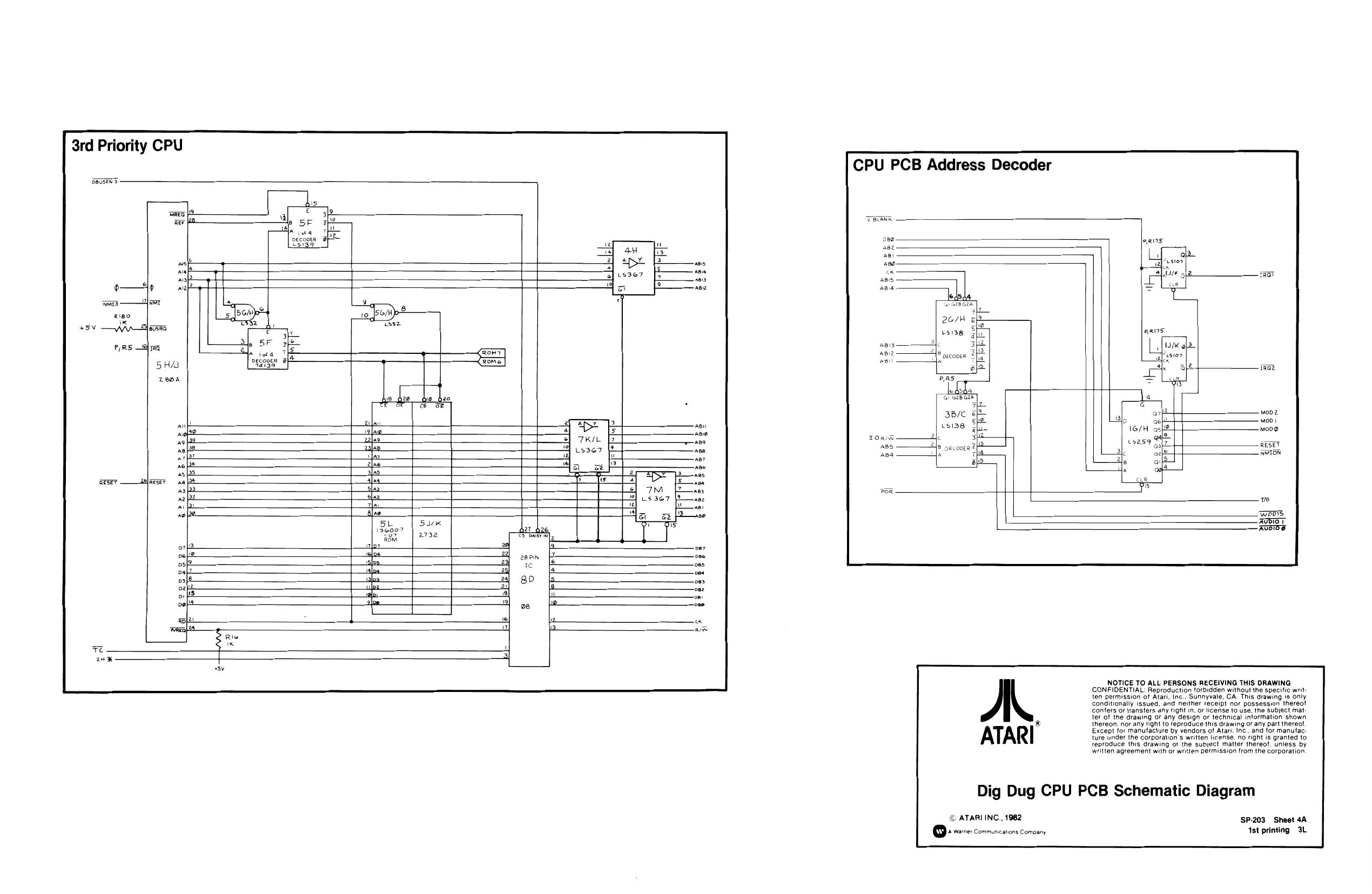
This page is a drawing, shown as the original scan.
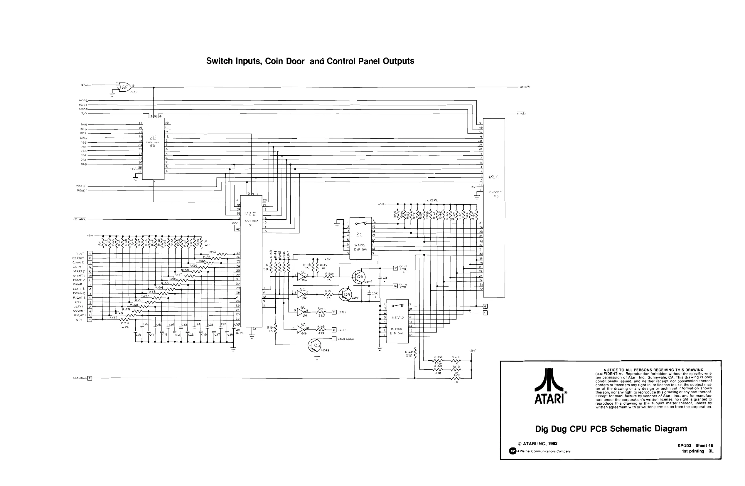
This page is a drawing, shown as the original scan.
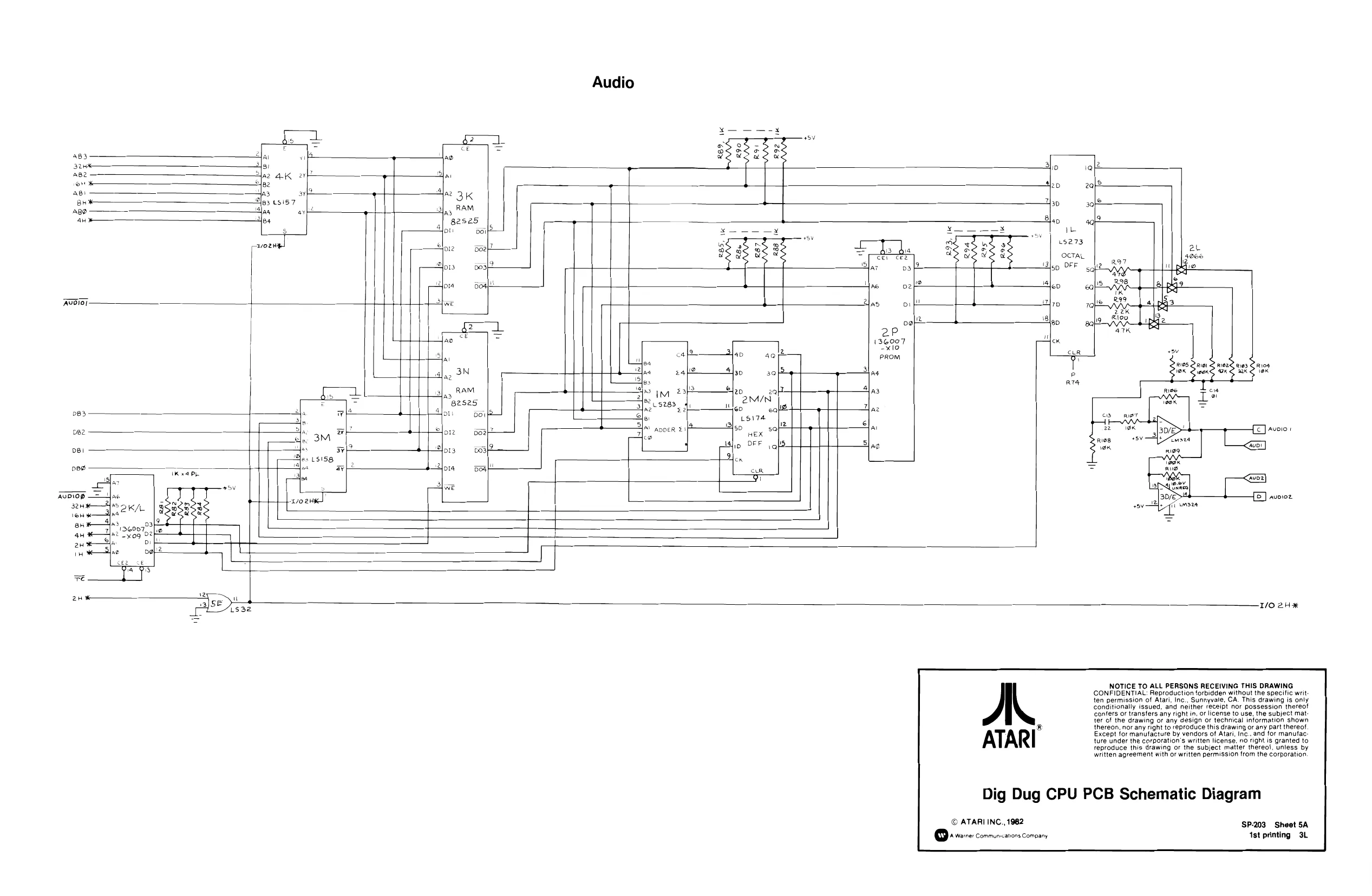
This page is a drawing, shown as the original scan.
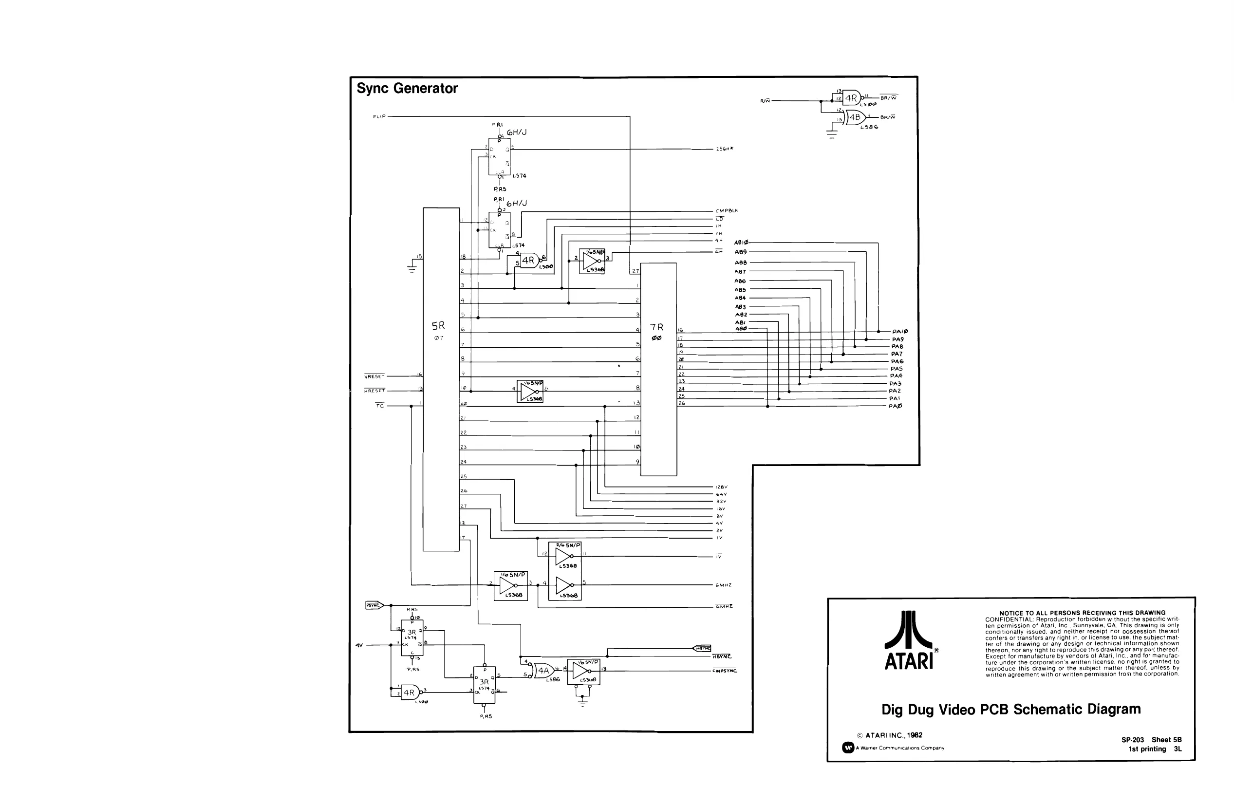
This page is a drawing, shown as the original scan.
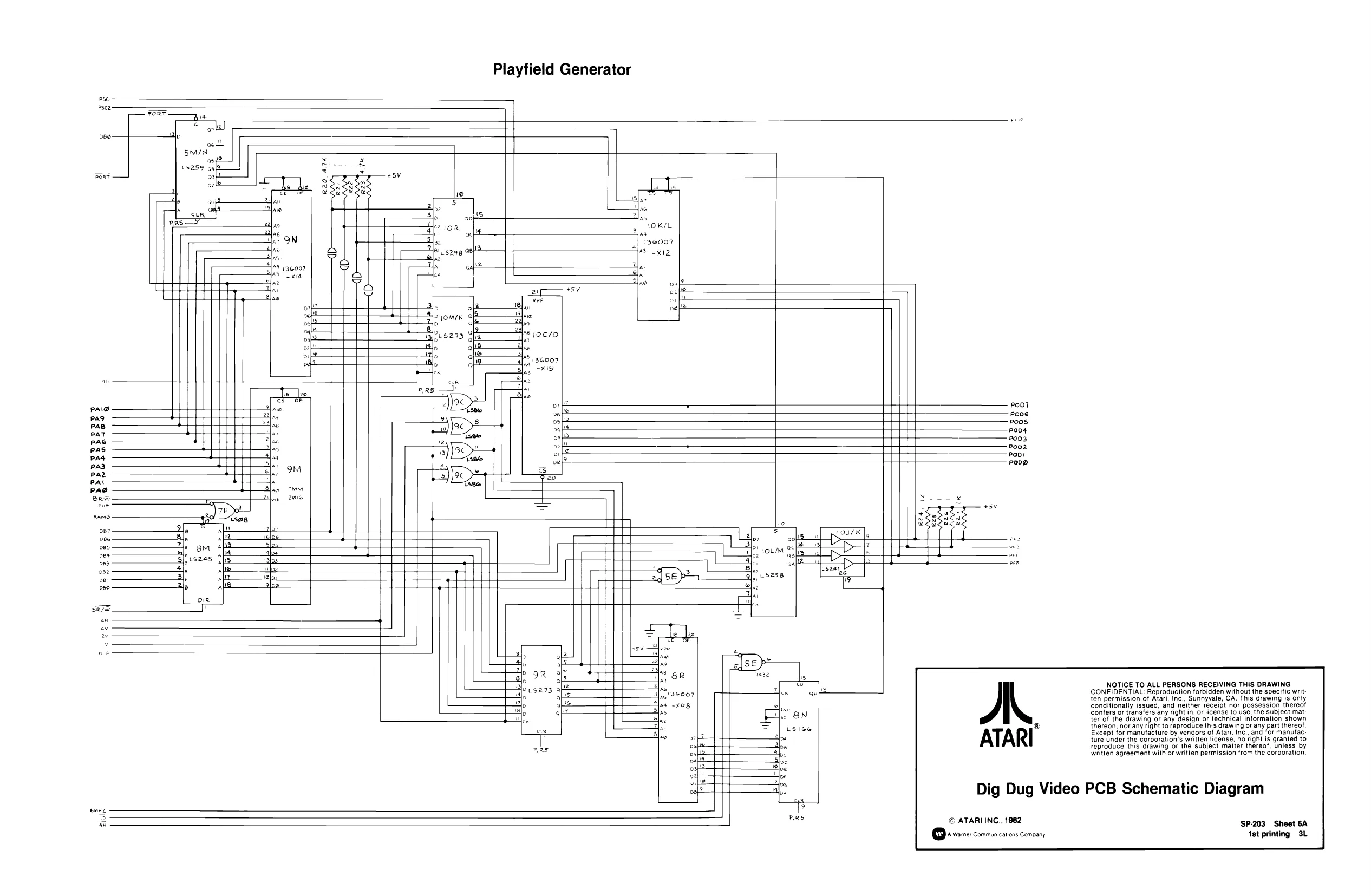
This page is a drawing, shown as the original scan.
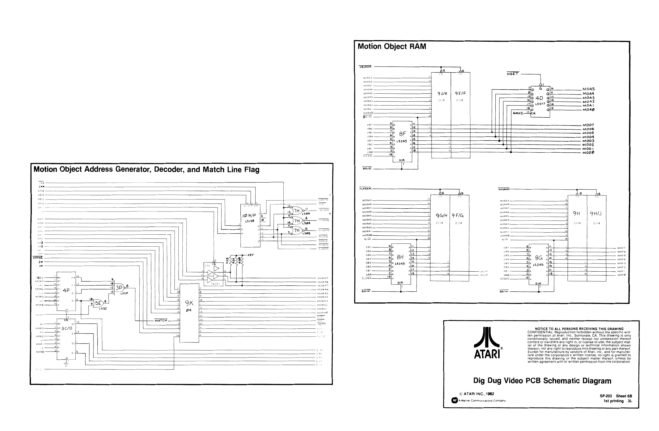
Motion Object RAM
Baw
oes eee a1
Motion Object Address Generator, Decoder, and Match Line Flag
Posnam
sonar
peed
be ho foo Le lan or [foo po SSPE SSS Te] a}
Ray
oey ——a]
confers or transfers any right in, or license to use, the subject mat:
NOTICE TO ALL PERSONS RECEIVING THIS DRAWING CONFIDENTIAL: Reproduction forbidden without the specific writ ten permission of Atari, Inc., Sunnyvale, CA. This drawing is only Conditionally issued, and neither receipt nor possession thereof
ter of the drawing or any design or technical information shown
® thereon, nor any right to reproduce this drawing or any part thereof,
Except for manutacture by vendors of Atari, inc., and for manufac. ture under the corporation's written license, no right is granted to feproduce this drawing or the subject matier thereof, unless by written agreement with or written permission from the corporation.
Dig Dug Video PCB Schematic Diagram
© ATARI INC., 1982 SP-203 Sheet 6B Qe vere: Communications Company 4st printing 3b
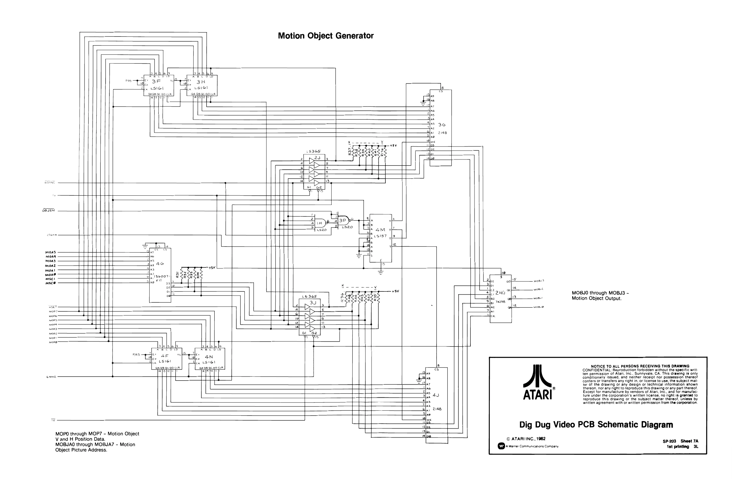
This page is a drawing, shown as the original scan.
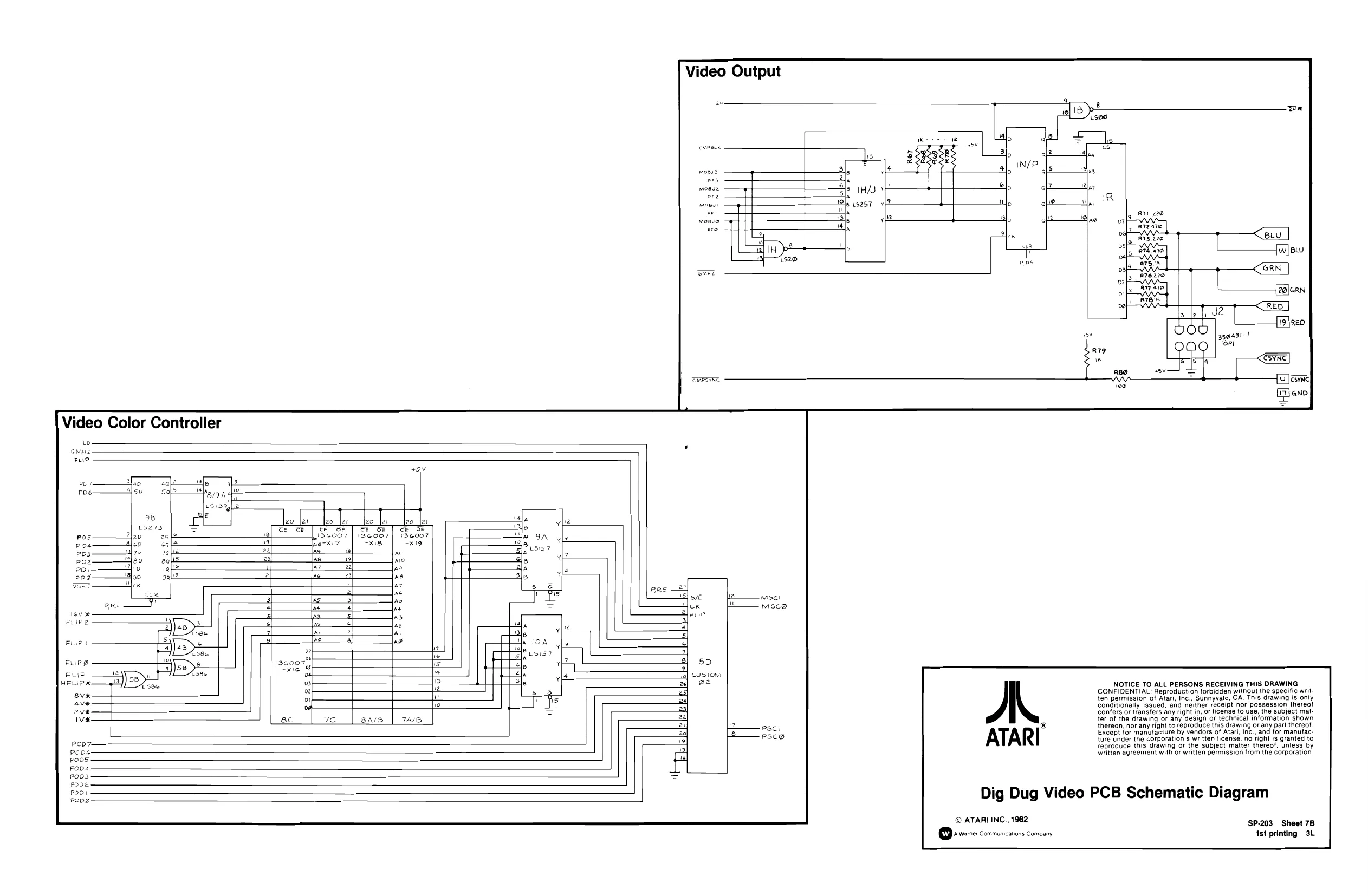
Video Output
RU 220 ao ree. 14 7 RTS jg Ar3tee cin os} ; Epa) aS pre mee owe ost + GRN a 3 RI6220 otf AAS Ad Zalean 1 RBI
Video Color Controller
a
Fup
| Te | OE | te | OF | ce | Se | ce | OF | te |
| 13c007| | t3c007 | Hy | 9a | lo | ||||
| -KI8 | -KI9 | 12lp, | ‘| |
a {ys 5157
| Ao, | L | ele, | 1 |
a2 Pal A a6 B |
- «0 3 <| re an 1 ne
| Fur 28 | a | eS | 10K | Is | a |
136007, A 2} =))58 00% 50
confers or transfers any right in, or license to use, the subject mat. ter of the drawing or any design or technical information shown NOTICE TO ALL PERSONS RECEIVING THIS DRAWING CONFIDENTIAL: Reproduction forbidden without the specific writ ten permission of Atari, Inc., Sunnyvale, CA. This drawing is only Conditionally issued, and neither receipt nor possession thereot
® thereon, nor any right to reproduce this drawing or any part thereo! Except for manufacture by vendors of Atari, Inc., and for manufac: ture under the corporation's written license. no right is granted to reproduce this drawing or the subject matter thereof, unless by written agreement with or written permission from the corporation.
Dig Dug Video PCB Schematic Diagram
© ATARI ING., 1982 5P.263y Sheoi,78 + were: Communications Company 1st printing 3L
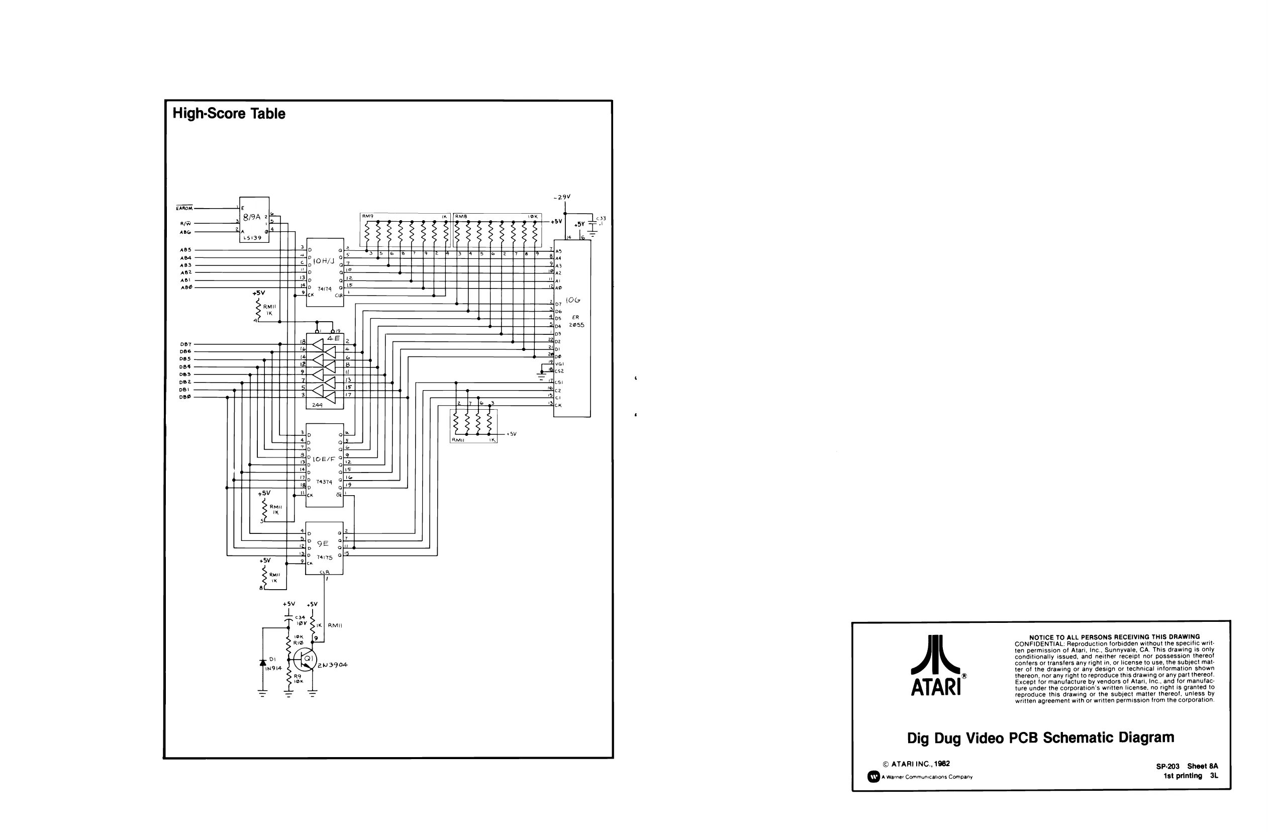
This page is a drawing, shown as the original scan.
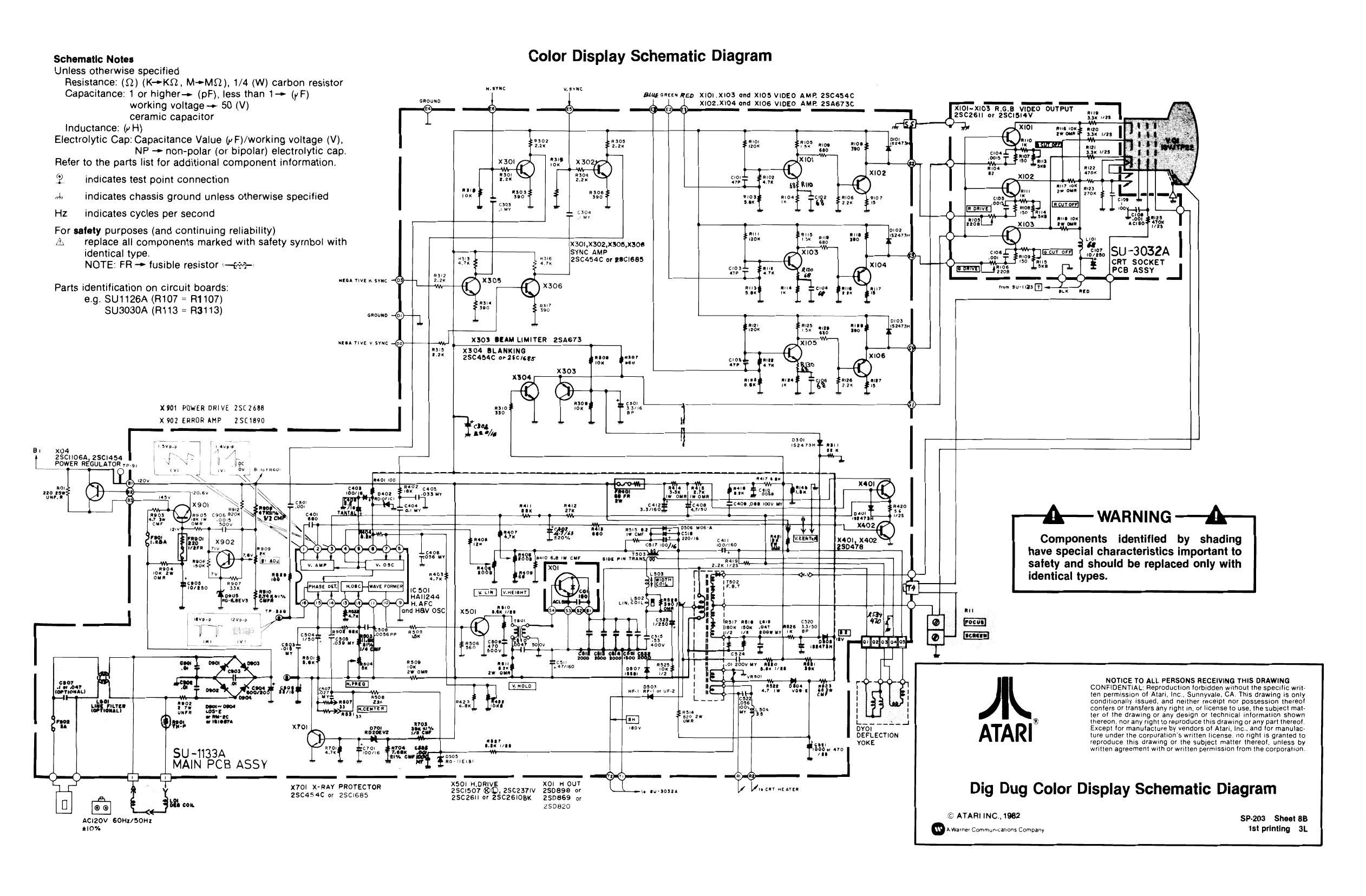
Schematic Notes Unless otherwise specified Resistance: (Q) (K-*K2, M*MQ), 1/4 (W) carbon resistor Capacitance: 1 or higher (pF), less than 1-> (yF) working voltage > 50 (V) ceramic capacitor Inductance: (/ H) Electrolytic Cap: Capacitance Value (y F)/working voltage (V), NP — non-polar (or bipolar) electrolytic cap. Refer to the parts list for additional component information.
2 indicates test point connection ih indicates chassis ground unless otherwise specified Hz __ indicates cycles per second For safety purposes (and continuing reliability) aA replace all components marked with safety syrnbol with identical type.
Parts identification on circuit boards: e.g. SU1126A (R107 = R1107) SU3030A (R113 = R3113)
X901 POWER DRIVE 2SC 2686
X902 ERROR AMP 2SC1890
Color Display Schematic Diagram
Blug sREEN RED XI01.X103 and XIO5 VIDEO AMP. 2SC454C X102.X104 and X106 VIDEO AMP. 2SA673C
SYNC AMP. 2SC454C or BBCi6as
ween tive v s¥Ne G5
x94 2SCI106A, 28C1454 Sf /\ POWER REGULATOR ro.9, VN Toe X303 BEAM LIMITER 2SA673 X304 BLANKING 25C454C or 26C/6es
x304 noe
xloz
ope pe
X301,X302,X80B,x308
26754 2SC26I! or BSCIsI4V Xl0l~XI03 R.G.B VIDEO OUTPUT aus 1 BSc ves
ICRT SOCKET PCB ASSY _I
he ae
nee Ea Ie tn 7 cre
X01 edeivee
hae |
SU -1133A MAIN PCB ASSY
ACI20V 60H2/50Hz 210% X50! H.ORIVE XO H OUT 2SCi507 BL, 2sc2z371v 280898 or 2SC26II or ZSCZEIOBK 250869 or X70 X-RAY PROTECTOR 2SC454C or 25C1685
280820 YOKE | NE ay yor DEFLECTION A.
ATARI
WARNING
Components identified by shading have special characteristics important to safety and should be replaced only with identical types.
NOTICE TO ALL PERSONS RECEIVING THIS DRAWING CONFIDENTIAL: Reproduction forbidden without the specitic writ ten permission of Atari, Inc., Sunnyvale, CA. This drawing is only conditionally issued, and neither receipt nor possession thereof confers or transfers any right in, or license to use, the subject matter of the drawing or any design or technical information shown thereon, nor any right to reproduce this drawing or any part thereof. Except for manufacture by vendors of Atari, Inc., and for manulac. ture under the corporation's written license. s10 right is granted to reproduce this drawing or the subject matter thereof, unless by written agreement with or written permission from the corporation.
Dig Dug Color Display Schematic Diagram
‘SP.203 Sheet 8B 1st printing 3L