Lunar Lander DP-136-3rd-02A
Lunar Lander (rev 2) (Atari, 1979) · Drawing Package · 1 pages · original scan
MPU CIRCUITRY ADDRESS DECODING CIRCUITRY
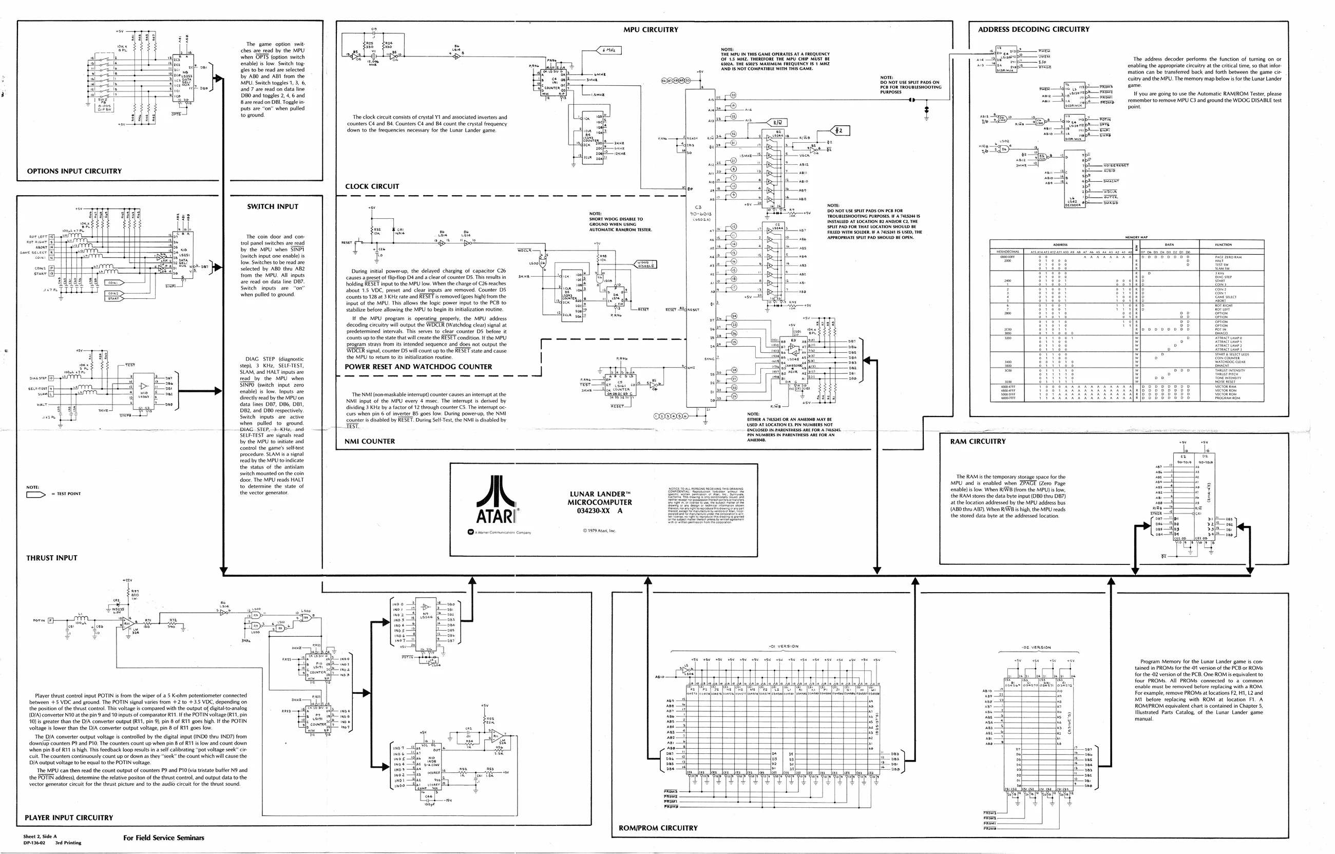
‘The game option swit ches are_read by the MPU when OPTS (option switch tenable) is low. Switch tow: ales to be ead are selected bby ABO and ABI from the MPU. Switch toggles 1,3. 6 ro nore {Tat MPU Iv Tas GAME OnERATES AT ‘Sona tae says waxiMune#ReQUS The adétess decoder performs the function of turning on oF enabling the appropriate circuitry atthe critical time, so that infor ‘mation can be transfered back and forth between the game cit
culty and the MPU. The memory map below is fr the Lunar Lander
DO Nor Use sptit PADS ON
| Lil | sell peor iy | Feo vox movstlsnoorne | fame. |
i Bo seecwated Fonroses HF you are going to use the Automatic RAMROM Tester, please Fatale p ae o ‘remember to femove MPU C3 and ground the WOOG DISABLE test puts are “on hen pulled : an. fo ground The clock cuit consists of crystal Y1 and associated inverters and = e counters C4 and Ba. Counters C4 and B4 count the ental frequency down fo the frequencies necessary forthe Lunar Lander game,
cmeey
OPTIONS INPUT CIRCUITRY
CLOCK CIRCUIT eo
7 a
| SWITCH INPUT | ~~ | Do nor use str paps on ce tox |
Not woos owas 10 Instat Ar location 82 AxD)08 Ce
| ac | et | ‘tUronane mawiron st | srr von ar ocaton UND ae | ||||||
| sorter | The coin door and con- | Shee | Irekomint sr | 4D SHOULD B& FEN | sansa | ||||
| Besnad | tual panel switches ae oad | woop | opt | pe | 7 | = | — | ||
| come sexecr fa | by the MPU when SINPI | TD | Te | a | a | al | ee eee | ||
| aa | low. Switches to be read are | ¥ | “ | sra8e | : | ° | ists | ||
| sx | aelecindby. ABO eu ABR | During inal powecup, the delayed charging of capacitor C26 | gig | ‘ | sit | ||||
| soar | from the MPU. Al inputs | causes. a preset of lipflop DA anda clear of counter DS. This results in | $3 | HA | #4 | ||||
| ate read on data tne DB, | hing RESET input to the MPU low: When the charge of C26 reaches | HE | BAH | ||||||
| Switch inputs ae | “on | about 15 VOC. preset and clear inputs are removed, Counter DS | 7 | ore | Te | ||||
| when pulled to ground | ‘Counts o 128 at 3 Riz rate and RESET i removed (goes high fom the | : | is | HH | |||||
| input of the MPU. This allows the logic power input to the PCB to | $ | gig | eee | in | |||||
| Stablize before allowing the MPU to begin i | nialzation routine. | rr Aecaer | ZL | tie | SnAg | a | Bie | ||
| I the MPU program | operating properly, the MPU address | Tee | Tope | a | Orne | ||||
| decoding cuir will output the WDCER (Watchdog clay signal at | Sighs | aye | $3 | ist | |||||
| predetermined intervals. Ths serves to clear counter DS before | = | gitin, | glpcecoods | ao | |||||
| ‘Count up to the stat that wil create the RESET condition, Ifthe MPU | SSS oe | ee | = | aera | = | ||||
| ‘rogram strays from its intended sequence and does not output the | siise | * | ° | ‘Rnact vw > | |||||
| c | WDCIR signal, counter DS will count upto the RESET state and cause | ae | rg | a | Sen ete OT | ||||
| DIAG. STEP agnostic | tee MPU tam | Re lltoation eae | | | un | , | cor | a | ae" | |
| step) | 3 KH, SELPTEST, | POWER RESET AND WATCHDOG COUNTER | dunt | ® | peels | = | pitted | 2 | Bey |
| read by the MPU when | = | — | « | wo) | ‘i | giiiis | Hi | ane, | |
| SINFO (switch input zero | FS co | a | ae, | seo | SE RSUSESCCSES 8 eee | ror | |||
| pov —ileg Sate | ee | as -O | Fok | ar | Testa | Aaasaaaadel see bsae | Weror tow | ||
| deectyrecdby ba NOU on | NMI input of the MPU every 4 msec. The interrupt i derived by | fee | LE | | oe |
data lines DB, DBS, DB viding Kitz by a actor of 12 trough counter Co. The tert oc
| 2, | and | DBO | respectively. | us when pin 6 of inverter | BS goes tow. During powerup, the Nba | 69080 | Now. |
| itch | inputs | ace active | ounte i dsabed by | RESET. During Self Test, the NMI is disabled by | ERR A 714085 On AN anon MAYBE | ||
| 10. ground | a | + | {ato at vocanion tr NUMBERS NOT | ||||
| ee | Stera-ktlg and | [| | TEST. | ——— | INCLOMD PARENTS ARE TOR | 8A |
SELETEST are signals read br ns nents at YOR AN =
by the MPU to inate and NMI COUNTER nese RAM CIRCUITRY sony
conto the game’ etext Lk procedure, SLAM i signal ead by the MPU to indicate the status of the antislam switch mounted on the coin door, The MPU reads HALT to determine the state of the vector generator.
“The RAM isthe temporary storage space forthe
MPU and is enabled when ZPAGE (Zero Page tenable) is low When ROWE (from the MPU) slow, the RAM stores the data byte input (OBO they DB?) atthe location addressed by the MPU address bus (80 thru AB?) When RIWBis high, the MPU reads the stored data byte at the addressed location CS -tsrronr canes) A. LUNAR LANDER™ Sekh eeeer es I MICROCOMPUTER ete cetaenaee ATARI" 034230-XX A Seon
THRUST INPUT
pct Program Memory for the Lunar Lander game is con-
tained in PROMS for the-01 version of the PCB or ROMS
for the-02 version ofthe PCB. One ROM is equivalent to four PROMs. All PROM: connected toa. common tenable must be removed before replacing with a ROM, For example, remove PROMS at locations F2, HY, L2 and Mi before replacing with ROM at location FI. A ROM/PROM equivalent chart is contained in Chapter 5, Mlustrated Parts Catalog, of the Lunar Lander game manual L
Player thrust control input POTIN is from the wiper ofa 5 K-ohm potentiometer connected between +5 VDC and ground, The POTIN signal varies from +2 to +35 VDC, depending on the position ofthe thust control. Ths voltage is compared with the output of digital-to-analog (DIA) converter N10 atthe pin 9 and 10 inputs of comparator RUT. Ifthe POTIN voltage R11, pin 10); greater than the DIA converter output (R1, pin 9), pin 8 of R11 goes high. Ifthe POTIN voltage is lower than the D/A converter output voltage, pin 8 of RTT goes low. ‘The DIA converter output voltage is controlled by the digital input (INDO thru IND7) from <downlup counters P3 and P10. The counters count up when pin 8 of R11 is low and count down ‘when pin & of Rit is high. This feedback loop results ina self calibrating “pot voltage seek” ci. ‘uit The counters continuously count up or down as they “seek the count which will cause the D/A output voltage to be equal tothe POTIN voltage. The MPU can then read the count output of counters P9 and PIO (via wstate buffer NB and the POTIN address), determine the relative positon ofthe thrust contro, and output data to the ‘vector generator circuit forthe thust picture and to the audio circuit for the thrust sound.
PLAYER INPUT CIRCUITRY
Sheet 2 Side A For Field Service Seminars
DP.13602 Sd Printing ROMIPROM CIRCUITRY