Quantum SP-221 1st Printing
Quantum (rev 2) (General Computer Corporation (Atari license), 1982) · Schematic Package · 22 pages · 77 sections · original scan
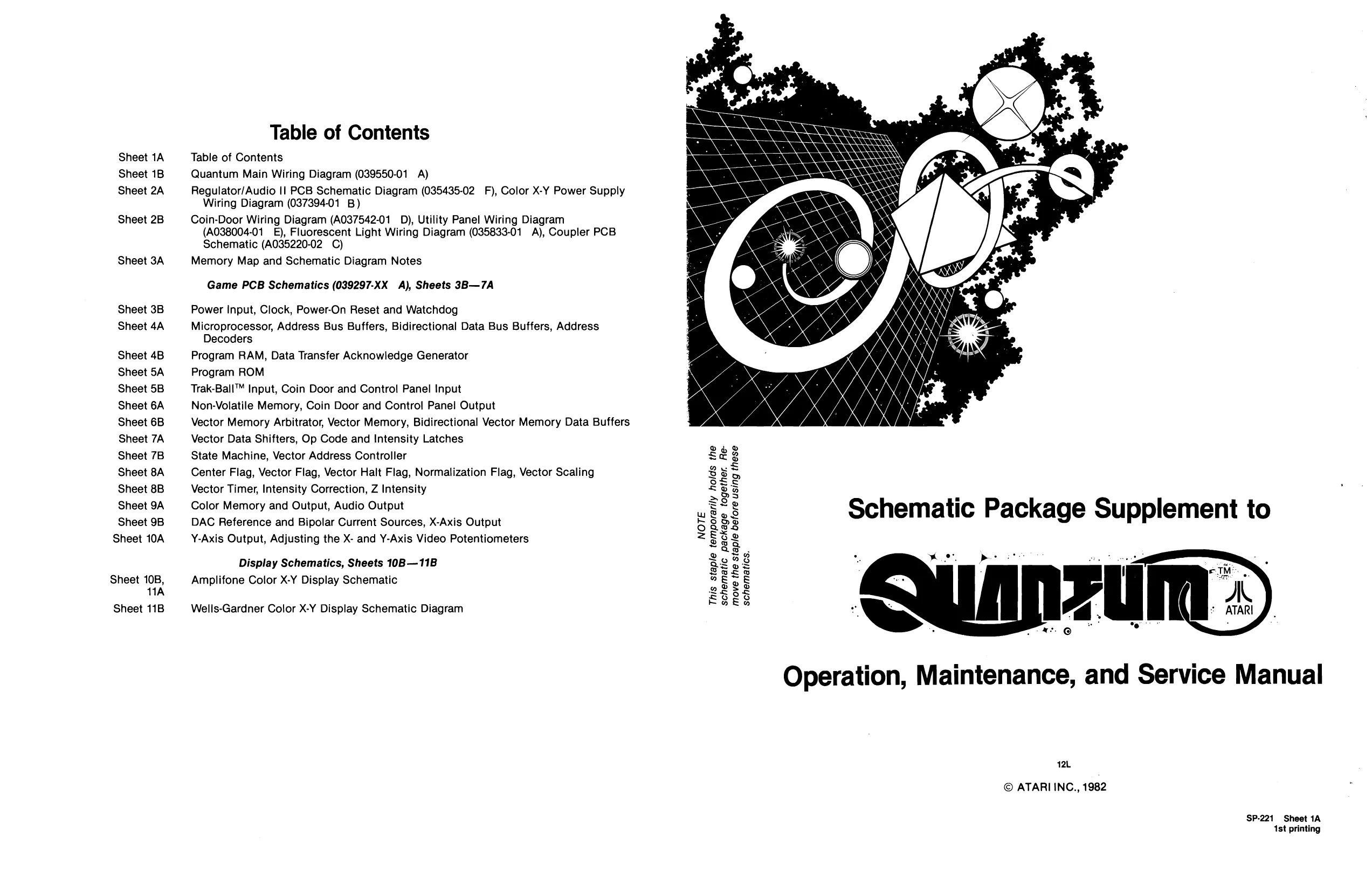
Table of Contents
Sheet 1A Table of Contents Sheet 1B Quantum Main Wiring Diagram (039550-01 A) Sheet 24 Regulator/Audio Il PCB Schematic Diagram (035435-02 F), Color X-Y Power Supply Wiring Diagram (037394-01 B) Sheet 2B Coin-Door Wiring Diagram (A037542-01 D), Utility Panel Wiring Diagram (A038004-01 E), Fluorescent Light Wiring Diagram (035833-01 A), Coupler PCB Schematic (A035220-02 C) Sheet 3A Memory Map and Schematic Diagram Notes
Game PCB Schematics (039297-XX A), Sheets 3B—7A
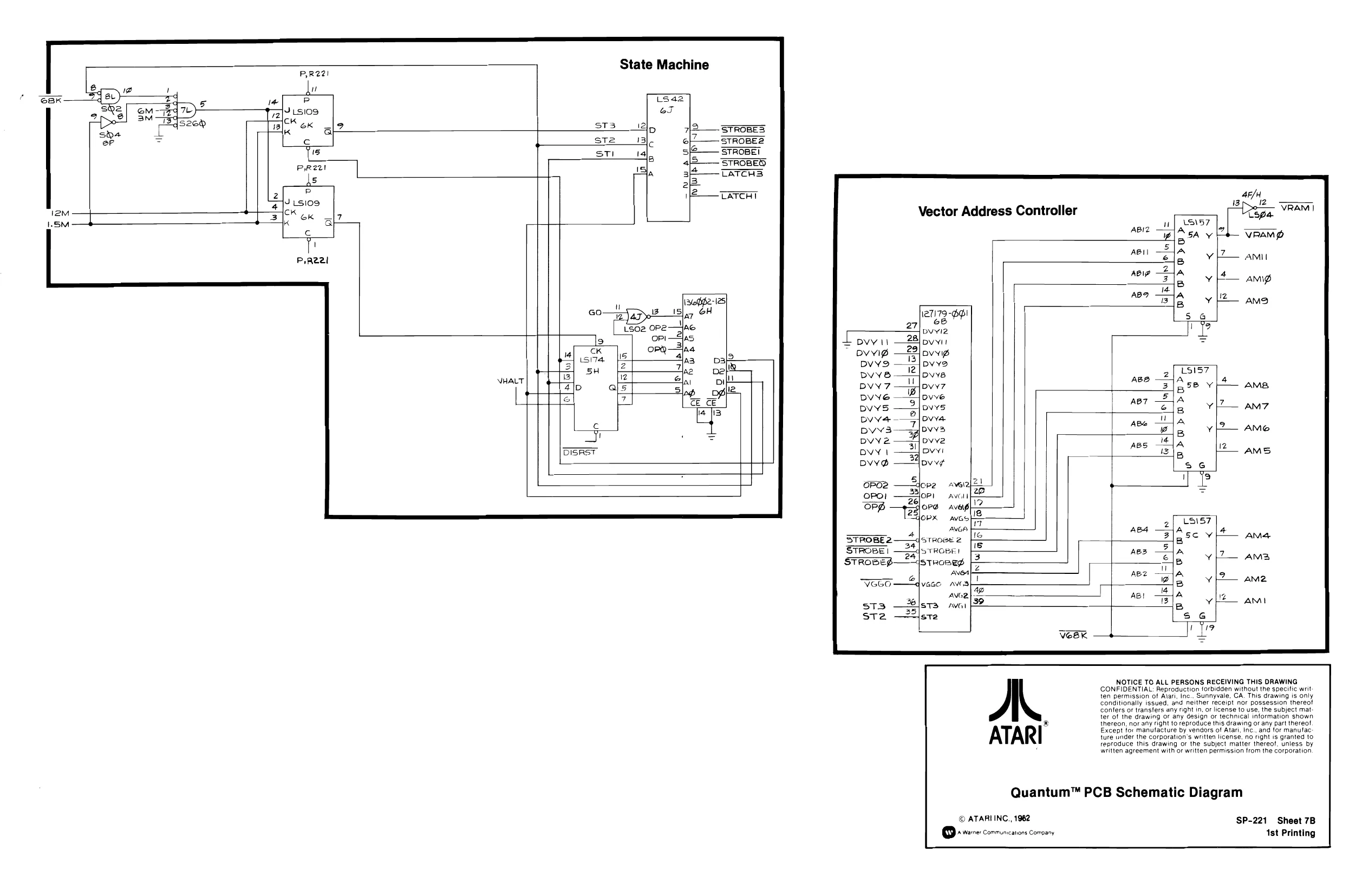
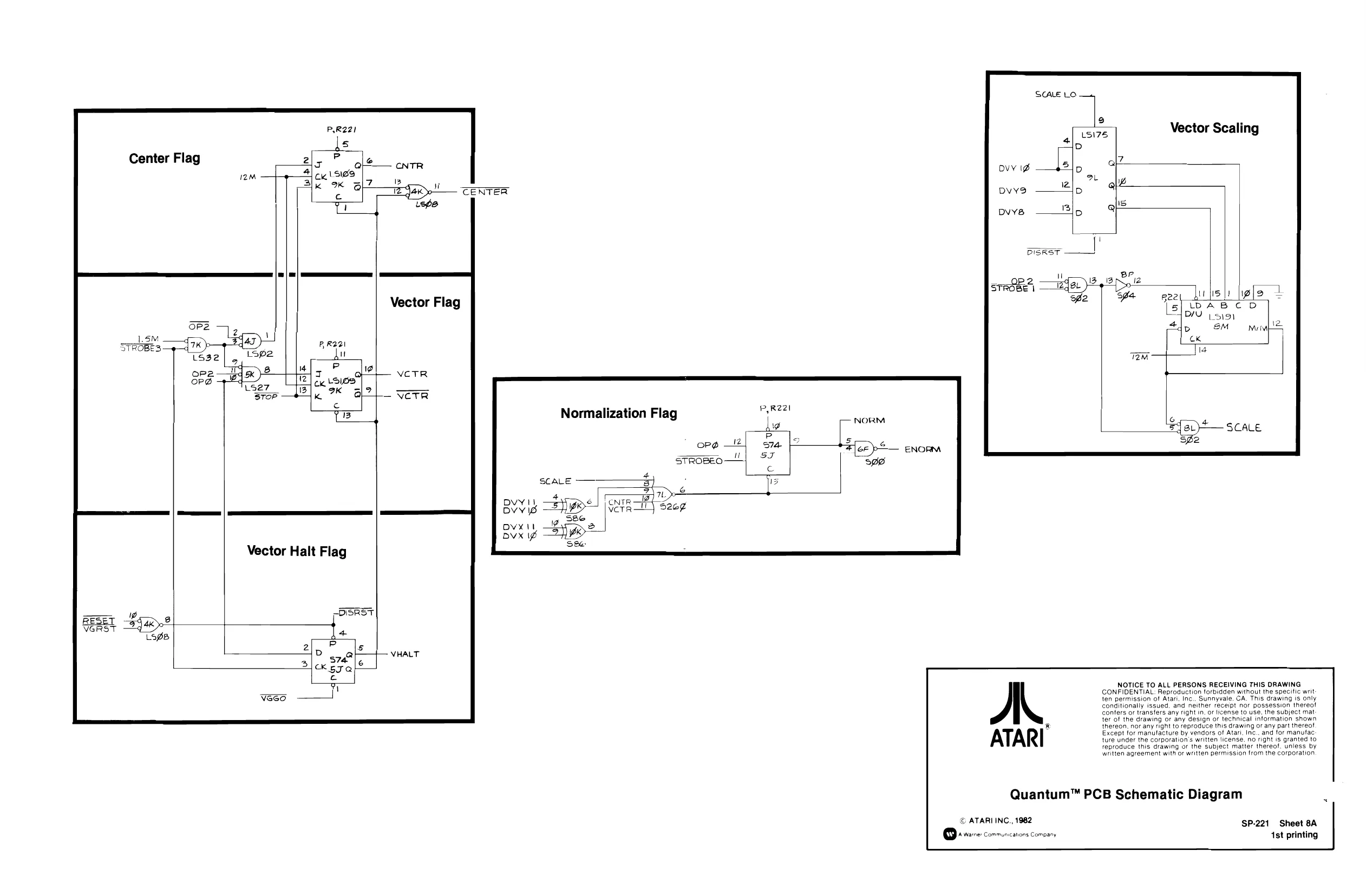
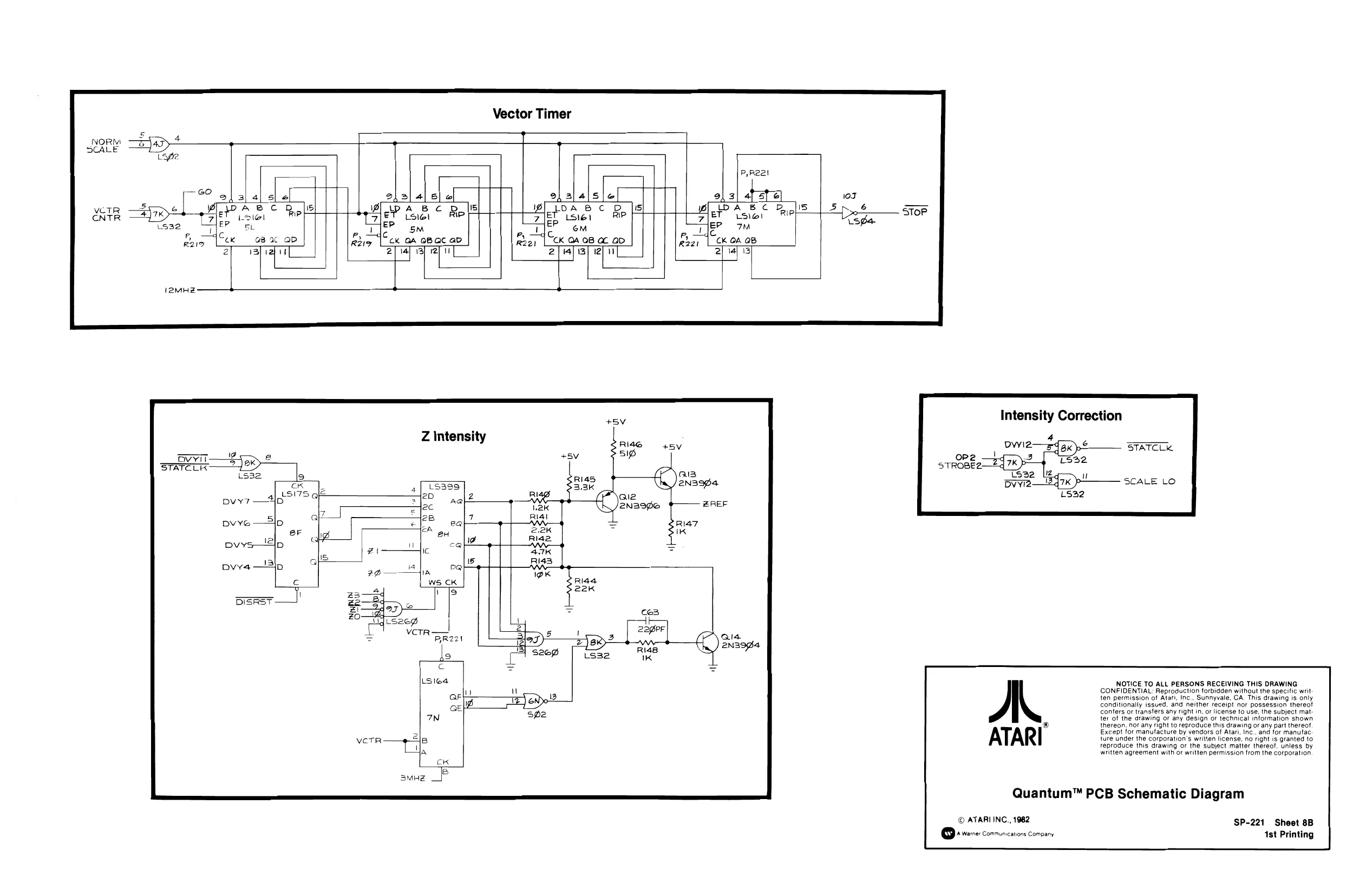
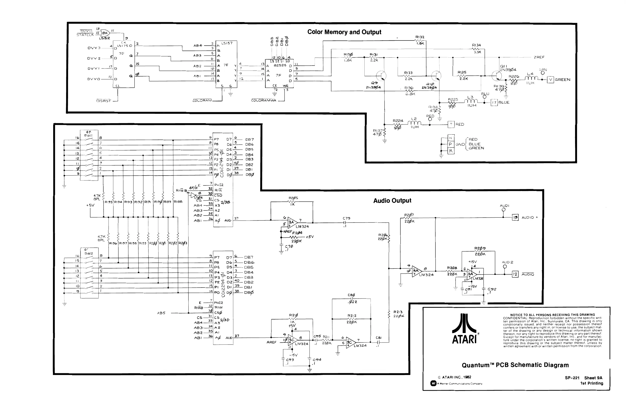
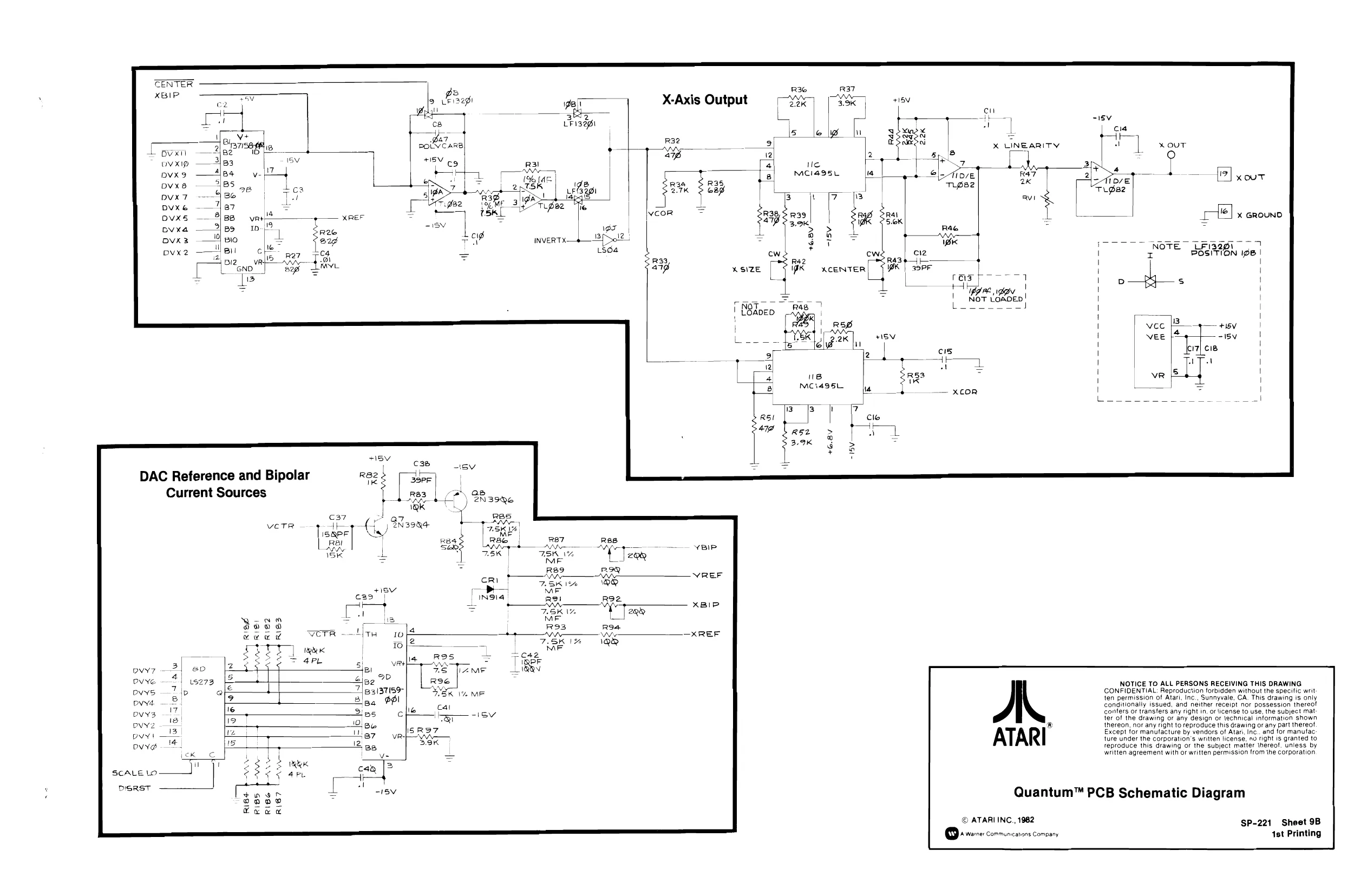
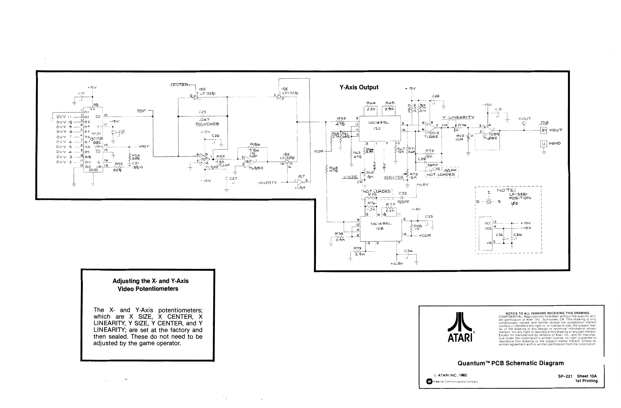
Sheet 3B Power Input, Clock, Power-On Reset and Watchdog Sheet 4A Microprocessor, Address Bus Buffers, Bidirectional Data Bus Buffers, Address Decoders Sheet 4B Program RAM, Data Transfer Acknowledge Generator Sheet 5A Program ROM Sheet 5B Trak-Ball™ Input, Coin Door and Control Panel Input Sheet 6A Non-Volatile Memory, Coin Door and Control Panel Output Sheet 6B Vector Memory Arbitrator, Vector Memory, Bidirectional Vector Memory Data Buffers Sheet 7A Vector Data Shifters, Op Code and Intensity Latches Sheet 7B State Machine, Vector Address Controller Sheet 8A Center Flag, Vector Flag, Vector Halt Flag, Normalization Flag, Vector Scaling Sheet 8B Vector Timer, Intensity Correction, Z Intensity Sheet 9A Color Memory and Output, Audio Output Sheet 9B DAC Reference and Bipolar Current Sources, X-Axis Output Sheet 10A Y-Axis Output, Adjusting the X- and Y-Axis Video Potentiometers
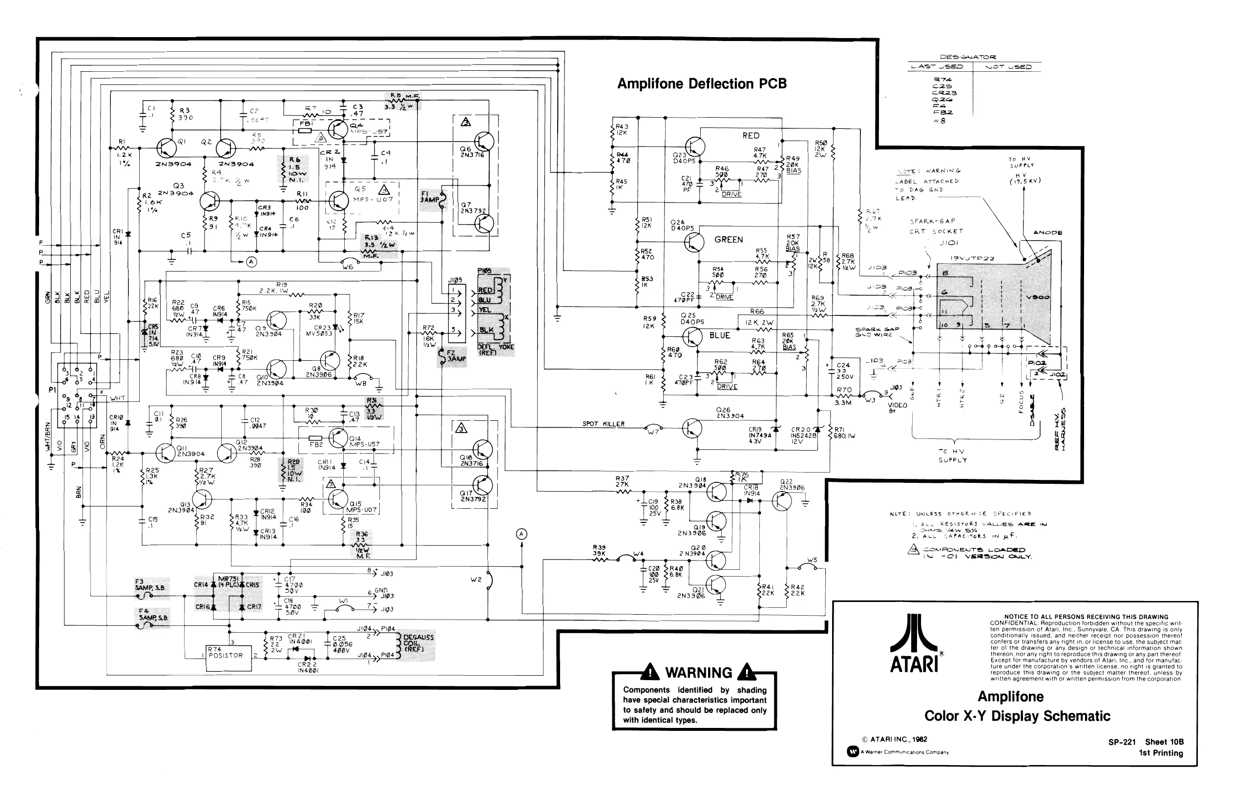
Display Schematics, Sheets 10B—11B Sheet 10B, Amplifone Color X-Y Display Schematic 1A Sheet 11B Wells-Gardner Color X-Y Display Schematic Diagram move the staple before using these schematic package together. Re-
schematics.
Operation, Maintenance, and Service Manual
12L
© ATARI INC., 1982
SP-221 Sheet 1A 1st printing
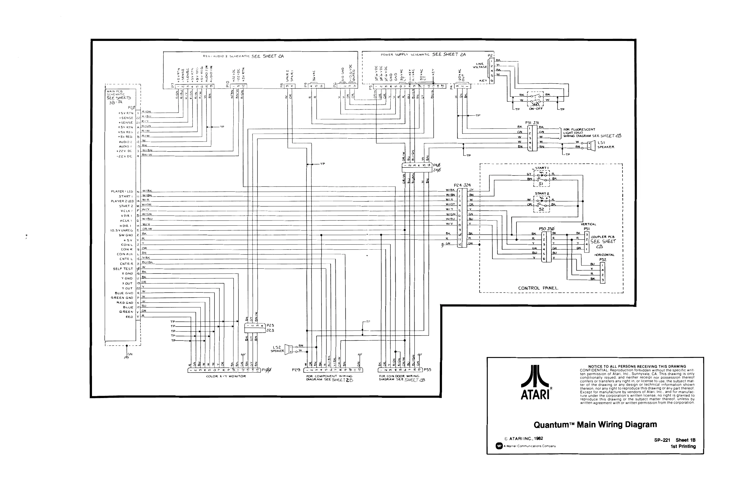
This page is a drawing, shown as the original scan.
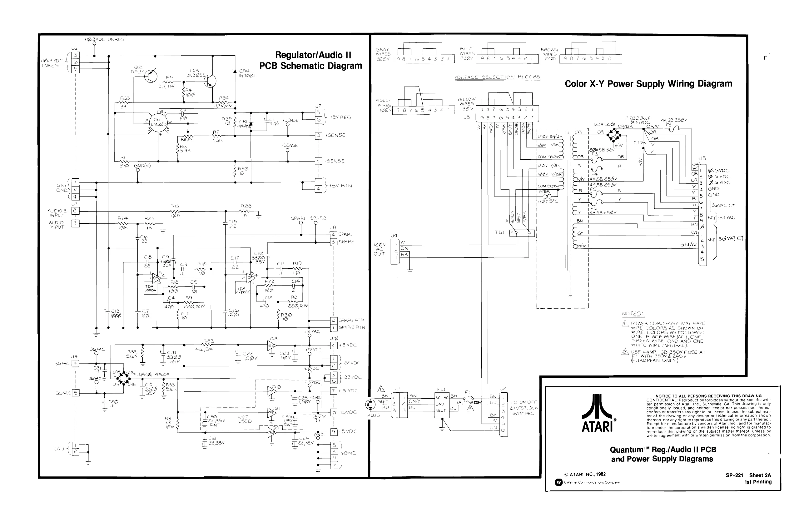
tID BVOC UNREG
BROWN pave Regulator/Audio I! Lead ace ecw. wie UNF cag PCB Schematic Diagram INFDDE
YELLOW WIRES l2Ov
+SENS. 2 7POOut BeNSE —-4asB esav Fe
R) c e272 OND(2) T Ledv ven |idov wer is J
P.wVOC \P voc 1D VOC GND GND
Sevac CT
Key Wo (VAC 4uDI02 NPUT AUDIO | INPUT BOOS UPN
xey| SB VAT CT
20, "ew 22G,tew| aul i R20 TES SPARI AT A COR bias DOWER CORD ASSY MAY HAVE SPKRE RTN WiRE ORS AS SHOWN OR WIRE COLORS 45 FOLLOWS . 4 ONE BLACK WIRE (AC), ONE aoe GREEN WIRE GND AND ONE + WwW WHITE WIRE (NEUTRAL). USE 4aMP, SB 250V FUSE AT Be 8 < “FT WiTH 220V6 e40v 3g¢ (EUROPEAN ONLY) + nae 4PLcs AMecas 73308 $5 NOTICE TO ALL PERSONS RECEIVING THIS DRAWING CONFIDENTIAL: Reproduction forbidden without the specitic writ: ten permission of Atari, Inc., Sunnyvale, CA. This drawing is only Conditionally issued, and neither receipt nor possession thereot confers or transfers any right in, or license to use, the subject mat ter of the drawing or any design or technical information shown
thereon. nor any right to reproduce this drawing or any part thereot
Except for manufacture by vendors of Atari, Inc. and for manutac: ture under the corporation's written license, no night is granted to reproduce this drawing or the subject matter thereof. unless by written agreement with or written permission from the corporation,
ND Y ; 5} Quantum™ Reg./Audio II PCB
and Power Supply Diagrams
¢ iT 22,35v
© ATARI INC., 1962 SP-221 Sheet 2A
tw warner Commurscations Company ‘4st Printing
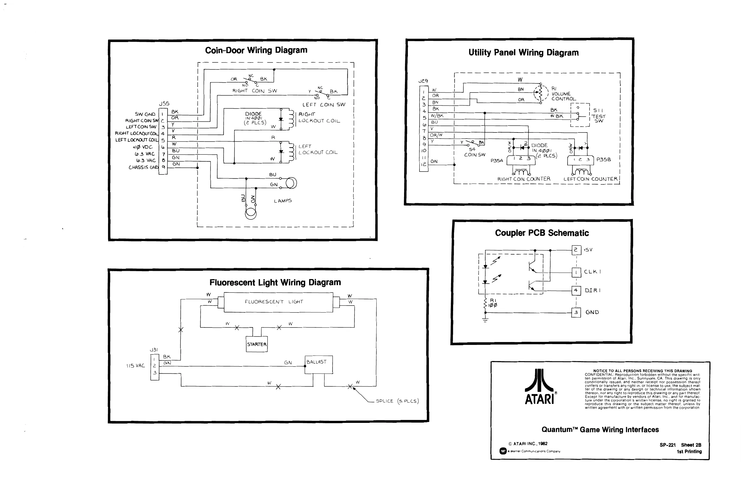
This page is a drawing, shown as the original scan.
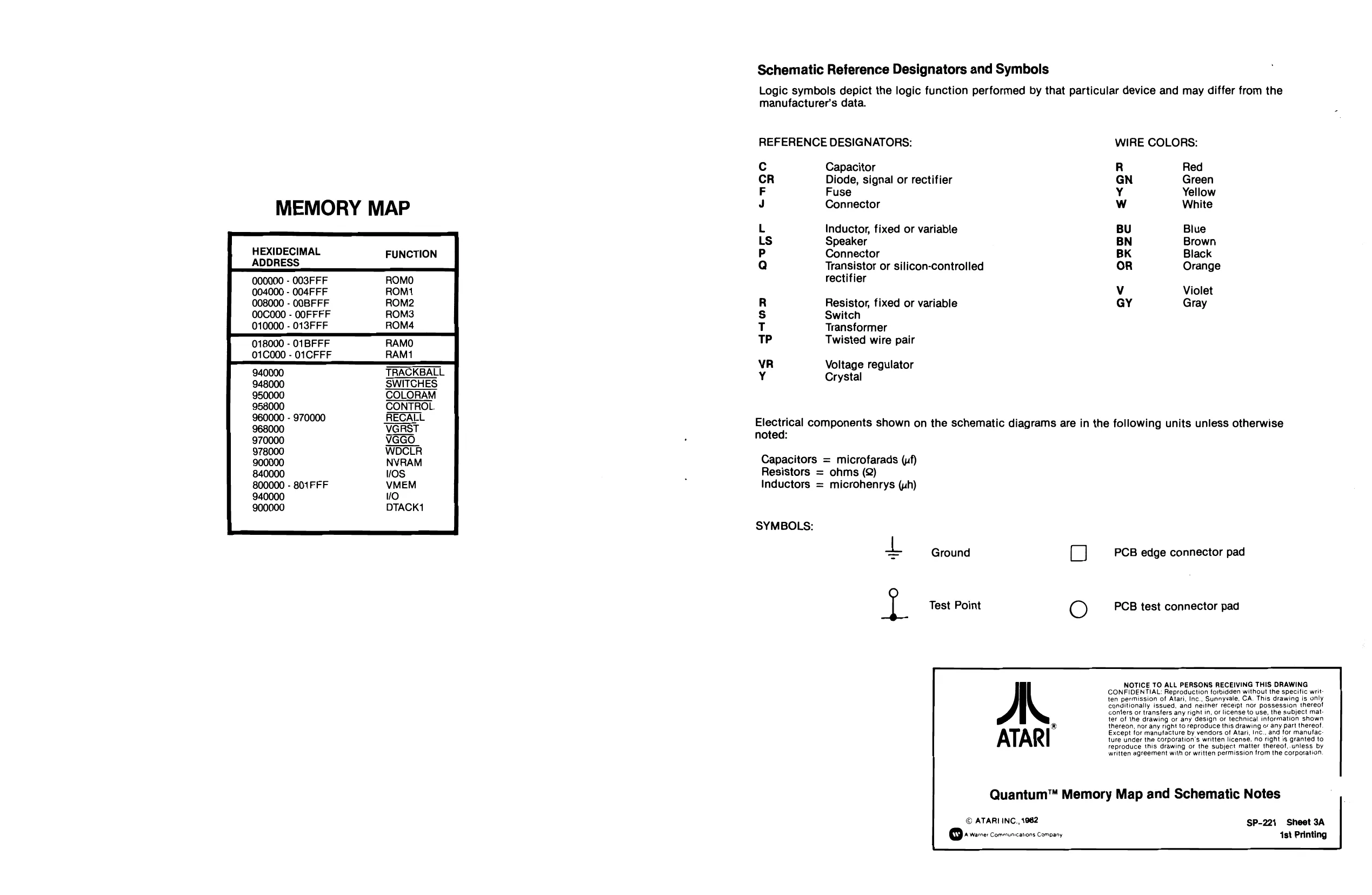
Schematic Reterence Designators and Symbols
Logic symbols depict the logic function performed by that particular device and may differ from the manufacturer's data.
REFERENCE DESIGNATORS: WIRE COLORS:
c Capacitor R Red
| CR | Diode, signal or rectifier | GN | Green |
| F | Fuse | Y | Yellow |
MEMORY MAP J Connector Ww White
| L | Inductor, fixed or variable | BU | Blue |
LS Speaker BN Brown
HEXIDECIMAL FUNCTION P Connector BK Black
ADDRESS Qa Transistor or silicon-controlled OR Orange
000000 - 003FFF rectifier
| 004000 - OO4FFF | v | Violet | ||
| 008000 - OOBFFF | R | Resistor, fixed or variable | GY | Gray |
| 00C000 - OOFFFF | s | Switch | ||
| 010000 - 013FFF | T | Transformer | ||
| 018000 - 01BFFF | TP | Twisted wire pair |
01000 - 01CFFF Voltage regulator Crystal << D TRACKBALL SWITCHES COLORAM
Electrical components shown on the schematic diagrams are in the following units unless otherwise noted:
Capacitors = microfarads (uf) Resistors = ohms (&) Inductors = microhenrys (uh)
SYMBOLS: L Ground oO PCB edge connector pad
Test Point oO PCB test connector pad
NOTICE TO ALL PERSONS RECEIVING THIS DRAWING CONFIDENTIAL: Reproduction forbidden without the specific writ ten permission of Atari, Inc., Sunnysale, CA. This drawing is only Conditionally issued. and neither receipt nor possession thereof Conters or transfers any right in, or license to use, the subject matter of the drawing or any design or technical iniormation shown ® thereon, nar any right 10 reproduce this drawing o: any part thereof Except for manufacture by vendors of Atari, Inc... and for manufac: {ure under the corporation's written license, no right is granted to reproduce this drawing or the subject matter thereof, unless by written agreement with or written permission from the corporation.
Quantum™ Memory Map and Schematic Notes
© ATARI INC.,1982 SP-221 Sheet 3A { w} |A Warner Communications Company Ast Printing
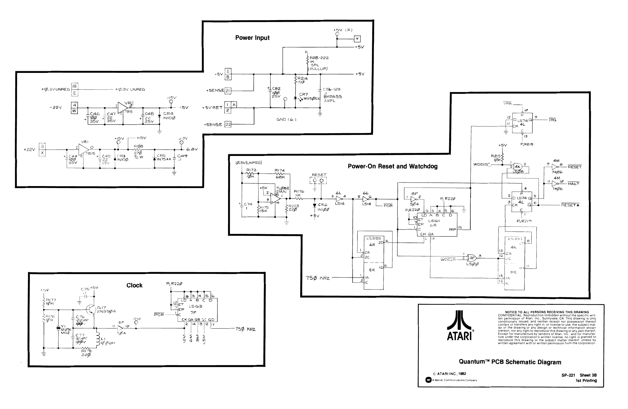
ey +19.3V UNREG — +1D.3V UNREG EJ -15V VR; IWS T isv 7p Tose cra INjIog
eV t e38v t Fe! \ 27 eas @7°'S | cas £o53. 5% crs lcae INIOD aa vl +22V EE] [e)
Power Input
+9OV (2)
R2i8-222 K SPL PULLUP)
R24 1s@
+SENSE[2) eee i aallaaal pe cR7 A 2a BYPASS if \wwvedsa} SXpL LIA +8VRET —
1B.3V(UNREG) GND (Ee)
Power-On Reset and Watchdog
4m woo1st RESET
RESET*
NOTICE TO ALL PERSONS RECEIVING THIS DRAWING CONFIDENTIAL: Reproduction forbidden without the specific writ ten permission of Atari, Inc., Sunnyvale, CA. This drawing is only conditionally ‘ssued, and neither receipt nor possession thereot
confers or transfers any right in, or license to use, the subject mat Except for manufacture by vendors of Atari, Inc., and for manufac
ter of the drawing or any design or technical information shown thereon. nor any righ\ to reproduce this drawing or any part thereot Except for manufacture by vendors of Atari, Inc., and for manufac. ture under the corporation's written license. no right is granted to reproduce this drawing or the subject matter thereof, unless by written agreement with or written permission from the corporation A
ATARI
© ATARI INC., 1962 SP-221 Sheet 3B + ware: Communcarions Company 1st Printing
This page is a drawing, shown as the original scan.
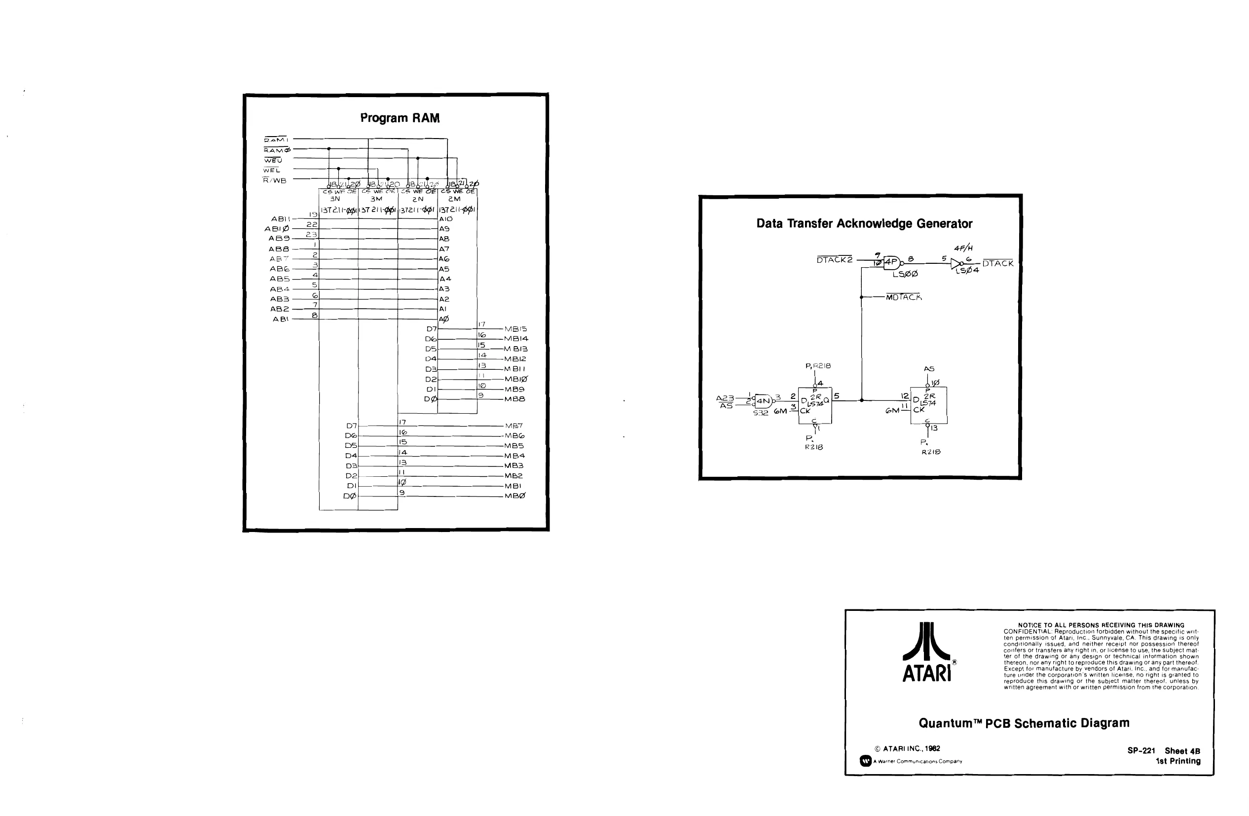
Program RAM
i delates ha ltes CS WE OF 3N
i3Te1 gp C2 we Cel cs We OF 3M 2n (37 21 1-Ppr 3721 - OPE 2m (3721-1 AIO AS AB AT AG AS AS o> [Jor for |p ts [ro | fu |v JG
IAS
AZ, AL Ap
Data Transfer Acknowledge Generator
4e/4 eZ DTACK2 —ygf4P pS ___* 55 DTACK LSB ce
—MDTACK,
NOTICE TO ALL PERSONS RECEIVING THIS DRAWING CONFIDENTIAL: Reproduction forbidden without the specific writ: ten permission of Atari, Inc., Sunnyvale, CA. This drawing is only conditionally issued, and neither receipt nor possession thereot confers or transters any right in, of license to use, the subject mat. ter of the drawing or any design or technical intormation shown
& thereon, nor any right to reproduce this drawing Or any part thereot
Except ior manufacture by vendors of Atari. Inc., and for manufac ture under the corporation's written license, no right is granted to reproduce this drawing or the subject matter thereof. unless by written agreement with or written permission from the corporation
© ATARI ING,, 1982 SP-221 Sheet 4B A wore: Communications Compary Ast Printing
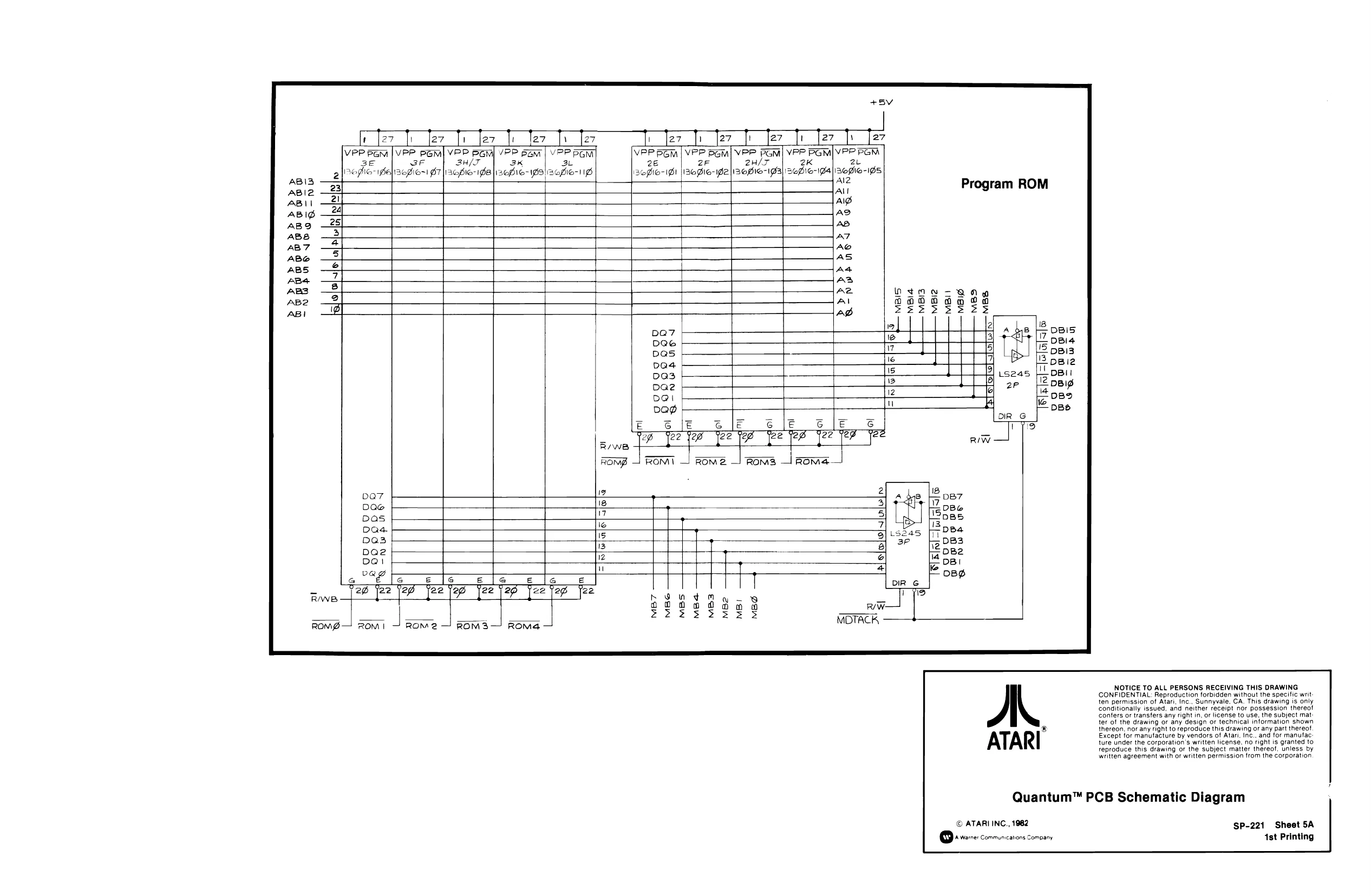
This page is a drawing, shown as the original scan.
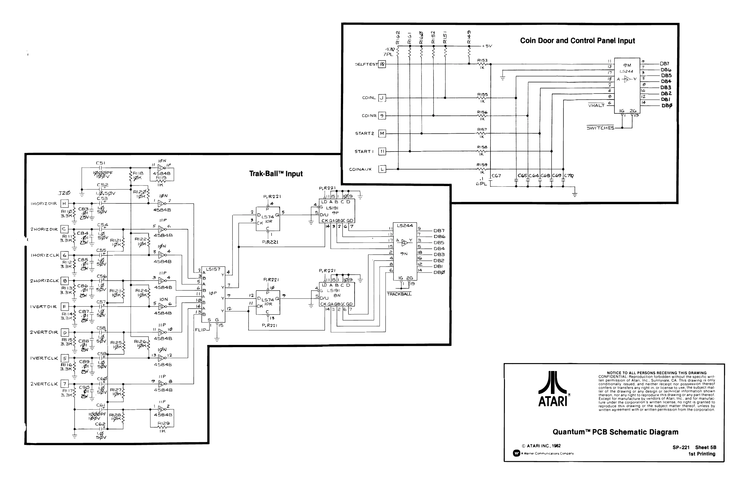
This page is a drawing, shown as the original scan.
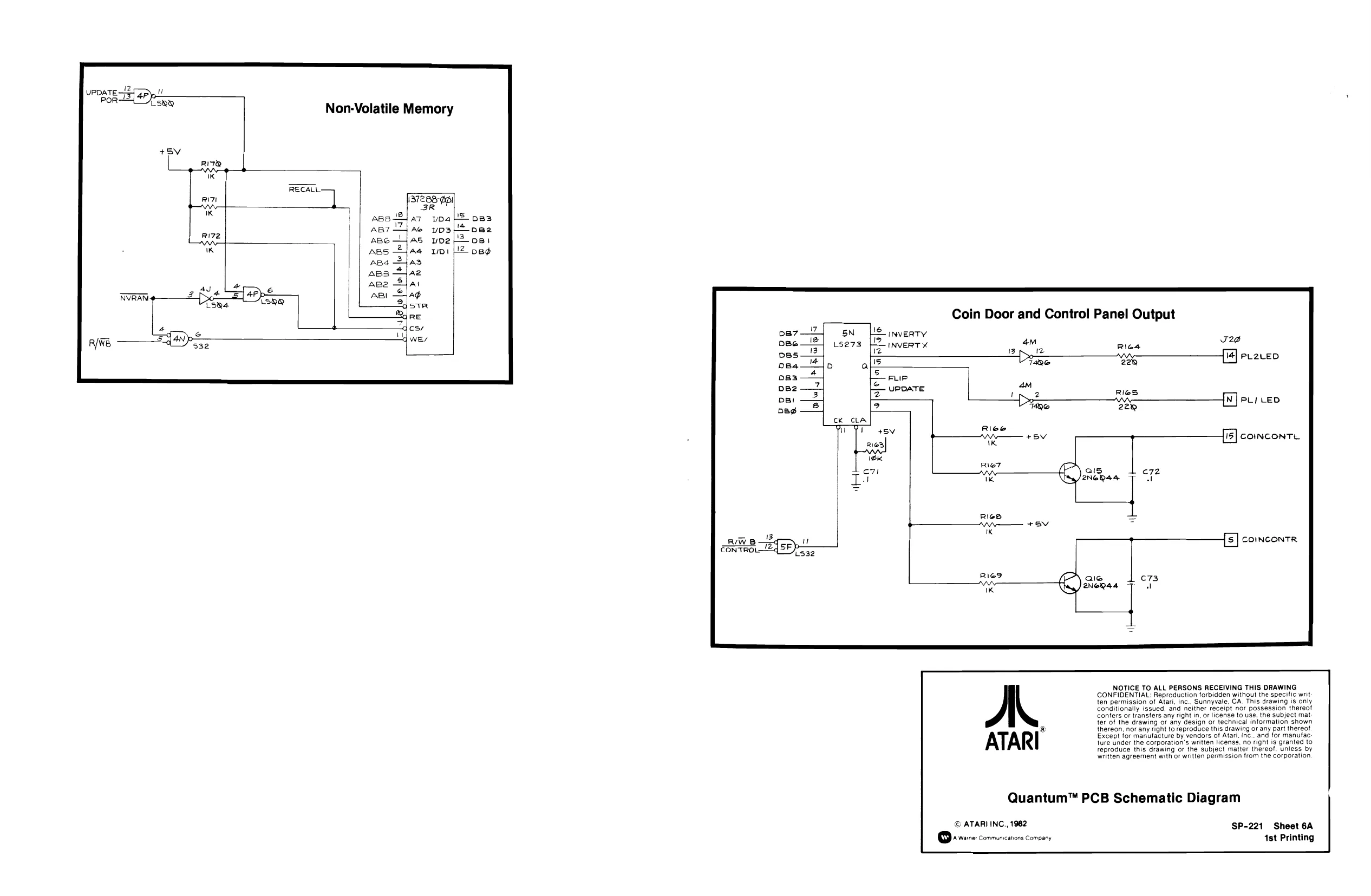
This page is a drawing, shown as the original scan.
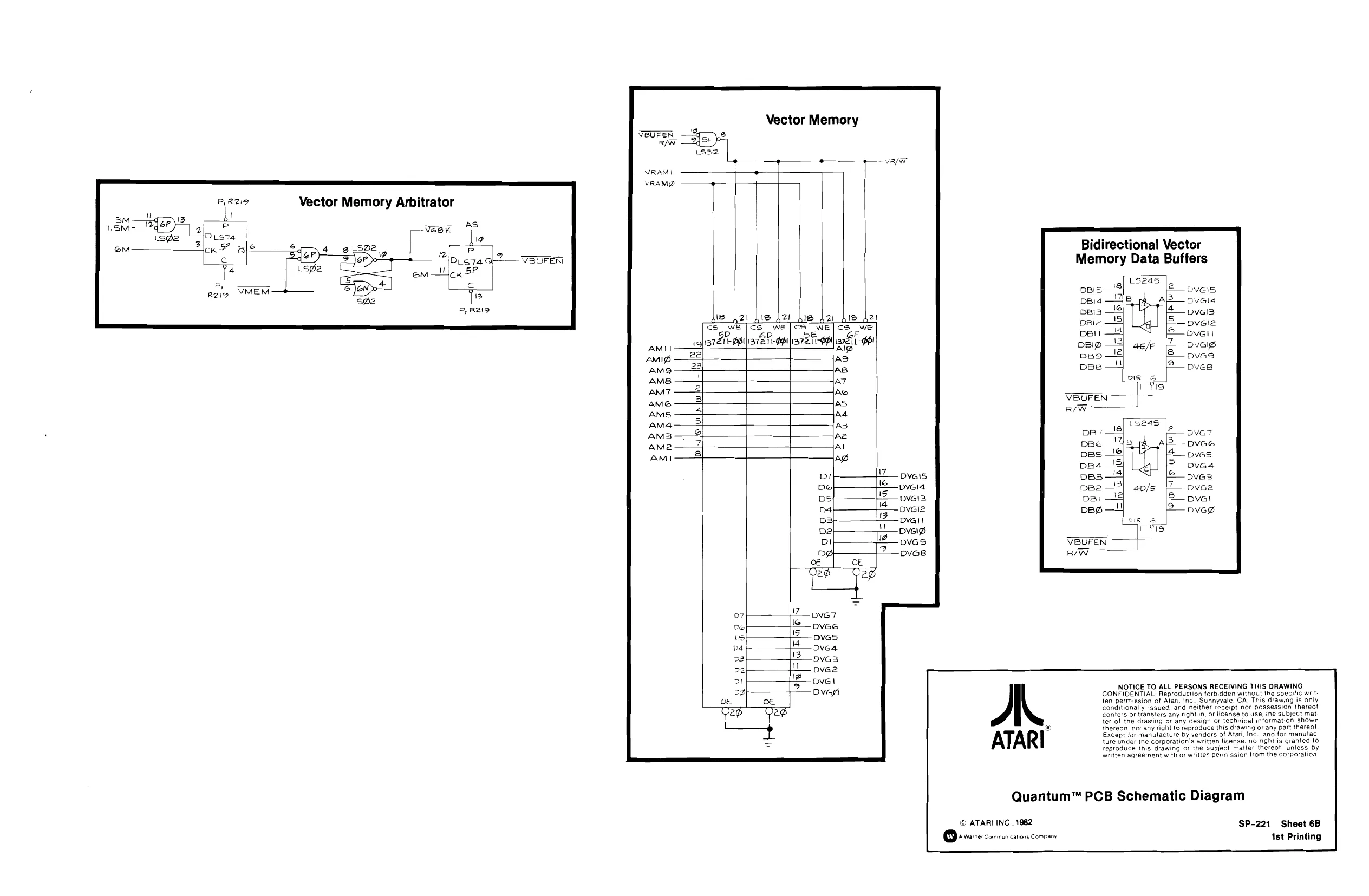
This page is a drawing, shown as the original scan.
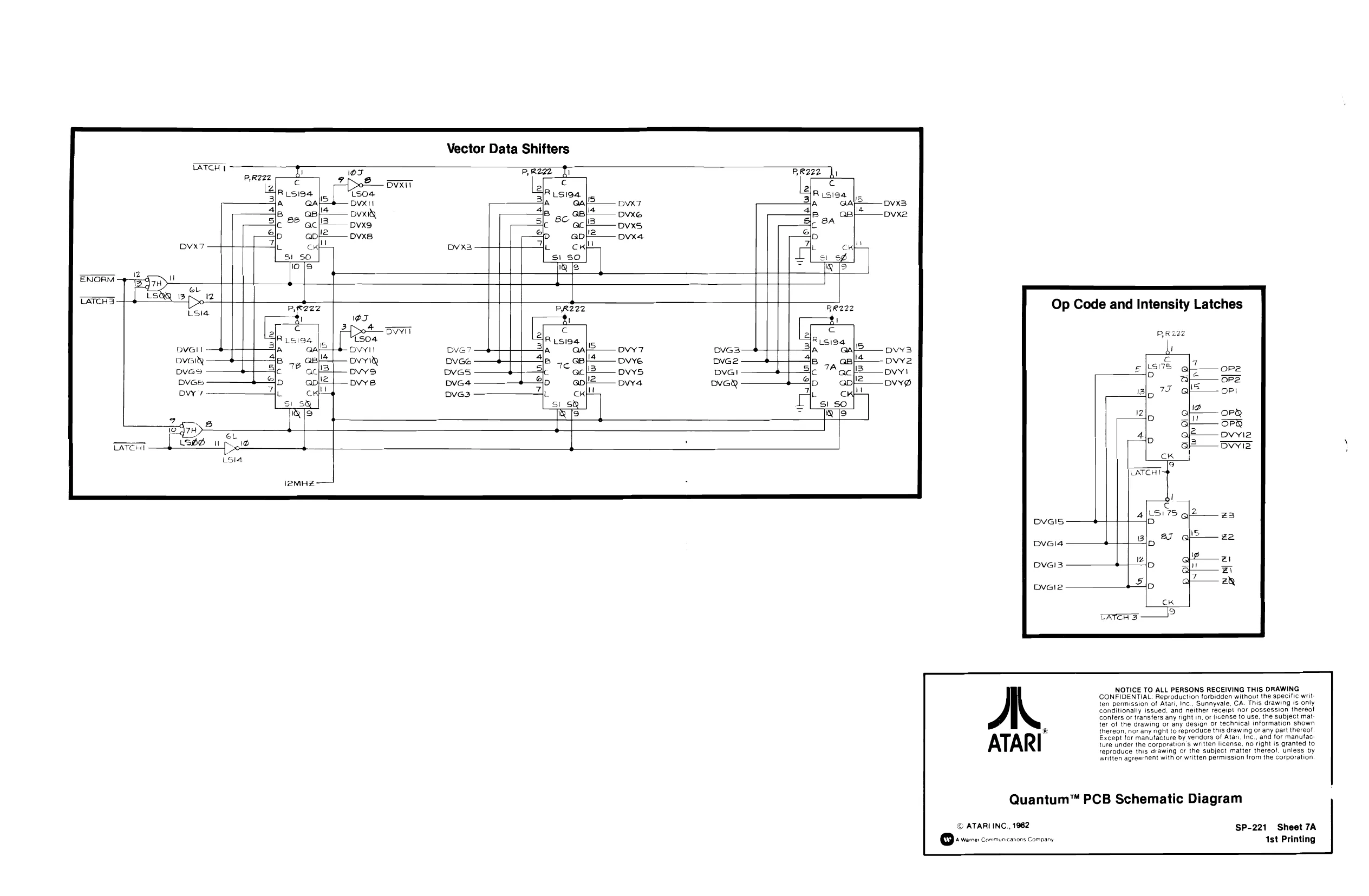
Vector Data Shifters
Pez _ fh ¢ Risisa iA al
aa) BC Ic
p aod
ENORM
TATCHS
Op Code and Intensity Latches
PK 222
pvGit DvGrty——+ pves DVGS
Dv? Doo
jaz 6L TATE (SdH f 1
Leia pp DIO wy
temHz-——
NOTICE TO ALL PERSONS RECEIVING THIS DRAWING CONFIDENTIAL: Reproduction forbidden without the specific writ ten permission of Alan, Inc, Sunnyvale, CA. This drawing is only conditionally issued, and neither receipt nor possession thereof Confers of transfers any right in, or license to use, the subject mat ter of the drawing or any design oF technical information shown a thereon. nor any right to reproduce this drawing or any part thereof. Except for manutacture by vendors of Atari, Inc., and for manutac: ture under the corporation's written license. no right is granted to reproduce this drawing or the subject matter thereo!, unless by written agreernent with or written permission from the corporation
© ATARI INC., 1962 SP-221 Sheet 7A Q > vercer Communicaons Company 1st Printing
This page is a drawing, shown as the original scan.
This page is a drawing, shown as the original scan.
This page is a drawing, shown as the original scan.
This page is a drawing, shown as the original scan.
This page is a drawing, shown as the original scan.
This page is a drawing, shown as the original scan.
This page is a drawing, shown as the original scan.
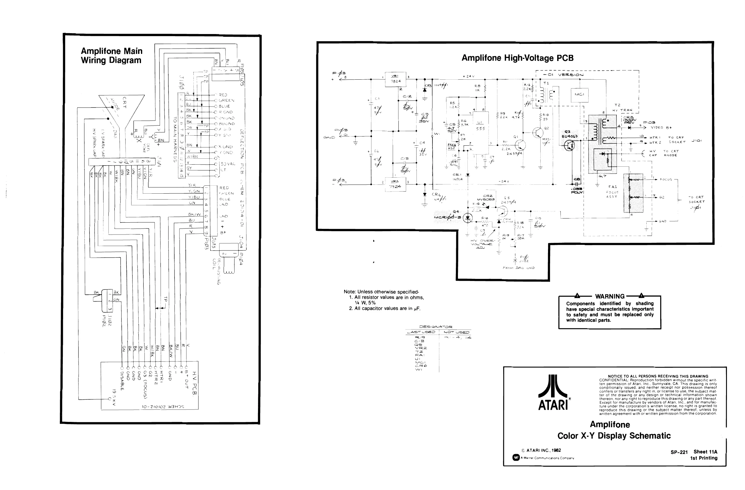
Amplifone Main Wiring Diagram
Amplifone High-Voltage PCB
GREEN jo SLUE
tO BUOND 0429 ae "BRY ccs J oS ico ee ' on er 4fo-yoe ree soener 7'O! nN Loy Sto cave —C (GND +O [Sovac WO 4Yve NH G3NYVH NIV OL
ay ro crt ANODE
- All resistor values are in ohms, % W, 5%
- All capacitor values are in uF.
as VRe +2 FA: un | Re Yan
29 © 2uLH« vate © revsia «snr04) €9° confers or transfers any right in, or license to use, the subject matter of the drawing or any design or technical information shown
thereon, nor any right to reproduce this drawing or any part thereof,
Except for manutacture by vendors of Atari, Inc.. and for manufac. jure under the corporation's written license. no right is granted to reproduce this drawing or the subject matter thereof, unless by written agreement with or written permission from the corporation NOTICE TO ALL PERSONS RECEIVING THIS DRAWING CONFIDENTIAL: Reproduction forbidden without the specific writ ten permission of Atari, Inc., Sunnyvale, CA, This drawing is only Conditionally issued, and neither receipt nor possession thereo!
®
lo- 210102 W3HIS
Amplifone
Color X-Y Display Schematic
© ATARI INC., 1982 SP-221 Sheet 11A 1st Printing
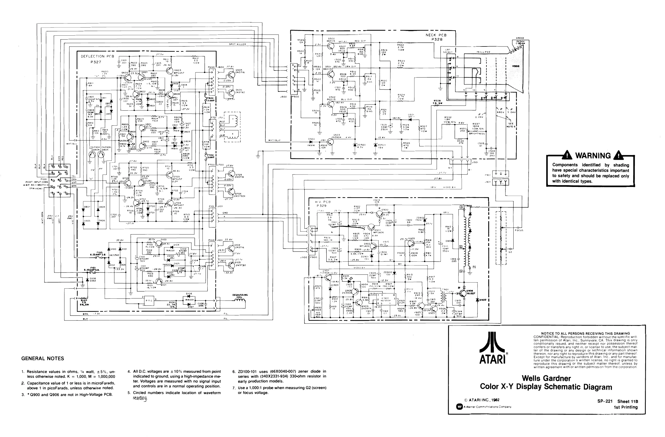
NECK PCB = 2328
DEFLECTION PCB rf — -
‘ f
| ie | 301 | Cort | |||
| ' | a | | | we | ae | | teow |
| | | ves | “TT | Fetts | 383 | - |
1 x Wem10% gey
tt
| H | soo | at | LL | -- | jie | - |
rot sc 529
| . | ¥ | yj | « | 25 rv |
8] asvler J Sheeran rn a
nn al ee aig \euzor -_ onscor SF fe sash Desc | Leos
at
GENERAL NOTES
- Resistance values in ohms, Ye watt, 5%, unless otherwise noted. K = 1,000, M = 1,000,000
- Capacitance value of 1 or less is in microFarads, above 1 in picoFarads, unless otherwise noted.
- *Q900 and Q906 are not in High-Voltage PCB. 4, AllD.C. voltages are + 10% measured from point indicated to ground, using a high-impedance meter. Voltages are measured with no signal input and controls are in a normal operating position.
- Circled numbers indicate location of wavetorm reading.
- ZD100-101 uses (66X0040-007) zener diode in series with (340X2331-934) 330-ohm resistor in early production models.
- Use a 1,000:1 probe when measuring G2 (screen) or focus voltage.
WARNING
Components identified by shading have special characteristics important to safety and should be replaced only with identical types.
A,
ATARI
NOTICE TO ALL PERSONS RECEIVING THIS DRAWING CONFIDENTIAL: Reproduction forbidden without the specific writ: ten permission of Atari, Inc., Sunnyvale, CA. This drawing is only Conditionally issued, and neither receipt nor possession thereof
conters or transfers any right in, or license to use. the subject mat
ter of the drawing or any design or technical information shown
thereon. nor any right to reproduce this drawing or any part thereo!
Except for manufacture by vendors of Atari. Inc., and for manutac ture under the corporation's written license. no right is granted to reproduce this drawing of the subject matter thereof, unless by written agreement with or written permission from the corporation
Wells Gardner
Color X-Y Display Schematic Diagram
© ATARI INC., 1982 SP-221 Sheet 11B 1st Printing