Reactor
Reactor (Gottlieb, 1982) · Manual · 44 pages · 71 sections · original scan
This page carries no recoverable text. It is a drawing or a photograph. See the original scan.
REACTOR #GV-100
INSTRUCTION MANUAL
ADDENDUM
- PAGE #8, LAST LINE UNDER VOLTAGE SHOULD READ:
MONITOR AND MARQUEE: 100VAC or 115VAC, 60HZ.
- PAGE #36, SERVICE PANEL ASSY.
| ITEM | DESCRIPTION | PART NO. |
| 1. | SERVICE PANEL ASSY. | MA=-300 |
| 2. | CABLE ASSY. | MA-316 |
| 3. | SWITCH (PUSH BUTTON) | EL-57 |
| 4. | SWITCH (TOGGLE) | EL-85 |
| 5. | VOLUME CONTROL | XO-104 |
| 6. | COIN METER | EL-84 |
REACTOR (GAME GV-100) INSTRUCTION MANUAL
SEC. PAGE
L INSTALLATION ...........00.00.0 0. cece 1
i. INITIALIZATION.............0..05..0. 0c 3
il. GAME OPERATION...........................000. 3
IV. GAME PLAY AND SCORING ...................... 4
V. SOUND/SPEECH ........0.00.0 0... 6
Vi. GAME ADJUSTMENTS/OPTIONS ................ 6
Vil. BOOKKEEPING AND SELF TEST ................. 7
Vill. GENERAL INFORMATION ........................ 8
1X = THEORY OF OPERATION......................... 9 xX WIRING AND SCHEMATIC DIAGRAMS .......... 11
Xi. PARTS INFORMATION ............................ 33
WELLS GARDNER MONITOR, SERVICE AND OPERATION MANUAL (Attached)
FOR SERVICE, CALL TOLL FREE: 800-323-9121; (ILLINOIS) 800-942-1620
I. INSTALLATION
MA2I6 ‘Ab SOUND/SPEECH ASSY,
A303 2345678 'A3 POWER SUPPLY f ae ° fai] MA-306
ASSY,
8.21976 MA298 A308 GAME ADJUSTMENT INTERFACE CABLE ‘LLUMINATION —SPEAKER/MARQUEE SWITCHES ASSY
ASS. ASS [PART OF AI LOGIC BOARD
A289 AI LOGIC BOARD ASS. MASTER ELECTRONICS PANEL,
‘ON/OFF SWITCH
REAR DOOR
“ Lock
TRACK BALL PLAYER SWITCHES
[TYPICAL
A300
SERVICE PANEL
ASS
FRONT DOOR
LOCKS
STEP/TEST SELECT TEST VOLUME COIN CABINET ae SWITCH SWITCH CONTROL METER
MA301 TRANSFORMER BRIDGE F2 BOTTOM PANEL, RECTIFIERS 63V.AC ASS, FUSE COINCHUTE §COINCHUTE COINCHUTE — FRONT DOOR #2 # INTERLOCK
AlaPEy Al
SERVICE
E CONN SWATCH #
POWER FUSE
A. 1. I. INSTALLATION
SET—UP Carefully inspect the exterior of the game for any damage which might have occurred during shipment.
. Remove the two screws from the back door, that were used for extra security during shipping.
. Unlock and open the rear cabinet door.
. Check that all plug in connectors are seated firmly. The connectors are keyed so they will only go in one way.
. Remove the binding strap from the line cord, and install the line cord plate in the groove provided (see photo).
. Adjust the cabinet levelers as necessary.
LINE CORD PLATE
CHECK-OUT . Check that all cables are free of moving parts.
- Check for any loose wires.
. Check for loose solder or foreign matter on switches and power supply assemblies.
. Be certain ail fuses are seated firmly.
. Be sure transformer wiring corresponds to the supply voltage.
Refer to section VI to make all the necessary game adjustments.
. _Reassemble the game.
. Plug the line cord into a properly grounded 3-wire receptacle ONLY! Cc CONTROL PANEL REMOVAL
2.
3: Unplug the game.
Unlock and open the coin chute door.
Reach in through the coin chute door and remove the wing nut and flat washer from each of the two carriage bolts which secure the control panel to the game. Remove the carriage bolts.
. Pull the control panel back, grasp it at the front edge as far back as it will go (approximately 14").
. Raise the front of the control panel approximately one inch above its supports and lift the entire assembly high enough to disconnect plugs AQJI/A9PI and A9J2/A9P2.
. Remove the entire control panel assembly from the game.
Track Ball assembly and leaf-switches are now accessible for removal or cleaning.
MONITOR REMOVAL . Unplug the game.
. Perform the contro! panel assembly removal procedure (Section C)}.
. Remove the outside shield, glass and monitor mask and put them aside in a secure place.
. Unlock and open the rear cabinet door.
. NOTE: The color monitor contains HIGH VOLTAGES delivering LETHAL quantities of energy. Do not attempt to service the monitor until you have shorted the anode plug on the picture tube to ground.
. Disconnect the video plug AI7JI, the monitor power supply plug Al2J3/A12P3 and the ground wire from the monitor chassis. From the rear of the game, remove the one unit and two washers from each of the four carriage bolts used to secure the monitor to the platform.
From the front of the game, remove the monitor, being careful to clear all cables from the CRT neck.
For reassembly, reverse the above procedure.
Hl. INITIALIZATION, lll. GAME OPERATION
Il. INITIALIZATION
TURN GAME ON Immediately, all of the illumination lamps turn on. These include the control panel lamps, the coin chute lamps and the speaker marquee lamp.
AFTER A TEN SECOND DELAY A. The attract mode appears on the screen.
B. The playing field cycles through the following:
- Gottlieb logo
- High Game to Date screen
- Game Play
DEPRESSING ANY CONTROL BUTTON The instruction set will now appear on the playing field and follow through game play and strategies.
lll. GAME OPERATION
A. GAME START
- Insert coins into coin chute. a. Coin chute tune is played. b. Total credits are displayed on screen.
- Press one or two player button to start game. (3 ships/25° or 7 ships/50°)
a. Instructions are displayed on screen. b. Total credits are decreased by one. c. Game initializes.
B. FIRST PLAYER
- The first player's score displays a zero.
- The other player's display will be blank.
- When the player loses his ship, any bonus earned is scored.
Cc. SECOND PLAYER
- Additional player is indicated by a zero in the second player's display.
D. EXTRA SHIPS/DECOYS
- Extra ships are earned (dependent on Switches #7 and #8) by achieving certain score levels.
- Extra decoys are earned by knocking down both sets of control rods.
IV. GAME PLAY AND SCORING
HOW TO PLAY
The game activity starts with the player's ship contained within the heart of a nuclear reactor. The player moves his ship using a track ball, and has the use of a rapid fire energy button and a decoy button to protect himself.
During the game play, the core expands as the enemy particles attempt to destroy the player's ship by deflecting it against the kill wall. Simultaneously, the player must destroy the enemy particles by using his ship to deflect them against the kill wall.
Pushing the energy button (located on the control panel) when the player's ship is in contact with an enemy particle, will increase the force applied to both the player's ship and enemy particle. When the decoy button is pushed, a decoy will emerge from the player's ship. The decoy will remain stationary at the point where the ship was located when the button was pushed. The decoy confuses the enemy so that they attack the decoy instead of the player. The decoy cannot be destroyed and should be placed in one of three positions:
- Next to a kill wall.
- In front of the control rods.
- Inside the entrance to the bonus chambers.
In doing so, the enemy particles will be lured into a Position which will allow the player to:
- Destroy them against a kill wall.
- Destroy the control rods.
- Trap them in the bonus chamber.
@ Knocking down either set of control rods, with enemy particles, will reduce the size of the core.
® Knocking down both sets of contro! rods will add an extra decoy. © After every 15,000 points, the player earns one extra ship. (Dependent on switches #7 and #8.}
While the enemy particles are in the bonus chambers, they will deflect off one another and the walls. As they are deflected off the walls, bonus is scored. To achieve maximum bonus, the player must use the ENERGY button to hold the enemy particles in the bonus chamber as long as possible.
The player earns 15 points per bounce during the early rounds and 15+ per bounce as the game progresses. On each round, point values per bounce increase.
As the play progresses, the reactor core continually grows in size, which decreases the usable playfield.
During the early rounds the core is a rectangular shape which expands outward forcing the player closer to the dangerous kill wails. The player can shrink the core by destroying either set of control rods, or killing the total amount of enemies “TO GO" for each round.
In later rounds the rectangular expanding core is replaced with an expanding and swirling vortex. Unlike the rectangular core, the vortex is deadly to the player. As it enlarges, it will draw the player to
its center and destroy him. A skillful player can get
out of the vortex even after it has caught him by moving his ship in a clockwise direction.
The ideal game play is a balance of using the decoys and bounce chambers to accumulate large bonus points, extra ships and using the control rods to gain extra decoys.
ROUND PROGRESSIONS
The following chart lists round progressions for Reactor:
Commencing with set three, the outer kill walls become invisible and remain that way for the rest of the game.
In set five and on (round 33), set four repeats itself, but the enemy particles gain more speed and mass, and are harder to kill. The control rods in each set, for the rest of the game will be nine.
IV. GAME PLAY AND SCORING
ROUND PROGRESSIONS CONTROL RODS ROUND] CORE | MAXIMUM ENEMIES ON SCREEN | “TO GO" | __IN EACH SET
| 1 | 3 Positrons | 3 |
2. 4 Positrons 3
| 3 | 5 Positrons | 5 | |||
| SETI | 4. | | Expander | 3 Positrons, | Nucieon | 5 | |
| 5. | | Expander | 2 Positrons, 2 Nucleons | 5 | ||
| 6. | | Expander | 3 Nucleons | 5 | ||
| 7. | | €xpander | 2 Positrons, | Lepton | 36 | 5 | |
| 8. | | Expander | 1 Lepton, | Nucleon | 40 | 5 | |
| 9. | | Vortex | 3 Positrons | 12 | 5 | |
| 10. | | Vortex | 4 Positrons. | 16 | 5 | |
| 11 | | Vortex | 5 Positrons | 20 | 5 | |
| SET2 | 12. | | Vortex | 3 Positrons, | Nucleon | 24 | 5 |
| 13. | | Vortex | 2 Positrons, 2 Nucleons | 32 | 5 | |
| 4 | | Vortex | 3 Nucleons | 36 | 5 | |
| 15, | | Vortex | 2 Positrons, | Lepton | 36 | 5 | |
| 16. | | Vortex | 1 Lepton, 1 Nucleon | 40 | 5 | |
| 17. | | Expander | 3 Pions | 2 | 7 | |
| 18. | | Expander | 4 Pions | 6 | 7 | |
| 19. | | Expander | 5 Pions | 20 | 7 | |
| SET3 | 20. | | Expander | 3 Pions, 1 Nucleon | 24 | 7 |
| 21. | | Expander | 2 Pions, 2 Nucleons | 32 | 7 | |
| 22. | | Expander | 3 Nucleons | 36 | ? | |
| 23. | | Expander | 2 Prons, I Lepton | 36 | 7 | |
| 24. | | Expander | 1 Lepton, 1 Nucleon | 40 | 72 | |
| r 25. | | Vortex | 3 Pions | 12 | 7 | |
| 26. | | Vortex | 4 Pions | 6 | 7 | |
| 27. | | Vortex | 5 Pions | 20 | 7 | |
| SET 4 | 28. | Vortex | 3 Pions, 1 Nucleon | 24 | 7 |
| 29. | Vortex | 2 Pions, 2 Nucleons | 32 | 7 | ||
| 30. | | Vortex | 3 Nucleons | 7 |
2 Pions, I Lepton 7 1 Lepton, 1 Nucleon 7
SCORING
UNUSED DECOYS PIONS BONUS CHAMBERS
© Score 500 points © Score 75 points Dependent on Switch #6
LEPTONS POSITRONS ON 15 or 15+ NUCLEONS PHOTONS
© Score 400 points ® Score 50 points OFF 10 or 10+ ® Scores 15 points (Rounds 1-4)
® Scores 16 points (Rounds 5-8) © Score 200 points @ Do not score. © Scores 17 points (Rounds 9-12)
NEUTRINOS CONTROL RODS © Scores 18 Points (Rounds 13-16) © Score 100 points Score 50 points © Scores XX + 1 point every 4 rounds, etc
© Score 100 points Score 50 points © Scores XX + 1 point every 4 rounds, etc.
CONTROL PANEL INSTRUCTIONS
RULES TACTICS Track Ball controls player movements. © Lure enemies close to outer wall for easier hits. Bounce enemies into outer wall to destroy them. e Player will be destroyed by touching outer wall. @ Completing one target bank shrinks core. © Completing both target banks wins one extra decoy. ® Knock enemy into bonus chamber for bonus points. Use ENERGY for more power to repel enemy. Use DECOY to distract enemy. e Place decoy by outer wall for easier hits. @ Place decoy inside bonus chamber for big bonus, and be carefull © Place decoy by target banks to earn more bonus and shrink core. Use early rounds to build up decoy reserves for later rounds. © TOGO indicates number of enemies left in round.
V. SOUND/SPEECH, VI. GAME ADJUSTMENTS /OPTIONS
V. SOUND/SPEECH
ATTRACT MODE
SPEECH OCCURRENCE
“WARNING CORE UNSTABLE” When core changes to vortex.
GAME MODE
“WARNING CORE UNSTABLE” ‘When core changes to vortex. “2000” After 2000 bonus is accumulated. “5000” After 5000 bonus is accumulated. “10,000” After 10,000 bonus is accumulated. “15,000-55,000" Every 5000 increment is spoken through 55,000 points.
“40 TO GO” When there are 40 enemy particles to go.
“32 TO GO” When there are 32 enemy particles to go.
“24 TO GO” When there are 24 enemy particles to go. ~
“16 TO GO” When there are 16 enemy particles to go.
“8 TO GO” When there are 8 enemy particles to go.
“ACTIVATE CHAMBER” When entering BONUS CHAMBER for the first time.
Vi. GAME ADJUSTMENTS/OPTIONS
A. CONTROL BOARD SWITCH ADJUSTMENT SWITCH 1 ____ INITIATED ATTRACT MODE ON. eee ee eee ees eee Sound and Instructions
| OFF | vive | + -Instructions/No Sound |
SWITCH 2 ATTRACT MODE ON OFF
SWITCH 3 ON... ».. Upright OFF + Cocktail
SWITCH 4 NORMAL/FREE ON... : Normal Game OFF +++. Free Play SWITCH 5 CREDITS/COINS VI OFF wiy2
SWITCH 6 BOUNCE CHAMBER
| ON, sixes | Pree | oer | eeterT Tt TeitT | ee | .. 15 Points |
OFFI 10 points
SWITCHES 735... PE SHIPS OFF OFF - Every 10,000 Points
| ON) | OFF | . Every 12,000 Points |
| ON | ON | . Every 15,000 Points |
| OFF | ON | -. Every 20,000 Points |
B. SOUND ADJUSTMENTS The audio output is controlled by the potentiometer mounted on the service panel assembly (located inside the coin mechanism door).
Turning the potentiometer counter-clockwise will decrease the volume. Turning it clockwise will increase the volume.
Cc. MONITOR ADJUSTMENTS Normally, few if any adjustments are required for proper monitor operation. However, after any major repairs to the monitor chassis refer to the attached monitor manual.
Vil. BOOKKEEPING AND SELF TEST
BOOKKEEPING
The bookkeeping functions of Reactor (GV-100) are limited to the electro-mechanical coin counter located inside the front door. Every time a coin is inserted into a coin slot, the counter is energized.
SELF TEST
The self-test consists of six functions which may be used to identify problems in the video system and to change program parameters. The self-test mode is entered by setting the self-test toggle switch located inside the cash door to “TEST”.
A selection of available tests is displayed on the
monitor. To return to the GAME mode at any time, the operator needs only to set the toggle switch back to “GAME”.
Selection of tests is done with the push button switch labeled “SELECT”. Upon entering the test
mode, a flashing arrow points to the first test
selection momentarily, depresssing the “SELECT” button will advance through each selection one by one. When the arrow is pointing to the desired test, the operator may begin that test by pressing the “SELECT” button and holding it down until the test appears on the screen.
Once a test has been selected, the operator can return to the selection list by holding down the select switch until it re-appears. The six tests are as follows:
- MONITOR ADJUSTMENT Four patterns can be displayed on the screen for adjusting monitor color, brightness, contrast and convergence. The patterns are: Color bars, a cross-hatch, a gray scale, and a dot pattern. By momentarily pressing the select switch, the operator may cycle through the four patterns.
- MEMORY For each RAM memory chip; a green check ( /} or red (x) appears signaling that the chip is good or bad respectively. For each ROM memory chip, a check sum is displayed. If you have a suspect ROM, refer to your distributor for the correct check sum number.
- SWITCHES/LAMPS A colored square is displayed for each player button. Pressing a button causes the appropriate square to change color. For each mechanism, a digit is displayed [initially 0). Inserting a coin into a coin chute will increment the appropriate value without affecting the coin meter.
Each player button contains a lamp. During this test, the lamps are turned on and off in various combinations. This happens independent of any button pressing or coin switch testing. When a lamp is lit, a picture of a light bulb appears on the screen under the appropriate colored square. By making sure the buttons are lit according to the light bulbs shown on the screen, this will determine whether or not the lamps are working properly. OBJECT PRIORITY Visual inspection must be used to determine the priority of two or more objects occupying the same area of the screen; that is, which objects appear to be in front of others and which are behind.
A total of 62 identical objects are placed on the
screen in 4 rows. Each object overlaps another such that the first object appears to be in front, and succeeding objects appear to be placed behind all previous ones. When this display is completed, the procedure is repeated such that each new object appears to be in front of all the previous ones. TRACK BALL This test allows the operator to align the track ball and check for slippage.
A figure which can be moved by the track ball is
placed on a grid. Movement of the figure is scaled down so that the track ball must be spun fairly rapidly to have the figure move an appreciable distance. The two digit number indicated on the left side of the screen is the absolute value of the difference between the horizontal and vertical distances moved. When the track ball is spun rapidly at a 45° angle, this number should be close to zero. DIP SWITCHES A functional description of the eight Dip Switches located on the Logic Board Assy. is displayed. Changing any switch will cause an immediate update of the description displayed on the screen.
Vill. GENERAL INFORMATION
A. PRINTED CIRCUIT BOARDS ARE DESIGNATED WIRE COLORS ARE SHOWN AS NUMBERS: AS FOLLOWS:
| Al | Logic Board Assy. | 0 Black | |
| A2_ | Interface Assy. | 1 Brown | 6 Blue |
| A3 | Power Supply Assy. | 2 Red | 7 Purple |
For example, 688 is a BLUE- SLATE-SLATE striped wire. Cc. FUSES
BOTTOM PANEL
| Fl | Primary Power | 4-Amp SLO-BLO |
F263 VAC 3-Amp SLO-BLO
| F3 | Monitor | 2 Amp SLO-BLO. |
POWER SUPPLY ASSY. (A3)
| FIT | +5VDC Source | 5 Amp SLO-BLO | |
| F21 | Sound/Speech Assy. | +30VDC | 1% Amp SLO-BLO |
| F31 | Sound/Speech Assy. | +12VDC | % Amp |
| F32 | Sound/Speech Assy. | -12VDC | ‘’% Amp |
| F41 | Coin Meter | +20VDC | 1 Amp SLO-BLO |
POWER SUPPLY SPECIFICATIONS
LOCATION
Logic Board Assy. Voltage adjustable. GAmps over-voltage Protection and fused for over-current protection. Sound/Speech Board 1.5Amps fused for over-current protection. The reference for this circuit is a IN5363 +30VDC Zener controlling the base of an emitter follower pass transistor.
Sound/Speech Board 100 milliamps fused for over-current protection. The plus and minus 12 volts supplies are the 7812 and 7912 IC regulators respectively.
Coin Meter Full wave rectified unfiltered voltage, fused for over-current protection.
Coin Chute Lights Full wave rectified unfiltered voltage, fused for over-current protection. Monitor and Marquee IOOVAC or MISVAC, GOHZ Isolated, fused AC voltage.
IX. THEORY OF OPERATION
INTRODUCTION The character based graphics system designated GG-Il has two main subdivisions. The first subdivision is the Central Processor Unit (CPU) which has three partitions: a. Microprocessors b. Memory Cc Input and Output ports (1/O}
The Intel 8088 microprocessor is used and 32K bytes of memory is reserved for programming space and has 5 input ports and 5 output ports. The second subdivision is the video state machine which generates and controls the video signal to the monitor. The state machine has three partitions: a. System Clock (CLK) b. Foreground generator (FGND) c Background generator (BGND)
The system clock is driven by a 20MHZ crystal, divided down for a 5MHZ dot clock.
All inputs and outputs including the video control and general purpose I/O are memory-mapped, (i.e. everything within the system can be addressed in a single segment of 64K addresses as memory).
The video control unit is divided into an “objectoriented” foreground driver and “character-oriented” background driver. The screen resolution is 256 pixels horizontally, and 240 lines vertically for both foreground and background. The CPU communicates with the foreground driver and background driver by writing data into the designated memory areas in a certain format The foreground is designed to display moving objects on the screen with a minimum overhead to the processor. The game programs will only have to specify the vertical and horizontal position and the object select number to the foreground driver. The background video supplements the foreground with relatively static figures on the screen. The CPU specifies all the character positions on the screen with desired “character ” patterns.
A 5MHZ system clock drives a 9 bit horizontal dot
counter and an 8 bit vertical line counter. The
horizontal counter counts from 0 to 255 during active scan line and 256 to 317 during horizontal blanking time. When the horizontal counter reaches 317, the horizontal counter resets to 0. At the beginning of the horizontal blanking time (horizontal counter = 256) it increments the vertical counter. The vertical counter counts from 0 to 239 during active vertical scan time and 240 to 255 during vertical blanking time.
SERVICE NOTES
X. WIRING AND SCHEMATIC DIAGRAMS, PARTS LISTS
TABLE OF CONTENTS
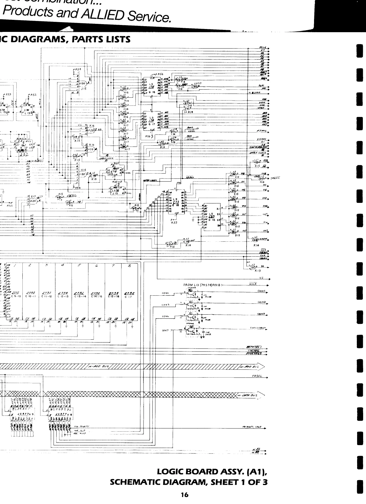
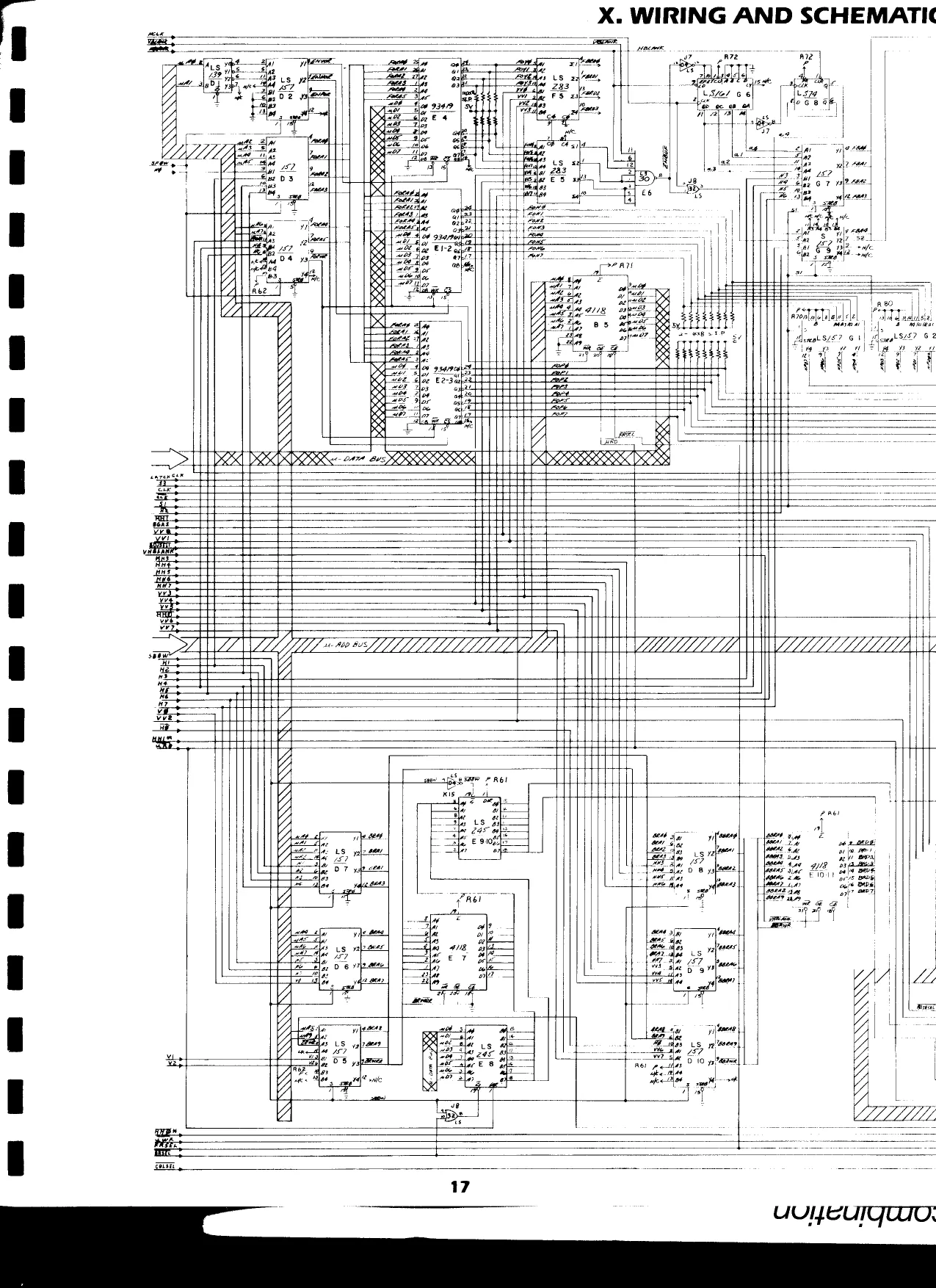
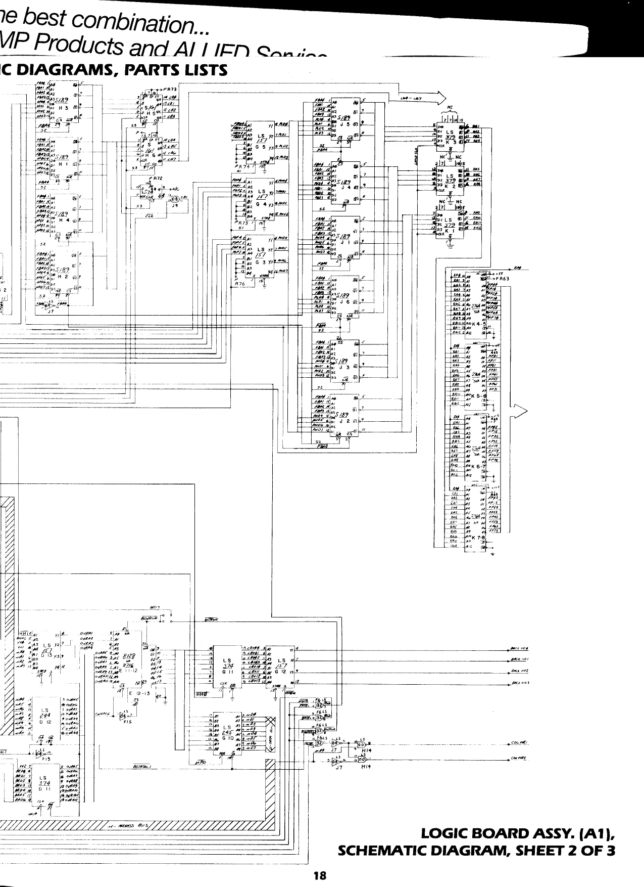
LOGIC BOARD ASSY. (A1) COMPONENT LOCATION AND PARTS LIST . . SCHEMATIC DIAGRAM (SHEET 1 OF 3) .. 15 SCHEMATIC DIAGRAM [SHEET 2 OF 3) .. 17 SCHEMATIC DIAGRAM (SHEET 3 OF 3) 19
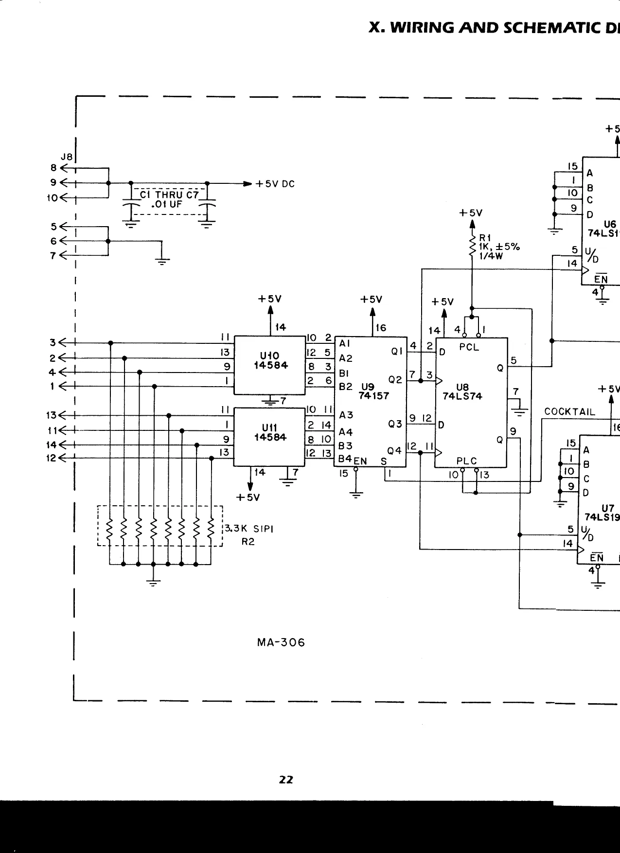
INTERFACE ASSY. (A2) COMPONENT LOCATION AND PARTS LIST 21 SCHEMATIC DIAGRAM
POWER SUPPLY ASSY. (A3) COMPONENT LOCATION AND PARTS LIST ... . SCHEMATIC DIAGRAM
SOUND/SPEECH ASSY. (AG) COMPONENT LOCATION AND PARTS LIST .... SCHEMATIC DIAGRAM
PRIMARY POWER/INTERCONNECTION DIAGRAM
X. WIRING AND SCHEMATIC DIAGRAMS, PARTS LISTS
REFERENCE
Al A2 A3
AB, A9, AIO BI B3 B4
88, B9, BIO Bi, B12 Bis c3 a ay ce C7, CB-9 9-10 10-11 cn2 C1213
14-15, 15-16 cr ol D2, DS, D6,D7. D8, D9, DIO, DIZ 03, D4 on oz O15
O17
EI-2, £2-3, £4 —S £6 &7 £8, E9-10 E10-11 EN-2 E13 E15
E16
FS Fo FS FIG
FIZ
LOGIC BOARD ASSY. (A1), PARTS LIST
DESCRIPTION
Logic Board Assy. 8284A Clock Driver 74LS02 Quad 2-input “NOR” gate 74LSI61 Synchronous Presettabie binary counter 7418377 Octal “D" Flip flop 8088 CPU 74LS374 Octal D-type flip flop 7415367 Hex 3-state buffer Expansion 7415138 | of 8 Decoder/Demultiptier 74LS139 Dual 1 of 4 decoder 74LS138 1 of 8 decoder 741240 Octal Buffer/line driver 741$240 Octal Buffer/line driver 7418374 Octal D-type flip flop 74LS245 Octal Bus transceiver 8128 (RAM 0} 8128 (RAM I} Expansion ROM 7 (2732A} 4K ROM 6 (2732A)} 4K ROM 5 (2732A) 4K ROM 4 (2732A) 4K ROM 3 (2732A} 4K ROM 2 (2732A} 4K ROM 1 (2732A] 4K ROM 0 (2732A} 4K 74LS13 9 ~ 8 EPROM 8 EPROM ~ 8 EPROM > 8 EPROM 8 EPROM 8 EPROM » 8 EPROM » 8 EPROM
7418157 Quad 2-input multiplexer 74157 Quad 2-input multiplexer 741$374 Octal D-type fiip flop 741$244 Octal Buffer/line Driver 741886 Quad 2-input exclusive- “OR” gate 7418283 4-bit binary full adder 74Si61 Synchronous presettable binary counter 93419 64 - 9 bipolar RAM. 7ALS283 4-bit binary full adder 741S30 8-input “NAND” 4118 IK 8 RAM 7415245 Octal Bus transceiver 4118 IK» 8 RAM 8128 (BGO) Static RAM 2K - 8 8128 (BGI) Static RAM 2K - 8 74LS86 Quad 2-input exclusive- “OR” gate 7418273. 8-bit register 741S20 Dual 4-input “NAND” gate 7415283 4-bit binary full adder 74132 Quad 2-input “OR” gate 74LS04 Hex inverter 748161 Synchronous presettable binary counter 741586 Quad 2-input exclusive “OR” gate DESCRIPTION
Gl, G2, G3, G4, G5 7415157 Quad 2-input multiplexer INTEGRATED CIRCUITS
PART NO. REFERENCE
MA-289 xO-478 G7 XO-428 cs XO-440 fer xO-97 xO-490 G9 xO-9 Gio xO-444 Gi G2 XO-437 GIB, Gi4, GIS XO-419 GI6, GI7 xO-437 HI, 2, H3, H4 XO-91 H5, H6, xO-91 xO-96 H7, H8, H9, HIO XO-79 Hin XO-486 HI2 XO-486 HI3 HI4 xO-485, His XO-485 Hi6, HI7 XO-485 XO-485 Ji, 32, 33, J4, J5, J6 XO-485 a7 XO-485 5. xO-485, jo XO-485 S10, J xO-419 Jz xO-390 4 xOnG JS XO-96 6, 517 XO-N7 XO-435 KI, K2, K3 Ka-5 xO-95, K5-6 XO-488 Ko-7
xO-99 K9, KIO, KI xO-95 Ki2 XO-432 KB XO-487 Kia xO-79 KIS xO-487 KI6 XO-486 KI7 XO-486 XO-435 14-5, 5-6 16-7, 17-8 XO-94 un XO-430 u2 XO-95, xO-433 u3 XO-418 XO-488 L314
XO-435 74157 Quad 2-input multiplexer 74LS74 Dual D-type Pos. edge trig. flip flop 74LSI61 Sync. presettable binary counter 748157 Quad 2-input multiplexer 7415245 Octal bus transceiver 741S374 Octal D-type flip flop 7415157 Quad 2-input multiplexer 7489 64-bit RAM 741174 Hex D flip flop 745189. 64-bit RAM 745161 Synchronous presettable binary counter 7418157 Quad 2-input multiplexer 7418260 Dual 5-input “NOR” gate 7418298 Quad 2-port register 7418157 Quad 2-input multiplexer 74100 Quad 2-input “NAND™ gate 741$30 8 input “NAND” gate 741S86 Dual 2-input exclusive “OR” gate 748189 64-bit RAM 741804 Hex inverter 741832 Quad 2-input “OR” gate 7408 Quad 2-input “AND” gate 93422 256 - 2 bipolar RAM 741802 Quad 2-input “NOR” gate 741874 Dual D-type flip flop 7407 Hex buffer/driver 741$30 8 input “NAND™ gate 748161 Synchronous presettable binary counter 7418379 Quad parallel register FGO 2732A 4K - 8 EPROM FG! 2732A 4K - 8 EPROM FG2 2732A 4K - 8 EPROM FG3_2732A 4K - 8 EPROM 7415157 Quad 2-input multiplexer 741S260 Dual 5-input “NOR” gate
74(S32 Quad 2-input “OR” gate
741808 Quad 2-input “AND” gate 741504 Hex inverter 741520 Dual 4-input "NAND™ gate 748161 Synchronous presettable binary counter
7418166 8-bit shift register 74LS20 Dual 4-input “NAND" gate 7ALSI61 Synchronous presettable binary counter 74574 Dual D-type pos. edge trig. flip flop 74804 Hex inverter PART NO.
xO-390 xXO-N14 XO-431
xO-440
XO-124 xXO-79 XO-% xO-390 XO-88 XO-442 xO-89 XxO-488
xO-390 XO-93 xO-118 XO-390 XO-427 XO-432 XO-435
xO-89 xXO-418 XO-433 xO-404 XO-100 xO-428 XO-434 XO-126 xXO-432 xO-488
xO-98 XO-485 XO-485 XO-485 xO-485 xO-390 xO-93 xXO-433 XO-86 xO-418 xO-430 XO-488,
xO-391 xO-430 xO-440
xO-87
xO-400
X. WIRING AND SCHEMATI
LOGIC BOARD ASSY. [A1},
MISCELLANEOUS ELECTRONIC COMPONENTS
| | | REFERENCE | DESCRIPTION | PART |
NO.
| CHH6 | Capacitor, 0.1 UF SOVAX.CR. | XO-230 |
*80%-20%
| | | C28 | Capacitor, 10 UF 25V AX. TANT. XO-127 |
10%
| C31-C34 | Capacitor, 0.1 UF AX CR. | XO-230 |
*B0%-20% 83
| cs | Capacitor, 100 PF 100V DIS. CR. | XO-128 |
| i | 10% | x} |
52 Capacitor, 0.1 UF 100V DIS. CR XO-626
| 10% | 5 | a4 |
ALL UNMARKED
| a | CAPACITORS | 01 UF SOV AX CR. *80%-20% | —XO-229 | . | — |
ALL POLARIZED i UNMARKED
| CAPACITORS | 10 UF 25V AX. TANT. 10% | XO-127 | | | ||
| DI, D8I | Diode, IN4148 | XO-261 | |||
| ar-a4 | Transistor, 2NG044 | XO-120 | I | ||
| Q8i-087 | Transistor, MPSA70 | XO-309 | 5 | 86 | | |
| RI, RIG | Resistor, 470 OHM, 5% “WW | XO-35, | (op | ce RAMI | |
| R31, R34 | Resistor, IK OHM, 5% WW | xO-5 | ~ | ——-} | —s |
| Ral, R42 | Resistor, S10 OHM, 5% “WW | XO-25* | oo | ||
| R43 | Resistor, 3.3K OHM, 5% %\W | XO-38 | a? | ||
| R44, RAS | Resistor, IK OHM, 5% 4W | xO-5 | bo | paw 2 | |
| R51, R52 | Resistor, 330 OHM, 5% ‘AWW | XO-34 | neaentienitoen | ||
| | | R53, R56 | Resistor, IK OHM, 5% YW” | xO-5 | ||
| R57, RSB | Resistor, 560 OHM, 5% “WW | XO-36 | |||
| R59-R62 | Resistor, IK OHM, 5% 4” | xO-5 | |||
| R6I-R71 | Resistor, IK OHM, 5% YW | XO-5 | |||
| R73, R74 | Resistor, IK OHM, 5% W | XO-5 | |||
| i | R76-R80 | Resistor, 1K OHM, 5% YAW | xO-5 | ||
| Rel | Resistor, 820 OHM, 5% VW | XO-174 | |||
| R82 | Resistor, 100 OHM, 5% AW | XO-28 | |||
| R83, R84 | Resistor, 15 OHM, 5% YW | xO-171 |
RBS Resistor, 180 OHM, 5% WW — XO-24
| R86, RB7 | Resistor, 15 OHM, 5% YW | xO-171 |
| R88 | Resistor, 180 OHM, 5% AW | XO-24 |
| R89, RIO | Resistor, 15 OHM, 5% Y4\X/ | xO-171 |
| Ra | Resistor, 180 OHM, 5% “AW — XO-24 | - |
| R92 | Resistor, IK OHM, 5% YW | XO-5 |
| R93 | Resistor, 2K OHM, 5% ‘4W | XxO-14 |
R94 Resistor, IK OHM, 5% Ya xO-5
| R95 | Resistor, 470 OHM, 5% V4” | XO-35 |
RIG Resistor, 240 OHM, 5% '4W/ — XO-173
| R97 | Resistor, 2K OHM, 5% “WW | XO-14 | } | ||
| ROB | Resistor, IK OHM, 5% YAW | xO-5 | ss | | | i |
| R99 | Resistor, 470 OHM, 5% “WW | XO-35 | i | ||
| R100 | Resistor, 240 OHM, 5% “WW | XO-173 | ipa] | |) Cie =13 ROMA | |
| RIO} | Resistor, 2k OHM, 5% WW | XO-I4 | | | | | |
| RIO2 | Resistor, IK OHM, 5% Y4\/ | XxO-5 | B13 | =——— | |
| R103 | Resistor, 470 OHM, 5% V4 | XO-35 | | | 7 | |
| R104 | Resistor, 240 OHM, 5% V4 | XO-173 | —-—- te | nt |
SiP 1, SIP 2 ci3-14ROMS SiP 71, SIP 72 i 1
| | | SIP 73 | Resistor, Dip, IK, 9 Pin | XO-493 | Bl4 | i | ; |
| sip 4 | Resistor, Dip, 4.7K, 9 Pin | XO-492 | eee | + | ||
| X-TALI | Crystal, 15 MHZ | ee | (ee | = | me | |
| XTAL 51 | Crystal, 20 MHZ | xO-494 | *% louf 25V aX. | | | |p cl4- 15 Rome! | |
| Dip Switch | XO-505 | TANT. | £20% | B15 | fo |
20 Pin Socket XO-491
| 22 Pin Dip Socket | XO-467 | 4-0 | Bow Aen} | —— | ||
| 24 Pin Dip Socket | XxO-529 | + 80% -20% | i | | | Seis roms | | |
| 28 Pin Dip Cocket | XO-536 | | | | |
i 40 Pin Dip Socket XO-530
cI? ROMO
B g ~
I) “a a “ ‘< < a u g UO g Q 9)
Q s g k Ww § = fe) U < > a <q Q < fe) IAT NCATE
ucts and AL
ca
D10
REP
X. WIRING AND SCHEMATI
fq aed 2:5, ez,
Ga BATA Bus)
SOCKET 9 wf
RENETWOKK
a: -
NTT.
- SE SIIMES AIT TY Pue sjonpalg ““UONPCUIQUIOD 189
This page is a drawing, shown as the original scan.
This page is a drawing, shown as the original scan.
This page is a drawing, shown as the original scan.
This page reads as a drawing: its text was drawn rather than typeset, and comes out in fragments. See the original scan.
IC DIAGRAMS, PARTS LISTS
an ify cet wee Bis eles Lg yp cen _| ma 57 Fast sion 13 rf Seae fatS ols 7 a ae a RS
eal it Ree | Re! | jar NOs | tee a oe oa he | 1 Abs MPSATD ee
__ Age | eh sah OF | ' | i meine aatars iil | | il i i| J { 130 if 1 ABs
LOGIC BOARD ASSY. (A1),
SCHEMATIC DIAGRAM, SHEET 3 OF 3
X. WIRING AND SCHEMATIC DIAGRAMS, PARTS LISTS
INTERFACE ASSY. (A2), COMPONENT LOCATION
INTERFACE ASSY. (A2); PARTS LIST
| > | REFERENCE | DESCRIPTION | PART NO. |
Interface Board Assy. MA-306
| cc7 | Capacitor, OIUF, SOV | XO-229 |
| RI | Resistor, 1K OHM, 5% YAW | XO-5 |
R2 Resistor, DIP, 3.3K OHM, 9PIN — XO-157
| U2, U3 | IC, SN74LS244, Octal Buffer | XO-N7 |
| U4-U7 | IC, SN74LSI91, Binary Counter | XO-N6 |
us IC, SN74LS74N, Dual-Flip Flop xO-434
| u9 | IC, SN74152, 2-1 Multiplexer | xO-114 |
| ui, Un | IC, 14584, CMOS Inverter | XO-N9 |
20 PIN Socket xO-491
This page is a drawing, shown as the original scan.
ATIC DIAGRAMS, PARTS LISTS
uz
i<s9
- u2 —~<5 T4LS244 yg —1-< 3
| AS | Y7 | Hy | i<16 |
| A6 | Ys | <18 |
AT f ‘
| A8& | 7 | | | |
| er | e2 | J | i |
| f | 19 | - | ; |
L<a7 ! i)
a = TRACKBALL - CLEAR eg OK TAIL, —t< 4 16 ‘
| 3 | YI | ' |
| 2 | v2 | \ |
| 6 | Y3 | t |
z 14
t
' +5V oem gS 20 4 el “ ' I ” fl
fRu
INTERFACE ASSY. {A2), SCHEMATIC DIAGRAM
X. WIRING AND SCHEMATIC DIAGRAMS, PARTS LISTS
POWER SUPPLY ASSY. (A3), COMPONENT LOCATION
D43
-voc®
ALL RIGHTS RESERVED
D.GOTTLIEB & CO
REFERENCE
CM, C32, C42 a2 13, C23 C14, C33, C43 C21, C22 C31, C4 DM, 025 035, D43
Diz
D2r-D24
031-D34, D36 D41, D42, D44 Fl Fai 31, F32 Fal Pl 4h ust ar
dk 32 33 4h D35 tu
D25 30 voc = R31
POWER SUPPLY ASSY. (A3), PARTS LIST
DESCRIPTION
Power Supply Assy Capacitor, .O1UF, 16V Capacitor, 100UF, 16V Capacitor, O.1UF, 100V Capacitor, 0.2UF, 16V Capacitor, 2200UF, 75V Capacitor, 470UF, 35V
Diode, Light Emitting MV-5752 Diode, Zener, 5.6V, 5%, IW, IN4 734A Diode. 1N5S401 Diode. Zener, 30V, 5%, 5W, 1N5363B
Diode, IN4004 Fuse, 614 AMP SLO-BLO Fuse, 1.5 AMP SLO-BLO Fuse, '@ AMP SLO-BLO. Fuse, | AMP SLO-BLO Connector, 4 PIN PART NO.
MA-303 XO-278 xO-235 xXO-234 xXO-205 XO-132 XO-284
xO-270
XO-255
XO-263 XO-273
xO-254 ELS £L-34 ELS EL6 PS-87, REFERENCE
p2 P3 Pe an ai Q21 Rit RI2 R13, RIF RIS RIG RZ RIB R21, R22 R23 R3I, R41 ScRII un U3 ut vRI DESCRIPTION
Connector, 10 PIN Connector, 7 PIN Connector, 16 PIN Transistor, PNP, 2N5879 Transistor, NPN, TIP3IB Transistor, NPN, 2N3055 Resistor, 470 OHM, 5% YAW Resistor, 100 OHM, 5% IW Resistor, 12 OHM, 5% 2W Resistor, 200 OHM, 5% “AW Resistor, 180 OHM, 5% YW Resistor, 100 OHM, 5% \X/ Resistor, 20 OHM, 5% YA\W/ Resistor, LBKOHM, 5% 2W Resistor, 200 OHM, 5% 5W Resistor, 750 OHM, 5% TW/ Silicon Controlied Rectifier Diode, Programmable Zener T1431 Voltage Regulator :12V, LM 340T Voltage Regulator -I2V, LM 320 Potentiometer, 100 OHM PART NO.
XO-531 XO-526 XO-372 XO-323 XO-641 XO-301 XO-55 xXO-137 XO-138 XO-143 xXO-24 XO-28 xXO-29 XO-135 xO-133 XO-136 xXO-131 xO-272 XO-473 xO-130 XO-134
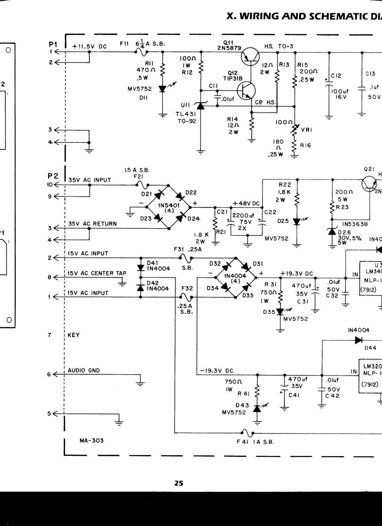
This page is a drawing, shown as the original scan.
; DIAGRAMS, PARTS LISTS
P4 +5V DC ( SOURCE) > 16
| IN4734A | +> | 15 |
loon 13 SCR II McRSa=|-e>® B.6V, 5% "3
| wut | iw | Hl |
50V rat H 20n ”
| 250 | rT | 10 |
4 ['* RIS >9 i + = KEY, 14
21 7 HS. TO-3
2N3 055 23 5
wluf 4 50V
IN4004 2
| P3 re | H +30V DC (SOURCE) >6
+12v Dc (SOUR i (SOURCE) 1s 4
t
7 abe i = |
KEY; 2 i i t —12v oc (source)! .2uf t > 16Vv ' C43 ‘
ALL RESISTORS ARE +5% !
i H +20v Dc 4
POWER SUPPLY ASSY. (A3), SCHEMATIC DIAGRAM
X. WIRING AND SCHEMATIC DIAGRAMS, PARTS LISTS
SOUND/SPEECH ASSY. (AG), COMPONENT LOCATION
jear yI 3.879545 MHZ R16 C45 P/0 AGPI
ca7
CLOCK Li
YI 3.579545 N
COPYRIGHT 1981 ALL RIGHTS RESERVED
SOUND/SPEECH ASSY. (AG), PARTS LIST
PART PART
REFERENCE DESCRIPTION NUMBER REFERENCE DESCRIPTION NUMBER NOTES:
1.UNLESS ¢
| Sound/Speech Assembly | MA-216 | RIS, R16 | Potentiometer. 10K ohm | XO- 109 | RESISTOR | |
| c1c2 | Capacitor, 0. 1UF, 25V | XO-248 | R18, R21 | Resistor, 100K ohm, 5%, ‘AW | xO45 | 2. TL LEGE |
| C4, CIB | R22 | Resistor, 2K ohm, 5%, | A\W/ | XO- 14 | INDICAT! | |
| C15, C16,C19 | R31 | Resistor, 68K ohm, 5%, WW = XO-189 | 3. WITH THI | |||
| €20, C21, C23 | RP 1, RP2 | Resistor, Dip | XO- 168 | E1,E2,€: | ||
| C25, C26 | SBI | Switch, Dip | XO-505 | SoLip’ Si | ||
| C28-C30, C33 | swt | Switch, Momentary Pushbutton = XO-5 15, | 2716 PRE | |||
| C42, C44 | ul | IC, 7414 | xO-397 | USED WI | ||
| 3 1-C32 | Capacitor, 047UF, 25V | XO-222 | u2 | IC, SN74LS74N | xXO-434 | Pfo AGRI |
| 37 | Capacitor, 4.7UF, 35V | xO-291 | U3 | CPU, R6502- 13, | XO-360 | |
| C3, C38-C41 | Capacitor, 47UF, 50V | XO-210 | U4 | IC, SN74LS 138N | XO-437 | |
| C14, C24 | Capacitor, 100PF | XO-223 | US, U6 | EPROM, 2716 | PR-53 | |
| C22 | Capacitor, 300PF | XO-283 | U7-U9, U1, UIB IC, SN74L875 | XO-394 | ||
| 27 | Capacitor, IUF, 50V | XO-217 | Ut0 | IC, SN74LS02N | xO-428 | |
| C36 | Capacitor, 470UF, 35V | XO-284 | ul2 | IC, SN7407N | XO-384 | |
| C45, C46 | Capacitor, 33°F | XO-277 | uB | IC, Inverter, SN74LSO5N | XO-411 | |
| c4a7 | Capacitor, .01 UF, 100V | XO-202 | um | Voice Chip, SCO1 | XO468 | |
| CRI | Diode, IN4 148 | XO-26 1 | UIs | RRIOT, R6532- 18 | XO-361 | |
| CR2 | Diode, Zener, 1N52258 | XO-269 | U6 | IC, SN74LS04N | xXO-4 18 | |
| Qt a3 | Transistor, NPN, 2N2222A | XO-320 | ul7 | IC, SN74LS30N | XO-432 | |
| a2 | Transistor, PNP, 2N2907A | XO-321 | U19, 20 | Converter, PMI, 1408A-6P | xO4 16 | |
| RI, RA, RS | Resistor, 5.6K ohm, 5%, ANY | XO-19 | U21. U22 | IC, LM74 ICP | x0-393 | |
| RII, R12 | U23 | IC, LM3 798 | XO-395 | |||
| R2, R3 | Resistor, 2K ohm, 5%, “AW | XO-14 | U24 | IC, Dual Comparitor, LM 193 | XO-39 | |
| RO, RIZ | Potentiometer, 10K | XO- 108 | U25 | Inverter, 7404 | XO-402 | |
| ROA, R7, R23-R30 Resistor, 10K ohm, 5%, AW | XO-18 | YI | Crystal, 3.579545MHZ | XO-456 | ||
| RB, RBA, R14 | Resistor, IK ohm, 5%, 4W | xO-5 | Socket 22 Pin Dip | XO-467 | ||
| R6B | Resistor, 18K ohm, 5%, “AW | XO-37 | Socket 24 Pin (2) | xO-529 | ||
| R9 | Resistor, 2.2K ohn, 5%, “AV | XO-27 | Socket 40 Pin (2) | XO-530 | ||
| R10 | Resistor, 1.5K ohm, 5%, “AW | XO-20 |
PI TO UIG-13 TO Vie-11
X. WIRING AND SCHEMATIC E
Sa |selslo
x
04g 18 PIN Beg sacker 2546 i FOR 15g 68! a2 4G EXPANSION a ges
_ FROM Toh +SV
mis R28
8 tok
Al U Rates ip 85 DDRESS BUS TOK 310K f OR A 13 ABT Aas
- ABO R26 ABIO 1k ABI + 3 LMI93 RE502 #1 LAMP DRIVER CPU INTERFACE oBg DBI n 10 pee
| BF | On ure | D |
Bl vase Zz vase UI21 CLOCK ded
| HOE | +5V | ae | bee |
| wal | O.1UF + | DB7 |
545 Muz. cag ta 4
| ih} | 0.1UI | IRQ |
gz
PO RES
JUMPER NNECTIONS 6-E17, 1Maz Rw G- E18, 2Myz
ar AgI2. NMI $$ OTHERWISE SPECIFIED, 2q| APIS ABIS STORS ARE 45%, 1/4W. EGEND WITHIN GATES CATES SCHMITT TRIGGER. 1 THE EXCEPTION OF Z,E3 AND EIG,EI7, E183 1D JUMPERS USED WITH > PROMS, DASHED JUMPERS D WITH 2732 PROMS,
PI _ AUDIO OUTPUT
+30y DC +1038 REG.
SPARES 1 it PES § SEI-B
—— FROM ICT. P29 ¢ SBIR ANALO | convert
AATIC DIAGRAMS, PARTS LISTS
C28 ONVF UIE 20 T4LS04 |14 2 ag Yoo pag 13,81, AGPI-8
| 5] | ut | AGPI-' |
3 an PAL Se \.6P 1 2 has par __S4. API baa $8, AGP,
S16, UMY S32,,U4-1 PAS cis!) “AS PAS UZ0 1408 DIGITAL TO ANALOG CONVERTER [alo
our lal
a) ANALOG CE CLOC inverTeR VOICE CONC 4 tea 2 2N22220 fIK
D
5 SREB : ANALOG INVERTER
AMR [16]
5 volume
| 2 | RIS C4t | $ |
Se 047 0F
| ; | £ | cae |
| mi | RG C32 | amour |
| ma | TK oath | 10 43°" aupio out |
13) VOLUME
~ ~ u23 A ! 3 LM379S, = qi, 2NZ222A AMPLIFIER LEVEL SHIFT 70 U3-6 AR 62? AUF Lasv
SOUND/SPEECH ASSY. (AG), SCHEMATIC DIAGRAM
ate 777 tS? rr
i
: 4A : SLO-BLO
| sw2 | sw3, | ' | ||
| REAR | FRONT | i | ||
| INTERLOCK | INTERLOCK | ' | ||
| r | yee | oe | 1 | ! |
H Ss 766 a H
| Som B | a2] | | 722 | 766 |
LINE, FILTER
INPUT_ POWER 733 733] 788 VISV AC a 5OHz /6OH7
SERVICE 700] FOO] OUTLET
ican 7h
rl oa 54
Ae
| rg, 8 | fer | an) | . |
| MONITOR | Hl | H | |
| H | [ez | B22 |
on | Loe
ae i 7 ae PA a
| | | BALLAST } | > 25 | [sze] | 822 |
| | | —— 54] | 54] | ||
| u | >i>t | eit) | sit] | |
| | | TORENT | | |
LAMP SSO | STARTER ILLUMINATION ASSY. MA-298 | TO ON-OFF SW.
| TO FRONT DOOR =« | 1 | 54 |
| TO SERVICE PANEL <— | 54] 4 | Ex |
54 ‘ TO CONTROL PANEL { ca 54
TO REAR DOOR LOCK = 13€
This page reads as a drawing: its text was drawn rather than typeset, and comes out in fragments. See the original scan.
ns i)
| PLAYER 1, 3SHIPS (CLONE) | 2 | [300 |
T T i Hl
| PLAYER 2, 3 SHIPS (FIRE) | 3< | Ba | |
| PLAYER, 7 SHIPS (FIRE) | a | BZ | |
| PLAYER 2, 3 SHIPS (CLONE) | 5 | <1 | [35 |
H
| PLAYERI, 3 SHIPS | 6 | <_ Bat |
PLAYER 2, 3 SHIPS H
t
| PLAYER 1, 7 SHIPS | 7 | BE |
PLAYER 2, 7 SHIPS ica ct Bee | PANEL ASSY. MA-305. TT Tt JB PS COIN SW #4 2, [06
| COIN sw #2 | tes | i |
COIN CHUTE ©)“ Lishits
iT_DOOR ASSY. FD-O
ee yn
| SELECT TEST SW | 3 | ae |
| STEP TEST SW | 4 | <i [ee |
COIN METER | [455
JT :
| VOLUME | : | ' |
| Rt | i | : |
| 100, 2w | i | 1 |
10 GND, —qAuoio input |, ¢ |} [3s
BOARD ASSY. MA-216
PRIMARY POWER/INTERCONNECTION DIAGRAM (MONITOR) MAIN LOGIC BOARD ASSY. MA-289
INTERFACE CABLE ASSY. B-21976
XI. PARTS INFORMATION
TABLE OF CONTENTS
PAGE
SPEAKER/MARQUEE ASSY. .............. 34
ILLUMINATION ASSY. ...................- 34
CONTROL PANEL ASSY. .................. 35
SERVICE PANELASSY..................... 36
BOTTOM PANEL ASSY. ..................- 37
XI. PARTS INFORMATION
SPEAKER/MARQUEE ASSY. AND ILLUMINATION ASSY.
1 2
x
MONOMAWNe a
=s DESCRIPTION
Speaker/Marquee Assy. Plexiglass Panel (Clear) Lexan Overlay (Screen) Cable Assy. Speaker (2) Speaker Grill (2) MWumination Assy. Starter Ballast (60 HZ} Lamp, Fluorescent Cable Assy. 10 1
PART NO.
MA-308 B-21895 D-21892 MA-318 EL-74 B-21893 MA-298 EL-69 EL-70 lA4 MA-312
XI. PARTS INFORMATION
CONTROL PANEL ASSY.
8 7 6 2,3,4,5
ITEM _ DESCRIPTION PART NO.
| 1 | Control Panel Assy. | MA-305 |
| 2. | Short Button (4) | A-21970 |
| 3 | Button Holder and Switch (4) | A-21971 |
| 4 | Lamp (4) | AO |
| 5 | Socket (4) | A-21898 |
| 6. | Track Ball Assy. | B-21973 |
| 7. | Cable Assy. | MA-317 |
| 8. | Lexan Overlay | D-21899 |
XI. PARTS INFORMATION
SERVICE PANEL ASSY.
myer
2 3 4 5 6
| ITEM | DESCRIPTION | PART NO. |
| 1 | Service Panel Assy. | MA-300, |
| 2, | ‘Switch (Push Button} | EL-57 |
| 3. | Switch (Toggle) | EL-85 |
| 4. | Volume Control! | XO-104 |
| 5. | Coin Meter | EL-84 |
| 6. | Cable Assy. | MA-316 |
XI. PARTS INFORMATION
BOTTOM PANEL ASSY.
DESCRIPTION
Bottom Panel Assy. Transformer Capacitor, 50, OOOUF, 25V Resistor, 200 OHM, 5%, 2W Fuse, 3 AMP, SLO-BLO Cable Assy. (Secondary) Bridge Rectifier (2) Fuse, 2 AMP, SLO-BLO Fuse, 4 AMP, SLO-BLO Service Outlet Line Filter Cable Assy. (Primary) PART NO.
MA-301 C-21931 XO-141 XO-142 EL-9 MA-314 EL42 EL-7 EL-33 A-18133 EL-SO MA-3I1
XI. PARTS INFORMATION
CABINET PARTS
ey
10 9
| ITEM __ DESCRIPTION | PART NO. | ITEM _— DESCRIPTION | PART NO. | ||
| 1 | Vent Channel (2) | 021754 | 8 | Anchor Plate, Lock | MH-I |
2 On-Off Switch EL-56 9. Cable Assy. Master Electronics MA-313
3. Switch Plate A-10949 10. Cable Assy. High Voltage MA2310
| 4. | Back Door | D-21896 | Un. | Line Cord | B-15357 |
5. Master Electronic Board MA-307 12. Cover Plate, Line Cord A-21955,
6 Interface Cable Assy. 8-21976 13. Interlock Switch EL-66
7 Lock MH-0 14 Cover, Interlock Switch A-21888
WPWnNe XI. PARTS INFORMATION
DESCRIPTION
Top Glass (Tempered) Monitor Mask Monitor Cable Assy, Front Door Interlock Switch CABINET PARTS
PART NO.
A-21889 D-21885Y EL-81 MA-315 EL-66 DNO a DESCRIPTION
Cover, Interlock Switch 3” Leg Adjuster (4) Decal (Right) Decal (Left) PART NO.
A-21888 MH-21 £-21963 E-21962
SERVICE NOTES
é&sottlieb
AMUSEMENT GAMES
165 W. Lake Street Northlake, IL 60164
- 562+7400 Telex 72+8463 AColumbia Pictures industries Company MP
1982 D. Gottlieb & Co. All Rights Reserved Printed in U.S.A. 5-82