Stun Runner SP-338 1st Printing
S.T.U.N. Runner (rev 6) (Atari Games, 1989) · Schematic Package · 16 pages · 35 sections · original scan
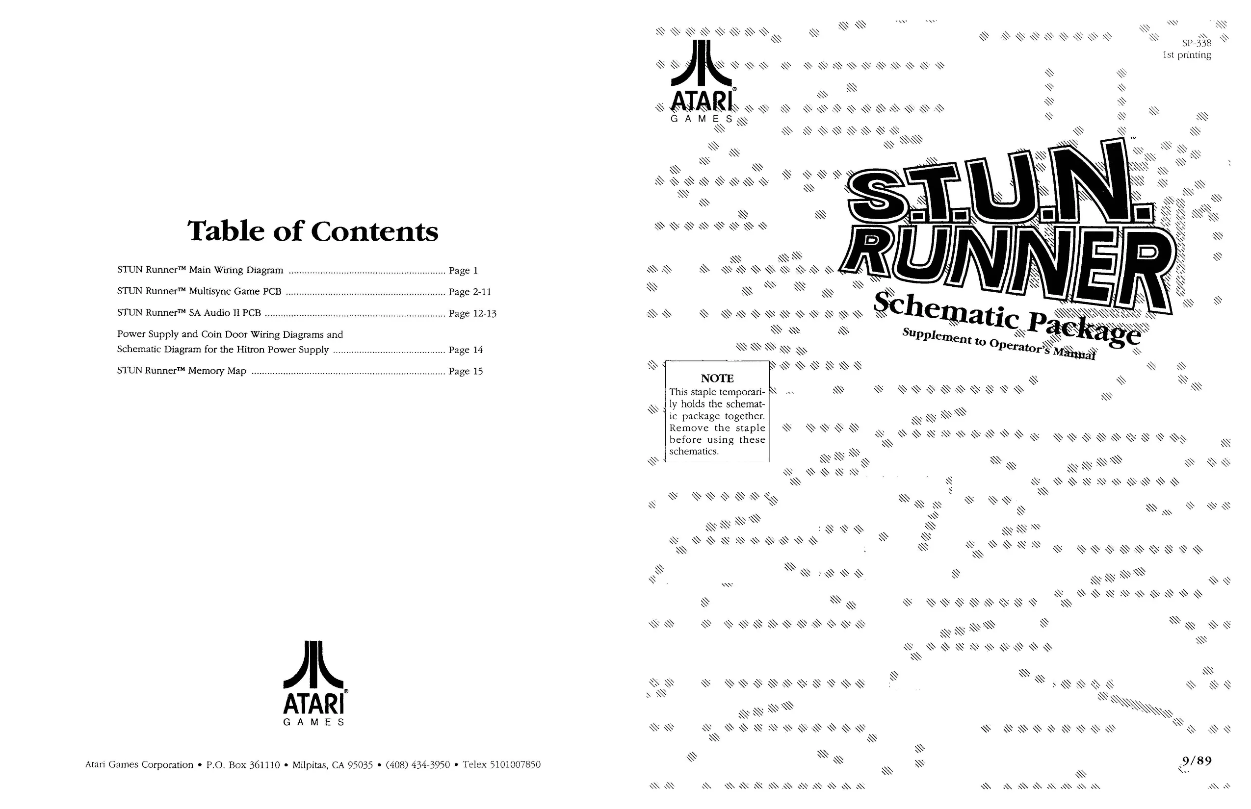
This page is a drawing, shown as the original scan.
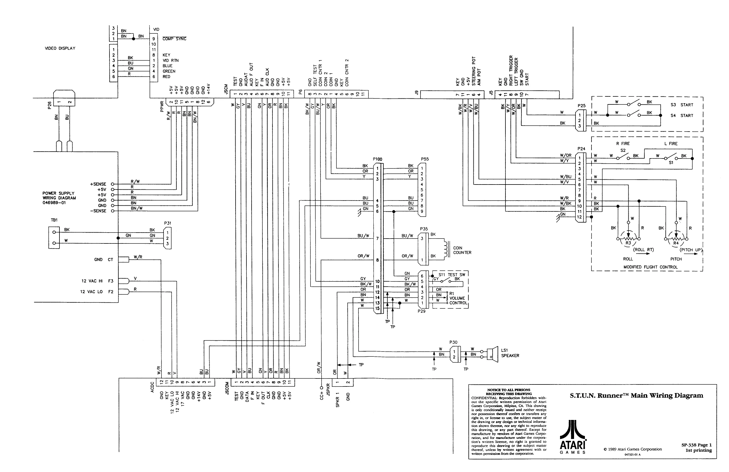
This page is a drawing, shown as the original scan.
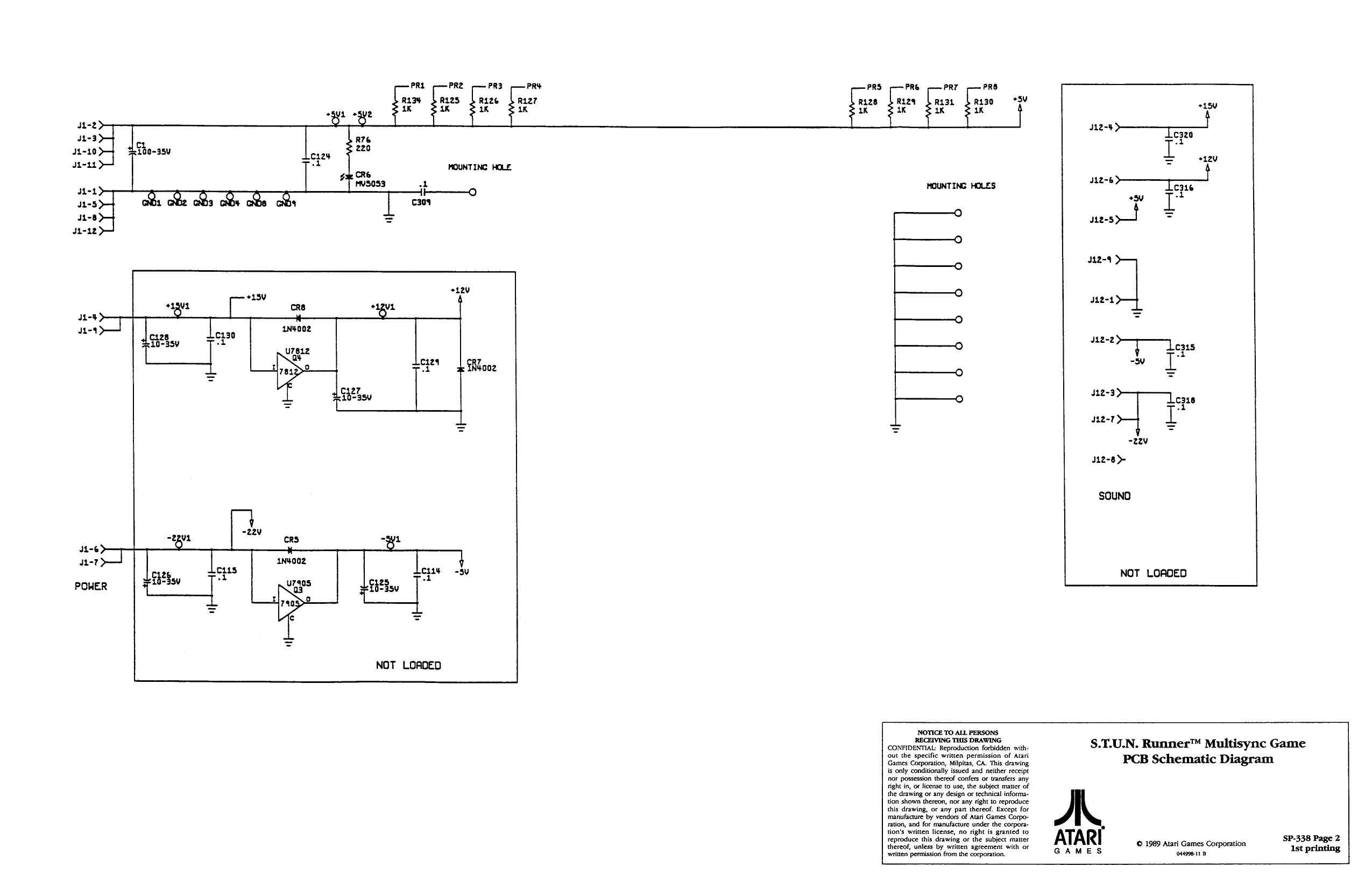
This page is a drawing, shown as the original scan.
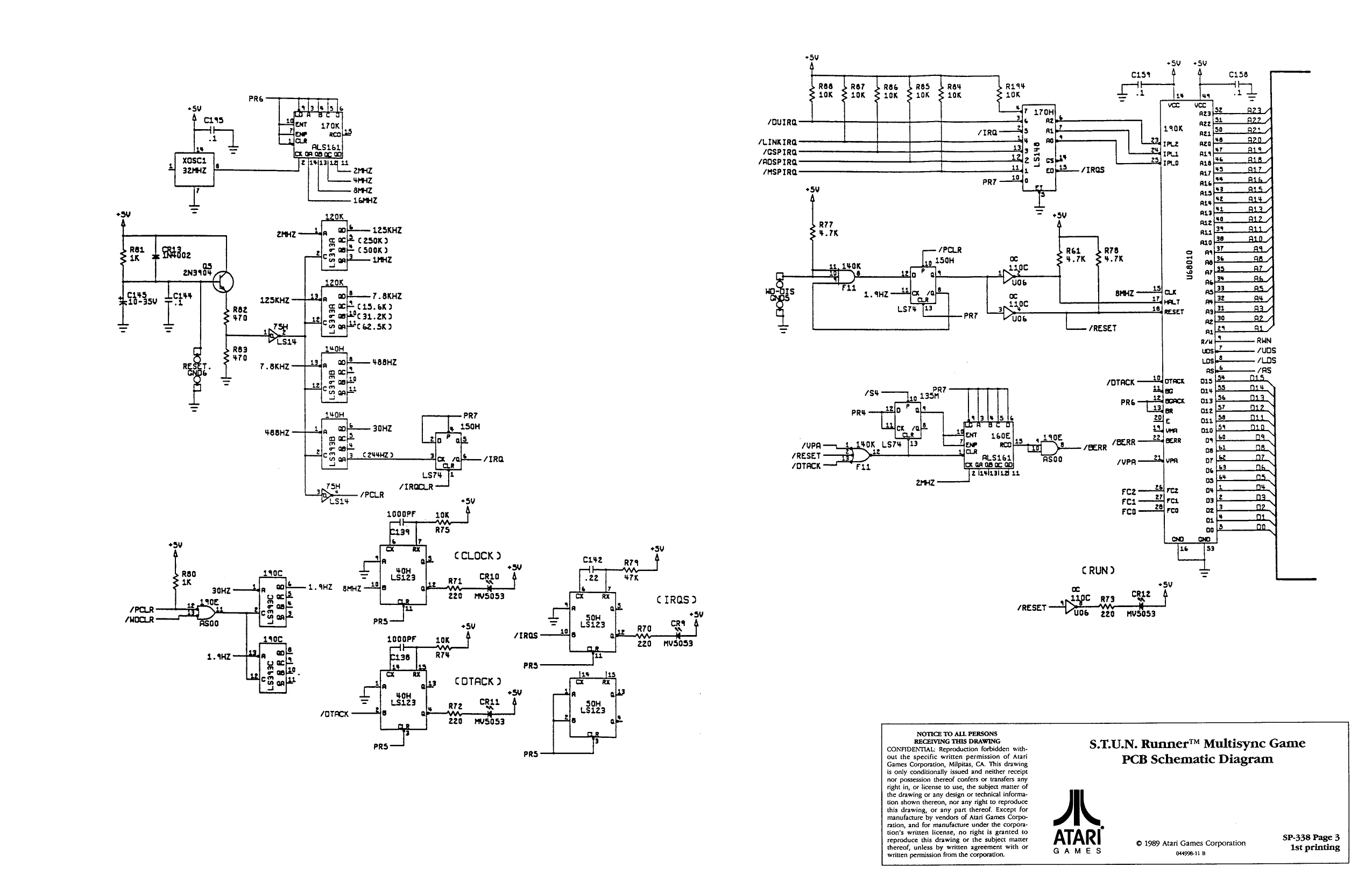
“su 4 su cise { ros rer Sree 194 40K 320K 3 10K 20K = ct 18 aaa ne : ia “ee
L2SKHZ 250K) CS00K) 68010
7OTACK ovec, ec PRE Bonck BR ee SS A /RERR BERR wpn—24a ven
es ree —24 Fea —24 rcs FCO 28 reo
CCLOCK 9
CRUND
RESET mY o ‘ Dike Wo nvsoss Sd ari CRO
mvS053
+Su . /tRas icooPr 10K
PRS
Sv
/OTACK
NOTICE TO ALL PERSONS RECEIVING THIS DRAWING
bid CONFIDENTIAL: Reproduction forbidden with- S.T.U.N. Runnet™ Multisync Game
Games cozporton, Mpls, CA Ths caving PCB Schematic Diagram 's only conditionally issued and neither receipt ‘nor possession thereof confers or transfers any
fightin, oF license to use, the subject matter of manufacture by vendors of Atari Games Corpo
the drawing or any design or technical information shown thereon, nor any right to reproduce this drawing, or any part thereof. Except for manufacture by vendors of Atari Games Corporation, and for manufacture under the corporatone ere fersesroe cece ATA thereof, unless by written agreement with or Sco oie ye , SP-338 Page 3 © 1989 Atari Ge Cor tion: GAMES womens por Ast printing
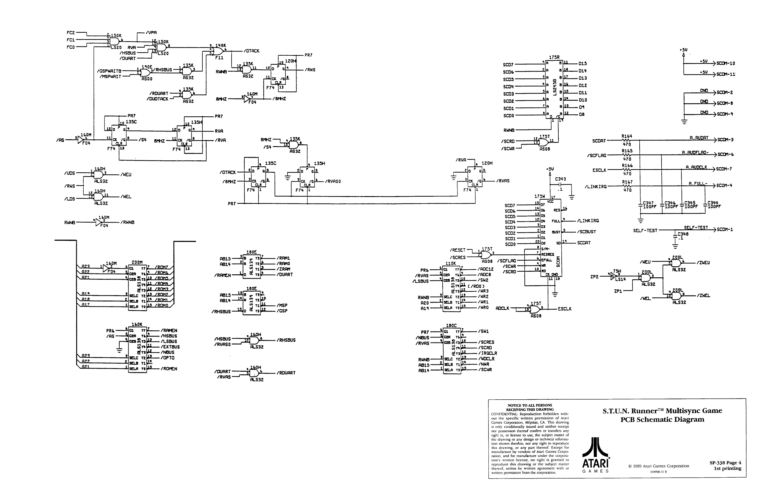
This page is a drawing, shown as the original scan.
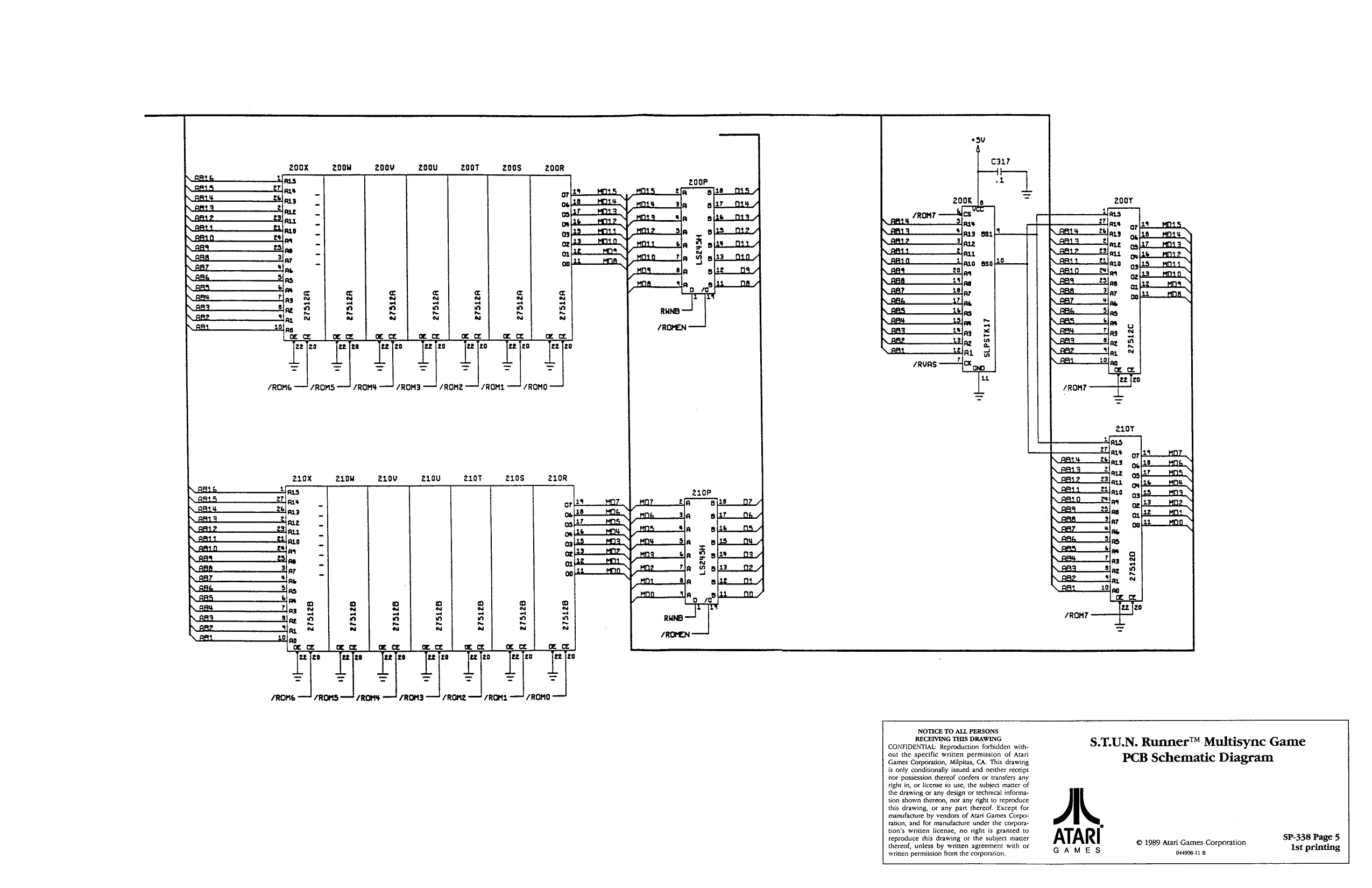
This page is a drawing, shown as the original scan.
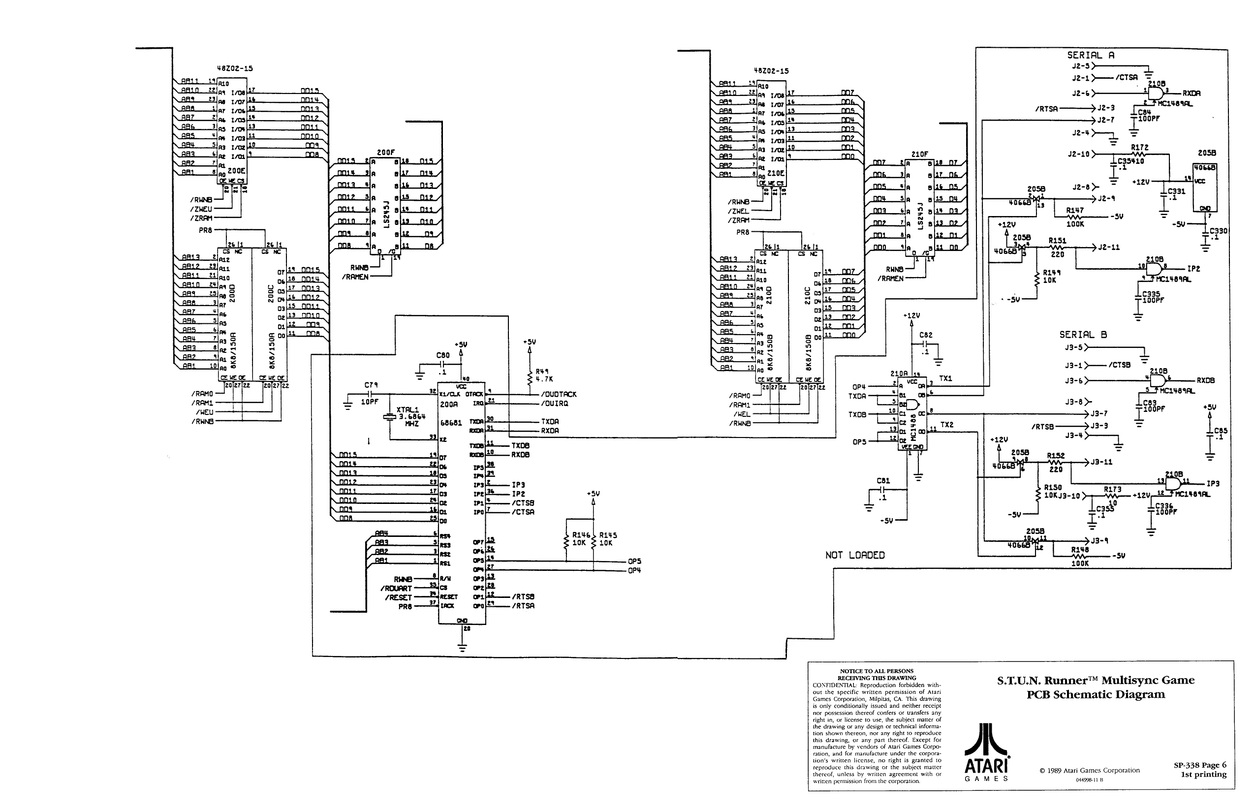
This page is a drawing, shown as the original scan.
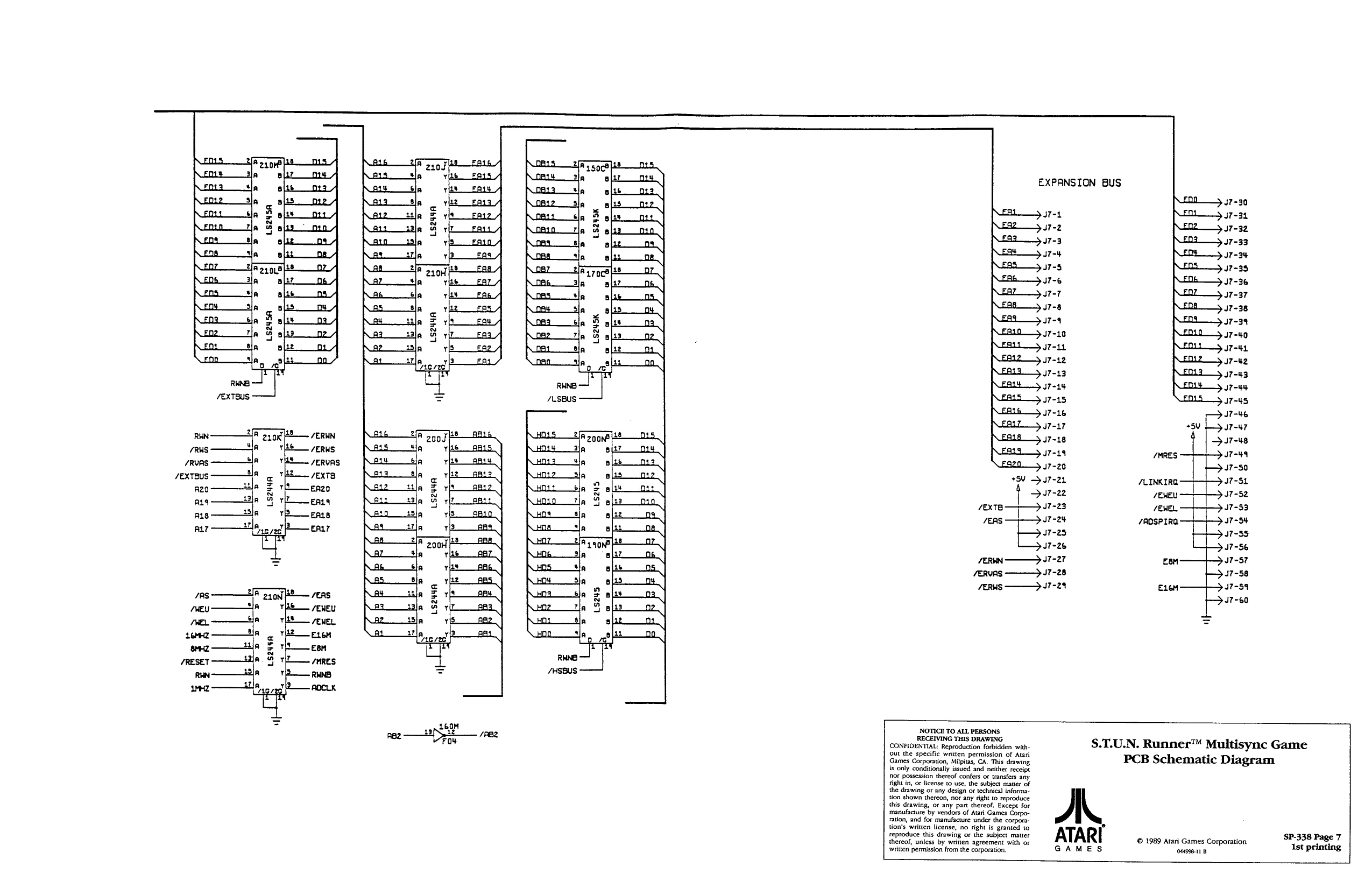
This page is a drawing, shown as the original scan.
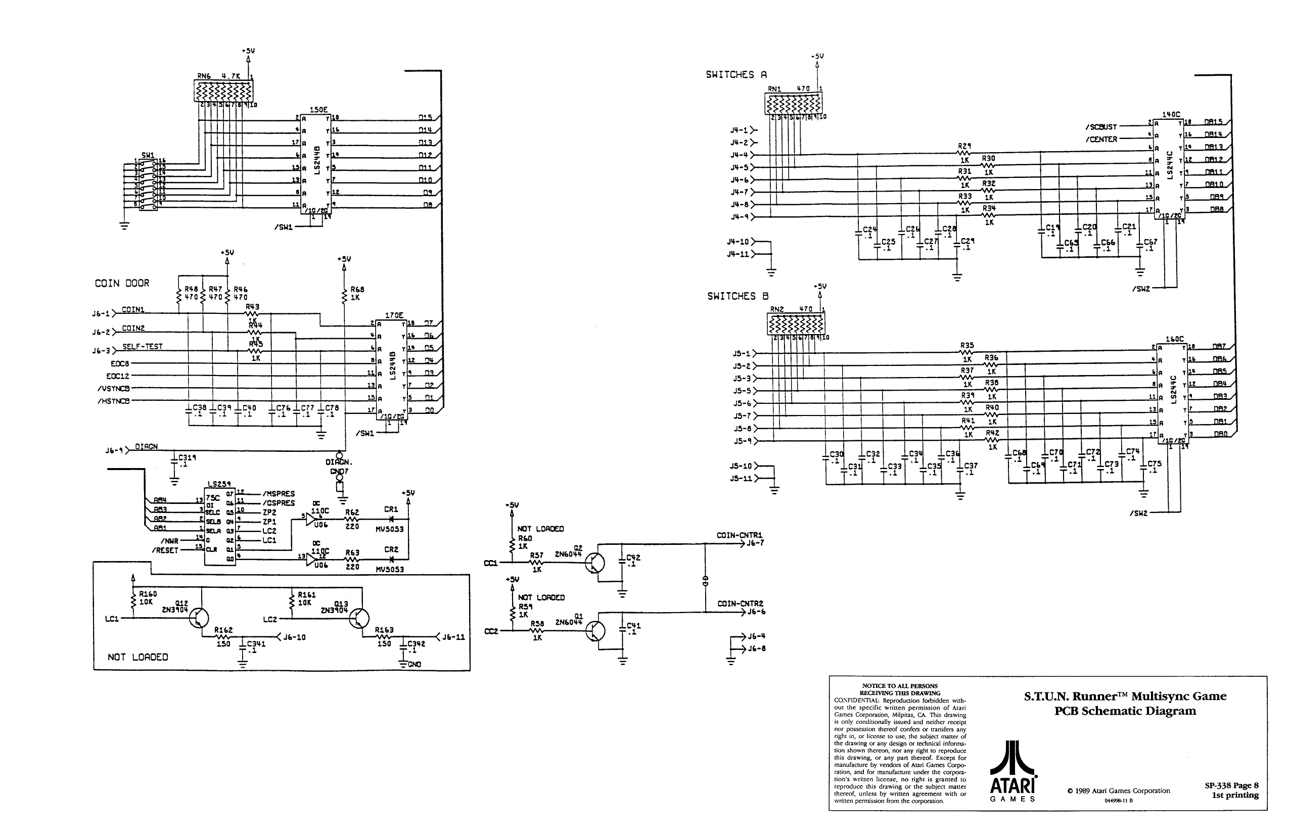
This page is a drawing, shown as the original scan.
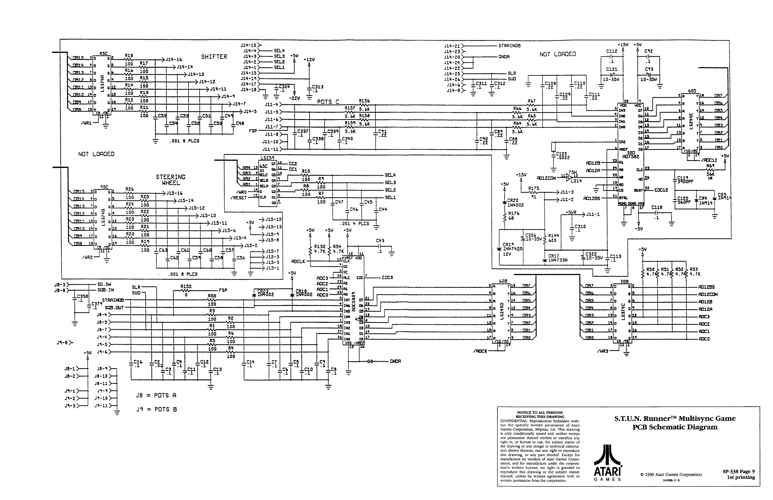
This page is a drawing, shown as the original scan.
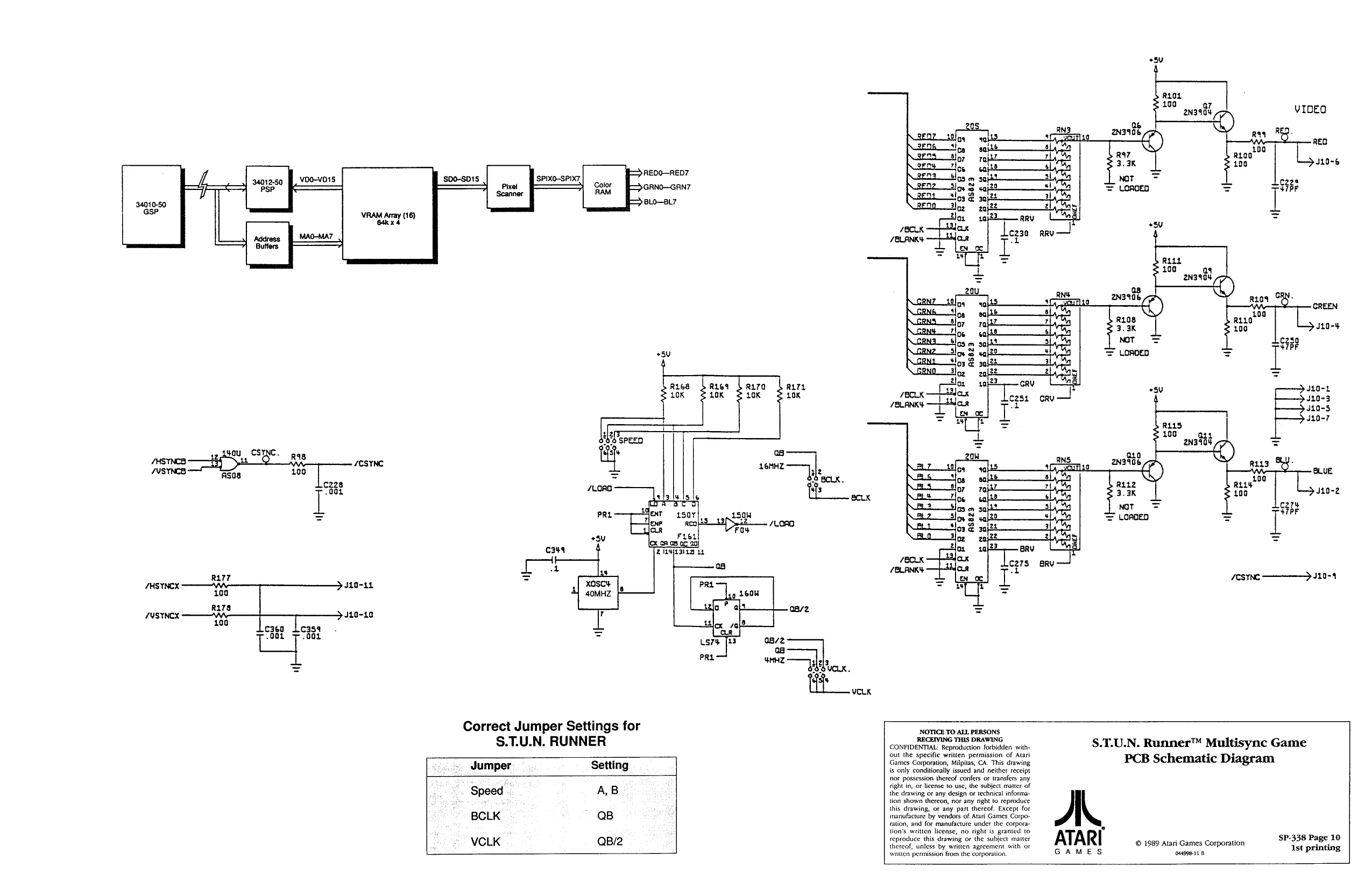
This page is a drawing, shown as the original scan.
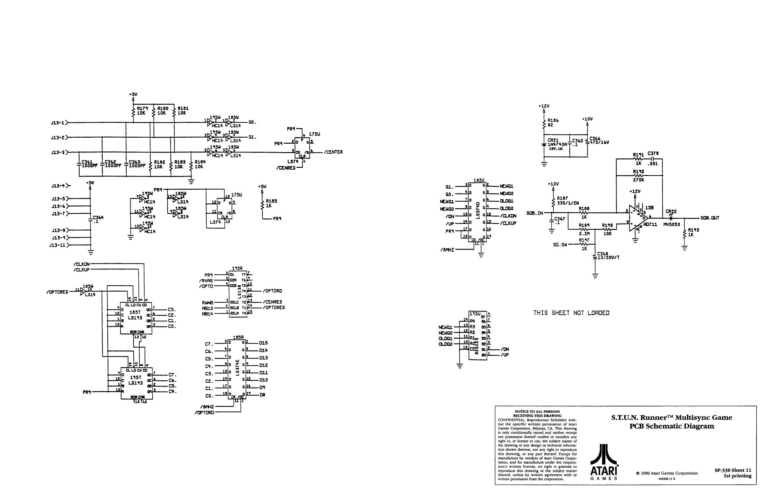
This page is a drawing, shown as the original scan.
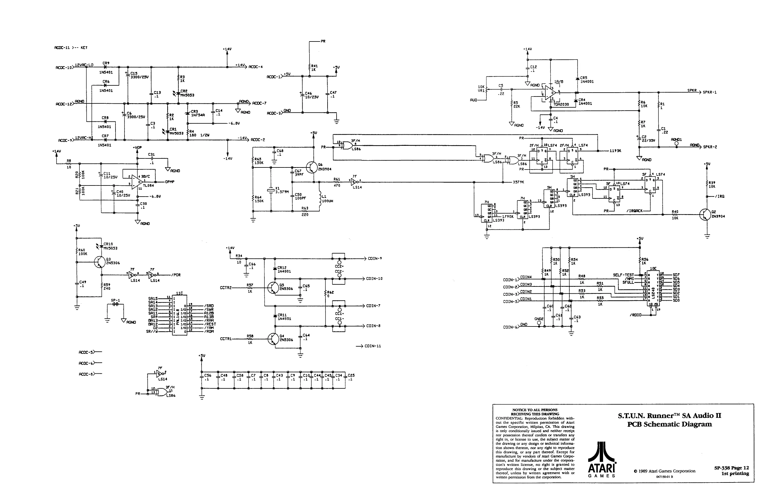
This page is a drawing, shown as the original scan.
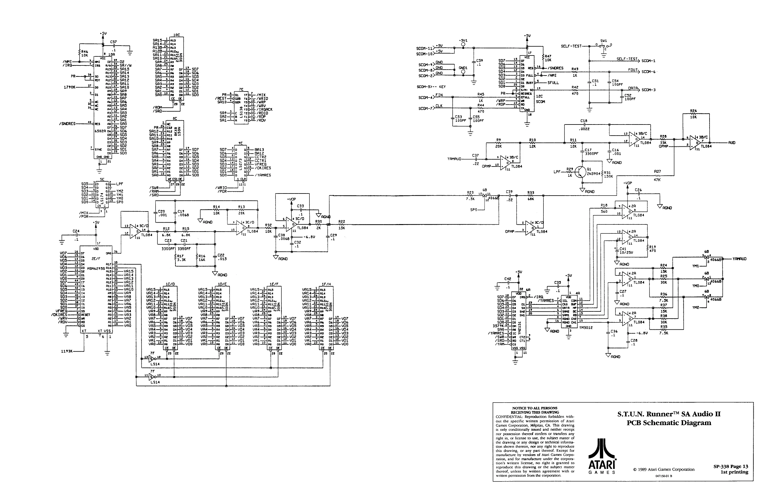
This page is a drawing, shown as the original scan.
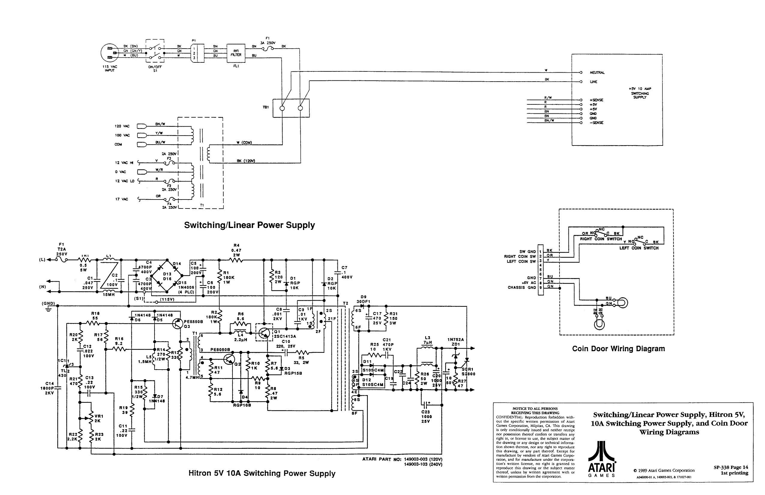
This page is a drawing, shown as the original scan.
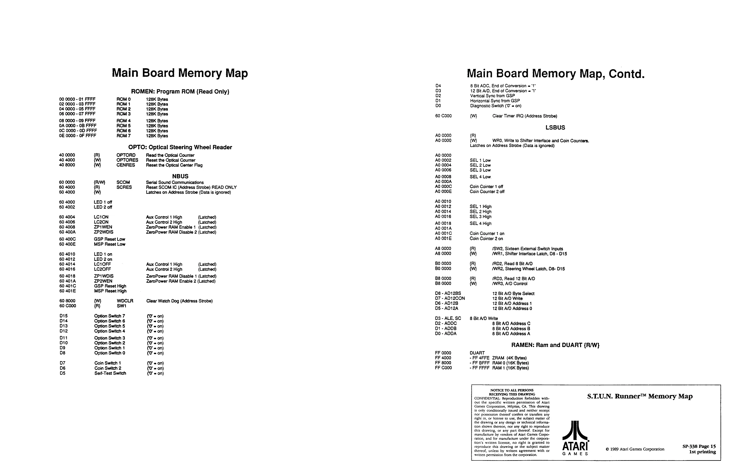
Main Board Memory Map
ROMEN: Program ROM {Read Only}
| 00 0000 - 01 FFFF | ROMO | 128K Bytes: |
| 02 0000 - 03 FFFF | ROM 1 | 128K Bytes: |
| 04 0000 - 05 FFFF | ROM 2 | 128K Bytes |
| 06 0000 - 07 FFFF | ROM3 | 128K Bytes: |
| 08 0000 - 09 FFFF | ROM 4 | 128K Bytes |
| 0A 0000 - OB FFFF | ROM 5 | 128K Bytes |
| OC 0000 - 0D FFFF | ROM6 | 128K Bytes |
| OE 0000 - OF FFFF | ROM7 | 128K Bytes |
60 0000 60 4000 60 4000 60 4002 60 4004 60 4006 60 400A 60 400C 60 400E
60 4010 60 4012 60 4014 60 4016 60 4018 60 401A 60 401C 60 401E
60 8000 60 CooO
O15, o14
p12
B10
o7
0S
OPTO: Optical Steering Wheel Reader
| {R} | OPTORD | —_Read the Optical Counter |
Ww OPTORES Reset the Optical Counter
| ww | CENRES | Reset the Optical Center Flag |
NBUS
| {RW | SCOM | Serial Sound Communications |
| {A} | SCRES | Reset SCOM IC (Address Strobe) READ ONLY |
™ Latches on Address Strobe (Data is ignored)
LED 1 off LED 2 off
| LC10N | ‘Aux Control 1 High | (Latched) |
LC20N ‘Aux Control 2 High (Latched)
ZP1WEN ZeroPower RAM Enable 1 (Latched)
ZP2WOIS ZeroPower RAM Disable 2 (Latched) GSP Reset Low MSP Reset Low
LED 1 on LED 2 0n
| LCtOFF | ‘Aux Control 1 High | (Latched) |
| LC20FF | ‘Aux Control 2 High | (Latched) |
ZP1WDIS ZeroPower RAM Disable 1 (Latched) ZP2WEN ZeroPower RAM Enable 2 (Latched) GSP Reset High MSP Reset High
| ™ | WOCLR | Clear Watch Dog (Address Strobe) |
{R} swt
Option Switch 7 (0' = on) Option Switch 6 (0 = on) Option Switch 5 (0 = on) Option Switch 4 (0 = on) Option Switch 3 (0 = on) Option Switch 2 (0 = on) ‘Option Switch 1 (0° = on) Ontion Switch 0 (0 = on)
Coin Switch 1 (0 = on) Coin Switch 2 (0 = on) Seit-Test Switch (0' = on) 60 C000
AQ 0000 AO 0000
‘Ao 0000 ‘AQ 0002 ‘AO 0004 ‘AO 0006 AO 0008 AQ 000A AO 000C AQ 000E
‘AQ 0010 ‘0.0012 A0 0014 ‘A0 0016 A0 0018 AQ 001A AO 001C AO 001E A8 0000 A8 0000 Bo 0000 Bo 0000
88 0000 B8 0000
08 - AD12BS. 07 - AD12CON D6 - AD12B DS -AD12A
03 - ALE, SC D2 - ADDC 01 -ADDB (00 - ADDA
FF 0000 FF 4000 FF 8000 FF C000 Main Board Memory Map, Contd. 8 Bit ADC, End of Conversion = ‘t" 12 Bit A/D, End of Conversion = ‘1° Vertical Sync from GSP Horizontal Syne from GSP Diagnostic Switch (‘0° = on)
™ Clear Timer IRQ (Address Strobe)
LSBUS {R) WRO, Write to Shifter interface and Coin Counters. Latches on Address Strobe (Data is ignored)
SEL 1 Low SEL 2 Low SEL 3 Low SEL 4 Low
Coin Cointer 1 off Coin Counter 2 off
SEL 1 High SEL 2 High SEL 3 High SEL 4 High
Coin Counter 1 on Coin Cointer 2 on
(R) 1SW2, Sixteen External Switch Inputs wW, ‘WRI, Shifter Interface Latch, D8 - D15 (R) /RD2, Read 8 Bit A/D mw AWR2, Steering Wheel Latch, D8- 15 {R) /RD3, Read 12 Bit AD ‘/ANR3, A/D Control
12 Bit A/D Byte Select 12 Bit A/D Write 12 Bit AD Address 1 12 Bit AD Address 0
8 Bit A/D Write 8 Bit A/D Address C 8 Bit A/D Address B 8 Bit A/D Address A
RAMEN: Ram and DUART {R/W} QUART
- FF 4FFE ZRAM (4K Bytes)
- FE BFF RAM 0 (16K Bytes) -FF FFFF RAM 1 (16K Bytes)
NOTICE TO ALL PERSONS RECEIVING THIS DRAWING CONFIDENTIAL: Reproduction forbidden without the specific written permission of Atari Games Corporation, Milpitas, CA. This drawing is only conditionally issued and neither receipt Ror possession thereof confers or transfers any right in, of license to use, the subject matter of the drawing or any design or technical information shown thereon, nor any right to reproduce this drawing, or any part thereof. Except for manufacture by vendors of Atari Games Corporation, and for manufacture under the corpora tion’s written license, no right is granted to. "a
thereof, unless by writen agreement with or ‘written permission from the corporation. GAMES © 1989 Atari Games Corporation S.T.U.N. Runner™ Memory Map
SP-338 Page 15, 1st printing