Pole Position SP-218 5th Printing
Pole Position (World) (Namco, 1982) · Schematic Package · 32 pages · 68 sections · original scan
Sheet 1A
Sheet 1B
Sheet 2A
Sheet 2B
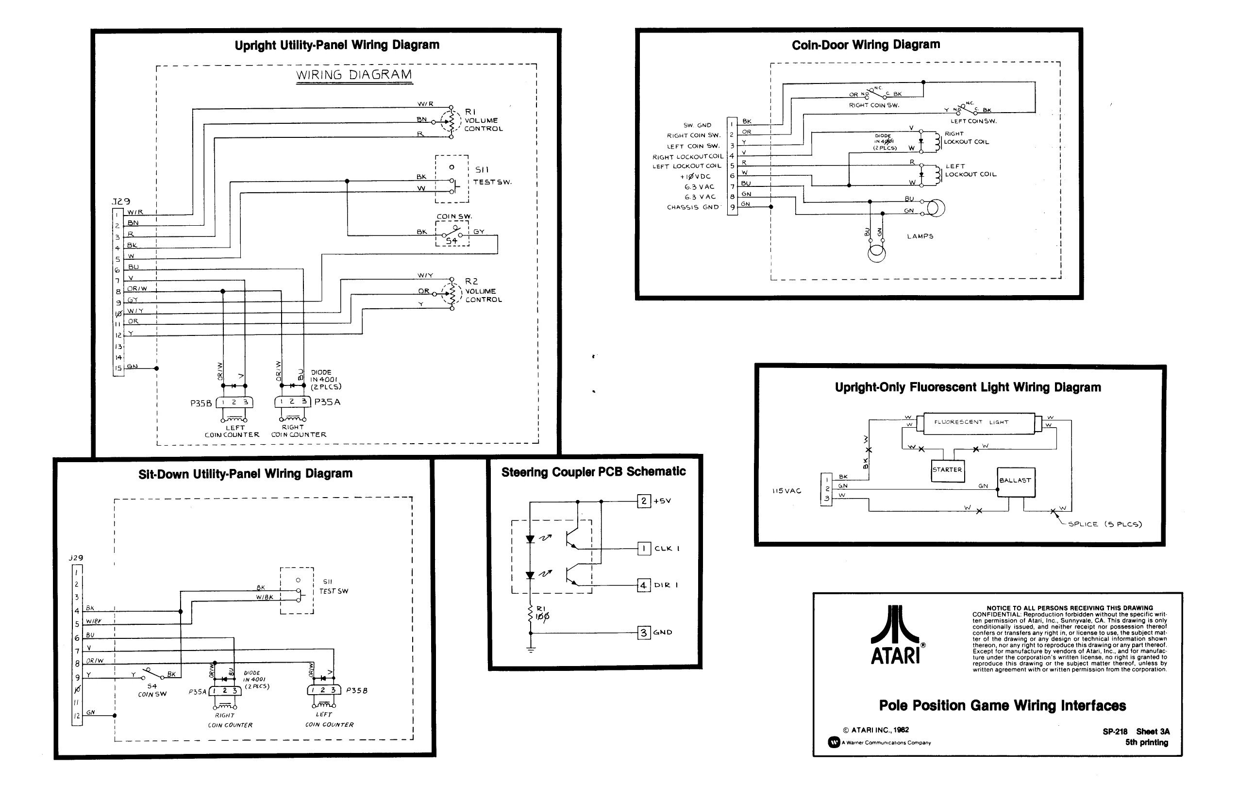
Sheet 3A
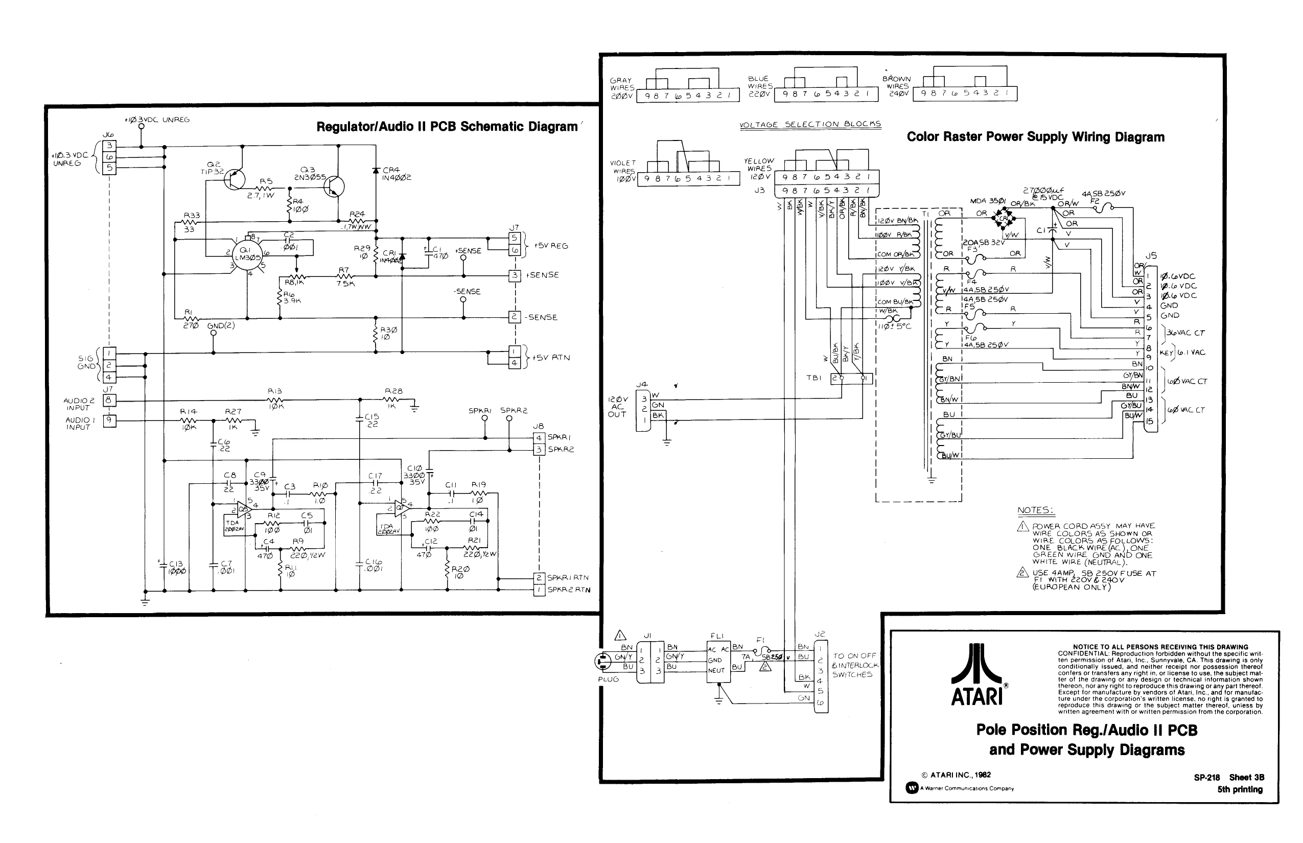
Sheet 3B
Sheet 4A
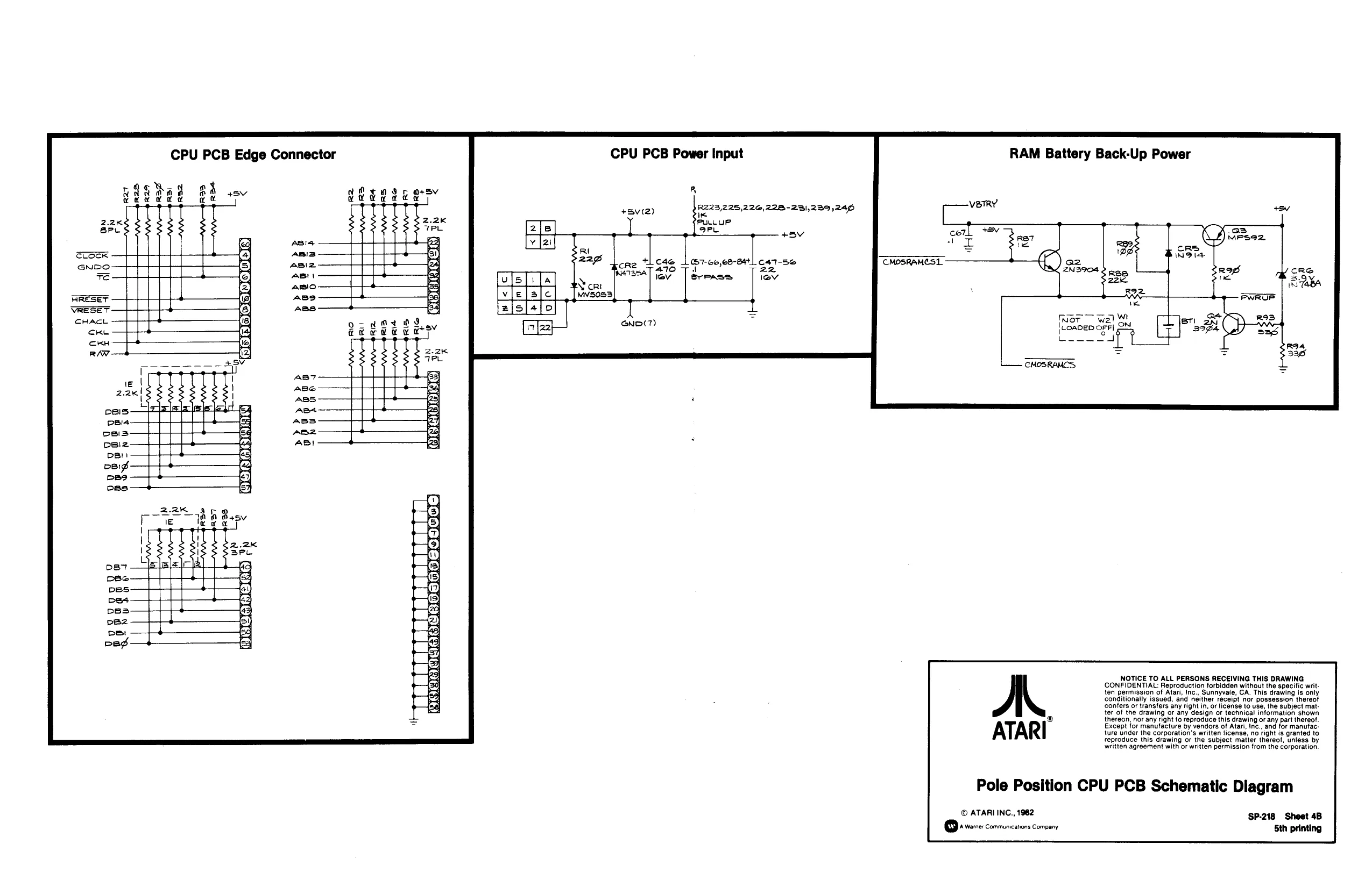
Sheet 4B Sheet 5A Sheet 5B Sheet 6A Sheet 6B Sheet 7A Sheet 7B Sheet 8A Sheet 8B Sheet 9A Sheet 9B Sheet 10A
Sheet 10B Sheet 114 Sheet 11B
Sheet 12A Sheet 12B Sheet 13A Sheet 13B Sheet 144 Sheet 14B Sheet 15A Sheet 15B
Sheet 16A
Sheet 16B Table of Contents
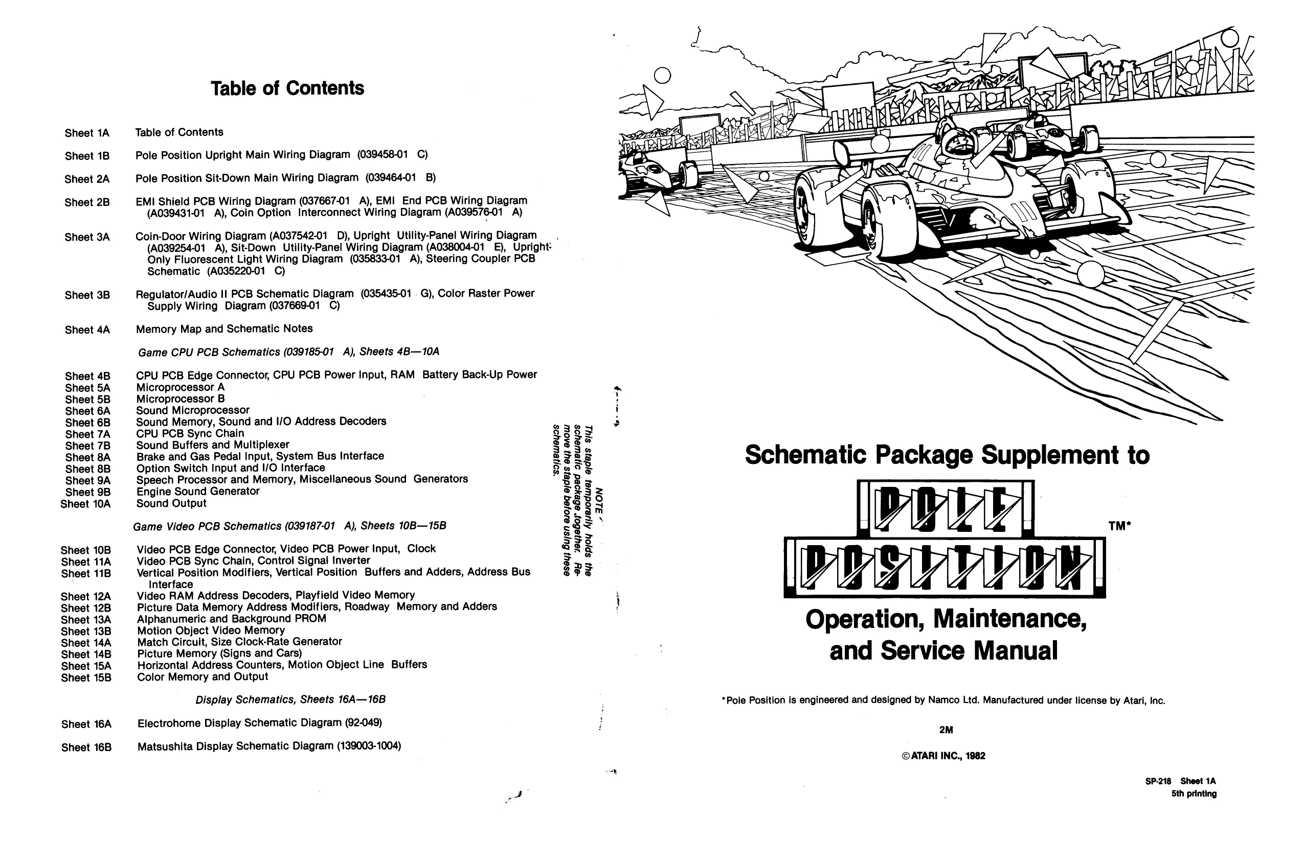
Table of Contents
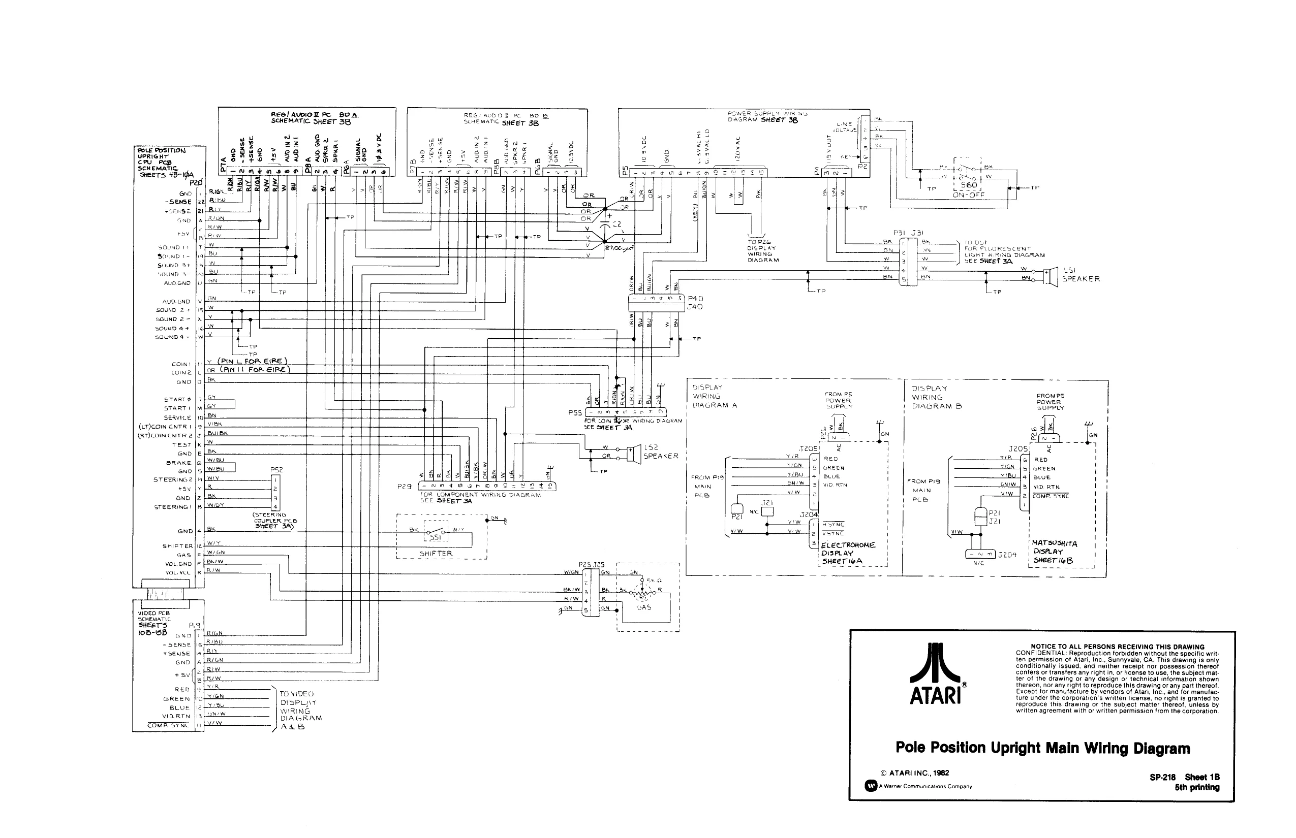
Pole Position Upright Main Wiring Diagram (039458-01 C)
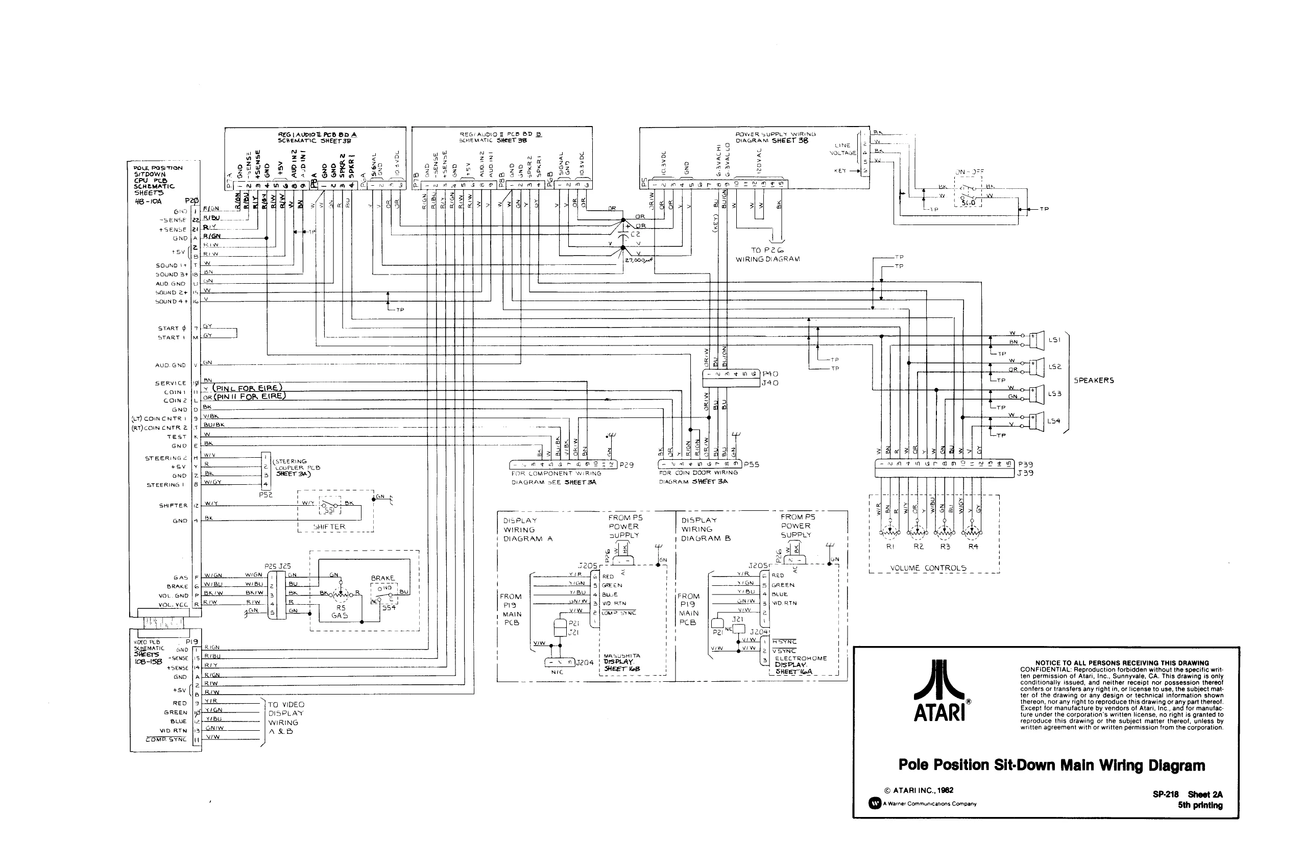
Pole Position Sit-Down Main Wiring Diagram (039464-01 B)
EMI Shield PCB Wiring Diagram (037667-01 A), EMI End PCB Wiring Diagram (A039431-01 A), Coin Option Interconnect Wiring Diagram (A039576-01 A)
Coin-Door Wiring Diagram (A037542-01 D), Upright Utility-Panel Wiring Diagram (A039254-01 A), Sit-Down Utility-Panel Wiring Diagram (A038004-01 E), Upright* Only Fluorescent Light Wiring Diagram (035833-01 A), Steering Coupler PCB Schematic (A035220-01 C)
Regulator/Audio Il PCB Schematic Diagram (035435-01 . G), Color Raster Power Supply Wiring Diagram (037669-01 C)
Memory Map and Schematic Notes
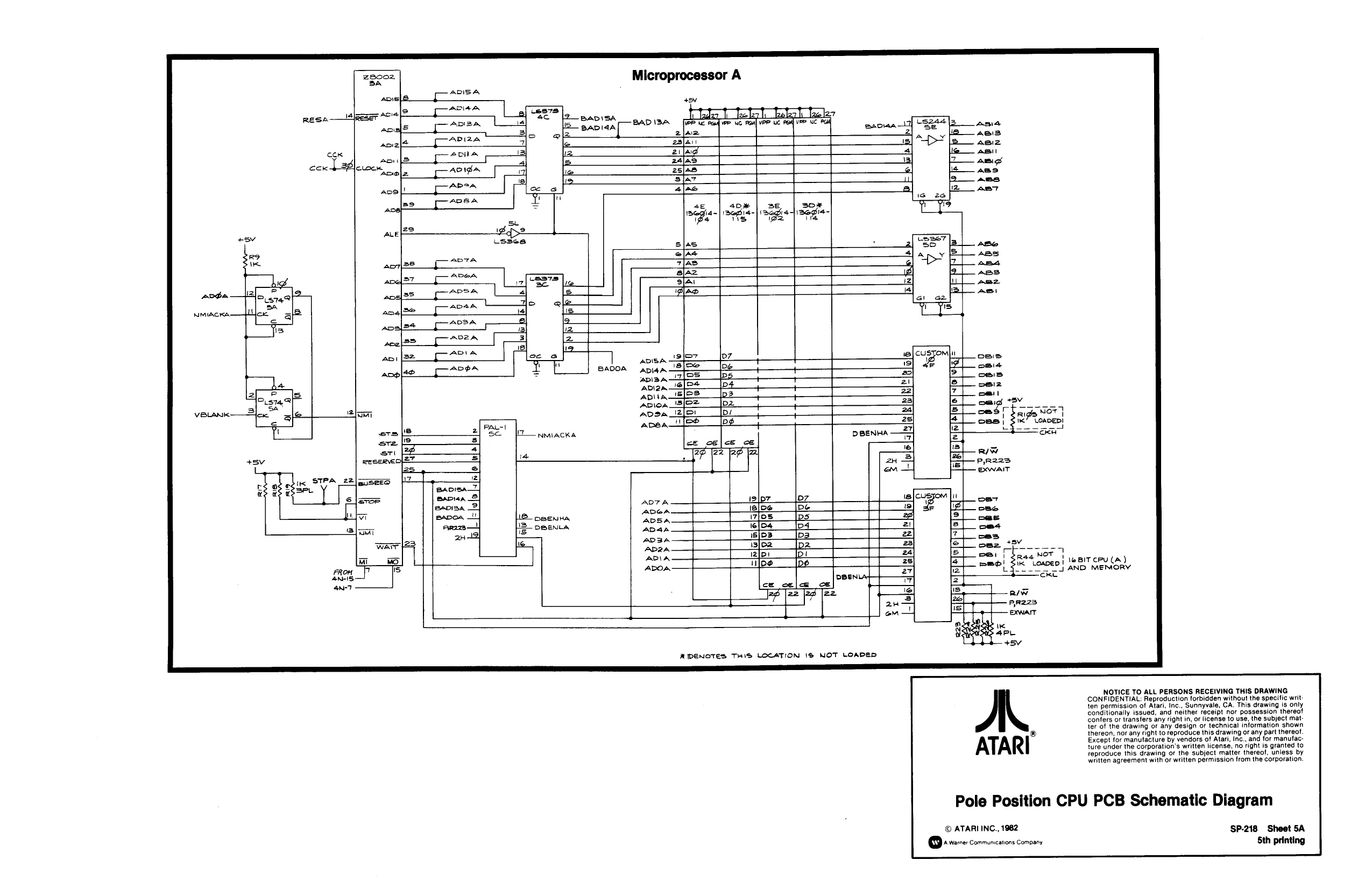
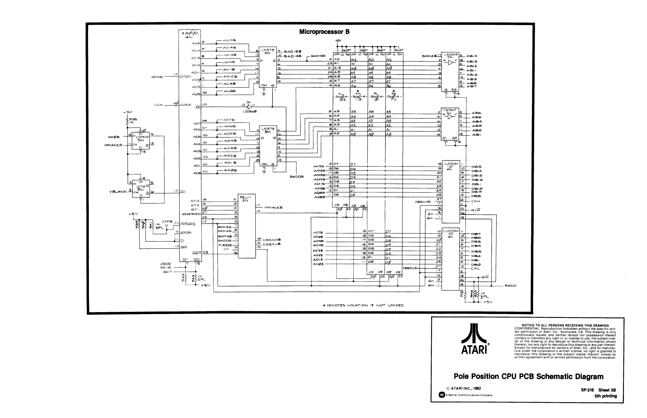
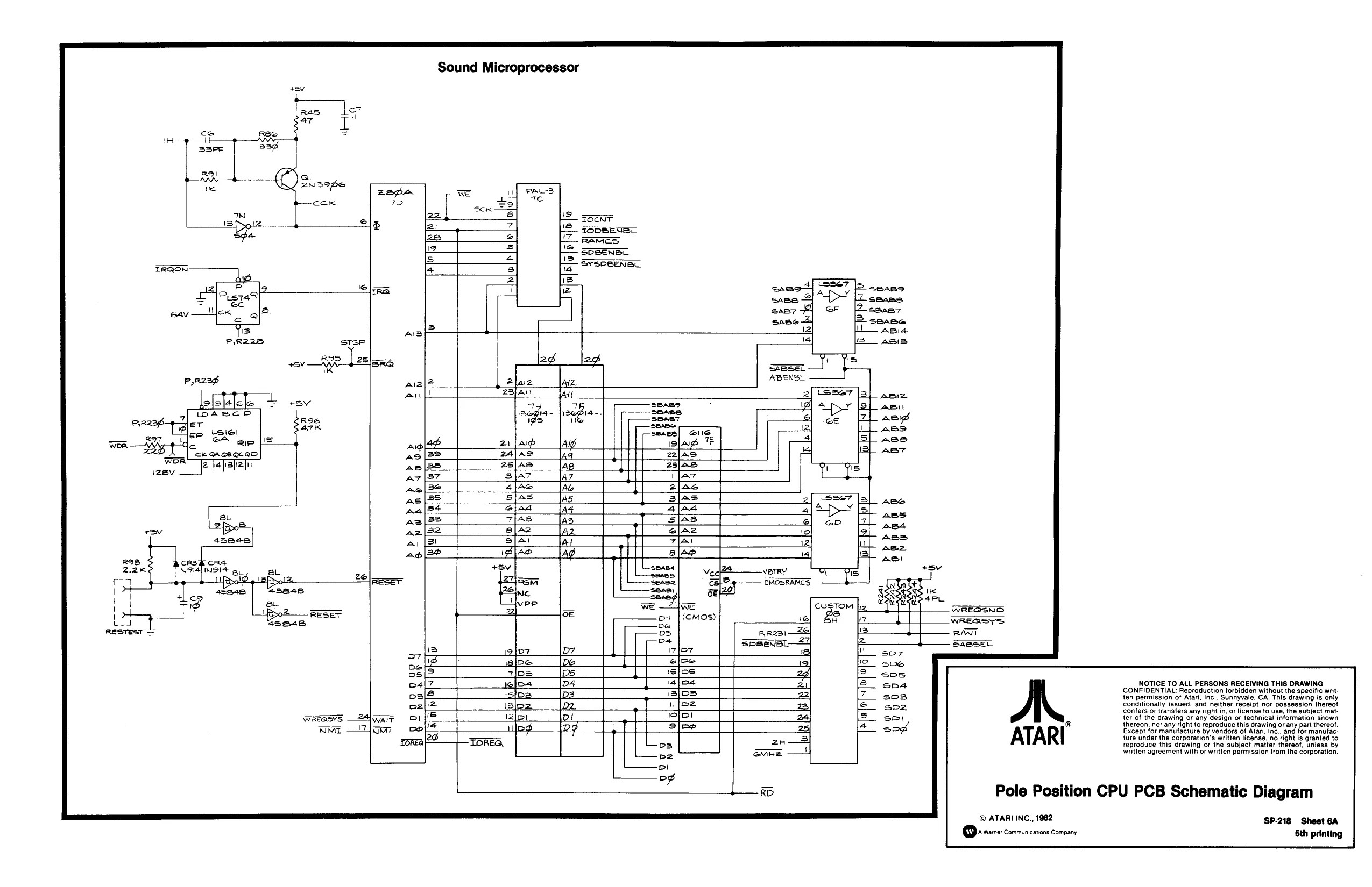
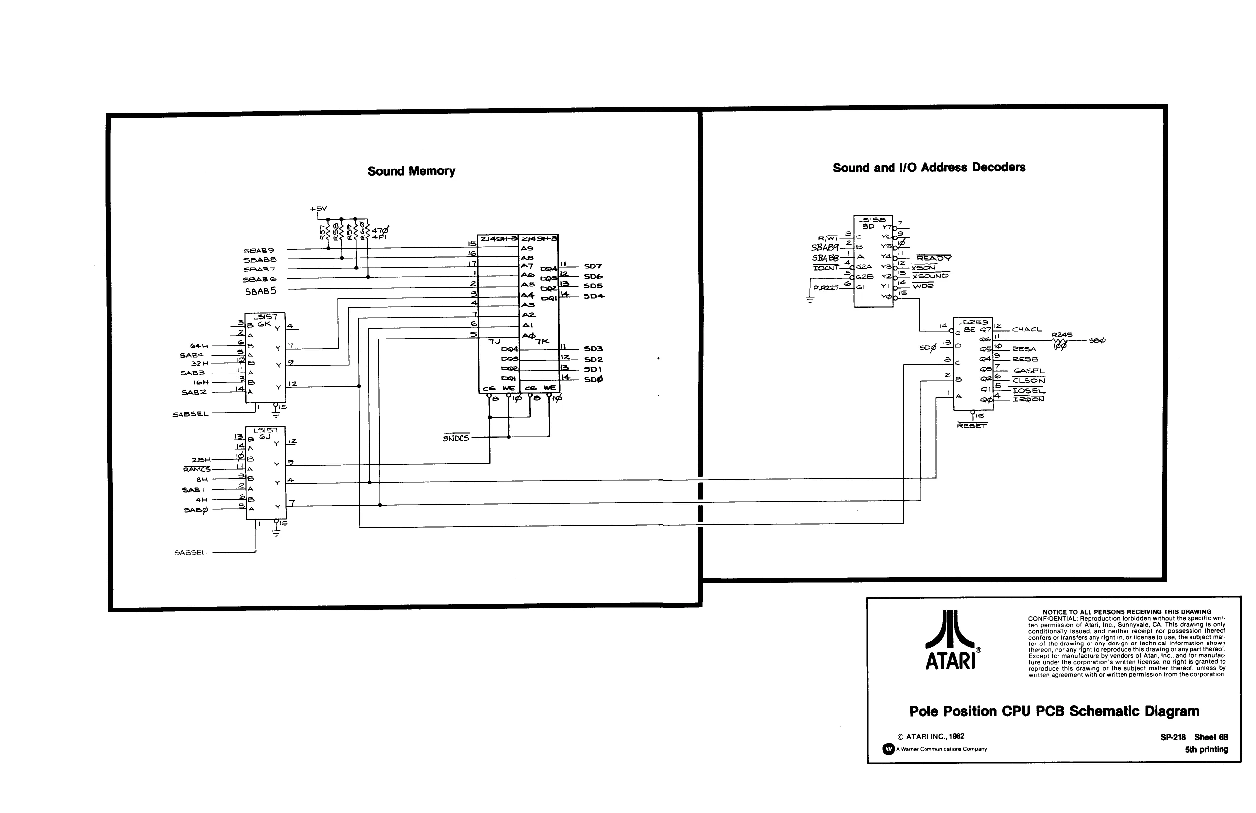
Game CPU PCB Schematics (039185-01 A), Sheets 4B—10A
CPU PCB Edge Connector, CPU PCB Power Input, RAM Battery Back-Up Power Microprocessor A Microprocessor B Sound Microprocessor Sound Memory, Sound and I/O Address Decoders CPU PCB Sync Chain Sound Buffers and Multiplexer Brake and Gas Pedal Input, System Bus Interface Option Switch Input and I/O Interface Speech Processor and Memory, Miscellaneous Sound Generators Engine Sound Generator Sound Output “soneweyos esey) Busn es0jeq ejde}s ay} aAOW -0y veyjeBoy abeyoed oewayos
Game Video PCB Schematics (039187-01 A), Sheets 10B—15B
Video PCB Edge Connector, Video PCB Power Input, Clock Video PCB Sync Chain, Control Signal Inverter Vertical Position Modifiers, Vertical Position Buffers and Adders, Address Bus Interface Video RAM Address Decoders, Playfield Video Memory Picture Data Memory Address Modifiers, Roadway Memory and Adders ! 7 . Alphanumeric and Background PROM oer pet arraee Operation, Maintenance, Match Circuit, Size Clock-Rate Generator . d . M I Picture Memory (Signs and Cars) Se Horizontal Address Counters, Motion Object Line Buffers an rvice anua Color Memory and Output ey) spjoy Aysesoduies ajdeis siyt
+ ALON
Display Schematics, Sheets 16A—16B : *Pole Position is engineered and designed by Namco Ltd. Manufactured under license by Atari, Inc.
Electrohome Display Schematic Diagram (92-049) } 2M
Matsushita Display Schematic Diagram (139003-1004) ©ATARI INC., 1982
SP-218 Sheet 1A a Sth printing
This page is a drawing, shown as the original scan.
This page is a drawing, shown as the original scan.
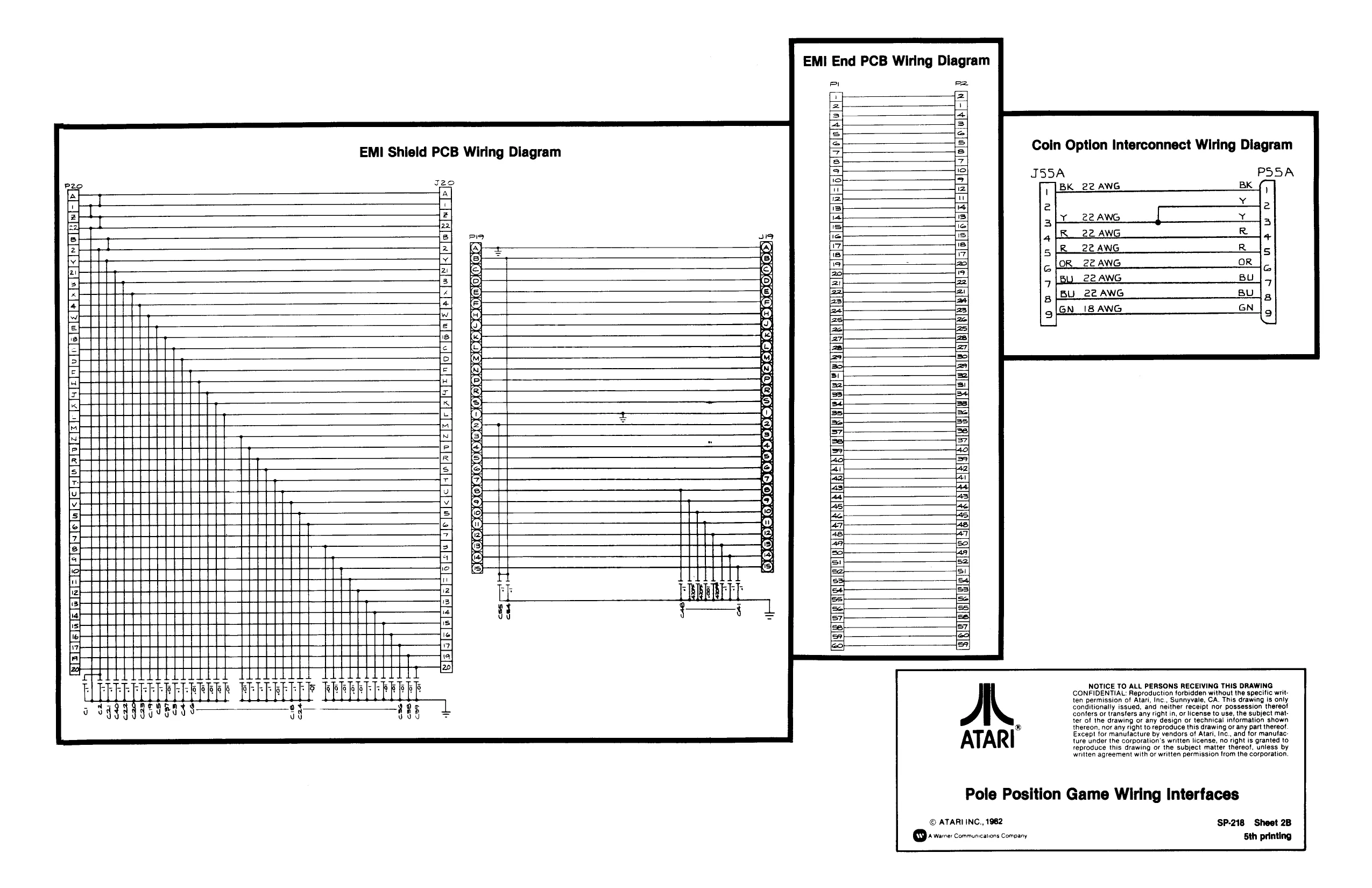
EMI Shield PCB Wiring Diagram
v
EMI End PCB Wiring Diagram
Coin Option Interconnect Wiring Diagram
HOROOSOOE fois [ofuloups]-Ty] B
JI55A PS5A
OR 22 AWG
5 22 AWG
Bu 22 AWG
GN_ 18 AWG way nurawn ono oNntuUN —
BRT TBTS P20 J2o A A ira z 144 [=a a2 eS S zt z iv ¥ [st 3 x Z lat 4 hw Ww = 1=] s rH fe] [=] a [>} o F J a iz] eal = « is [S4] tL
Ma N
e [a] S 7444 [2] v = ©
fa BRU REGHGE
RENEE
NG
NOTICE TO ALL PERSONS RECEIVING THIS DRAWING CONFIDENTIAL: Reproduction forbidden without the specific written permission of Atari, Inc., Sunnyvale, CA. This drawing is only conditionally issued, and neither receipt nor possession thereo! confers or transfers any right in, or license to use, the subject matter of the drawing or any design or technical information shown ® thereon, nor any right to reproduce this drawing or any part thereof. Except for manufacture by vendors of Atari, Inc., and for manufac: ture under the corporation's written license, no right is granted to reproduce this drawing or the subject matter thereof, unless by written agreement with or written permission from the corporation.
Pole Position Game Wiring Interfaces
© ATARI INC., 1982 SP-218 Sheet 2B
Qrvere: Communications Company Sth printing
This page is a drawing, shown as the original scan.
This page is a drawing, shown as the original scan.
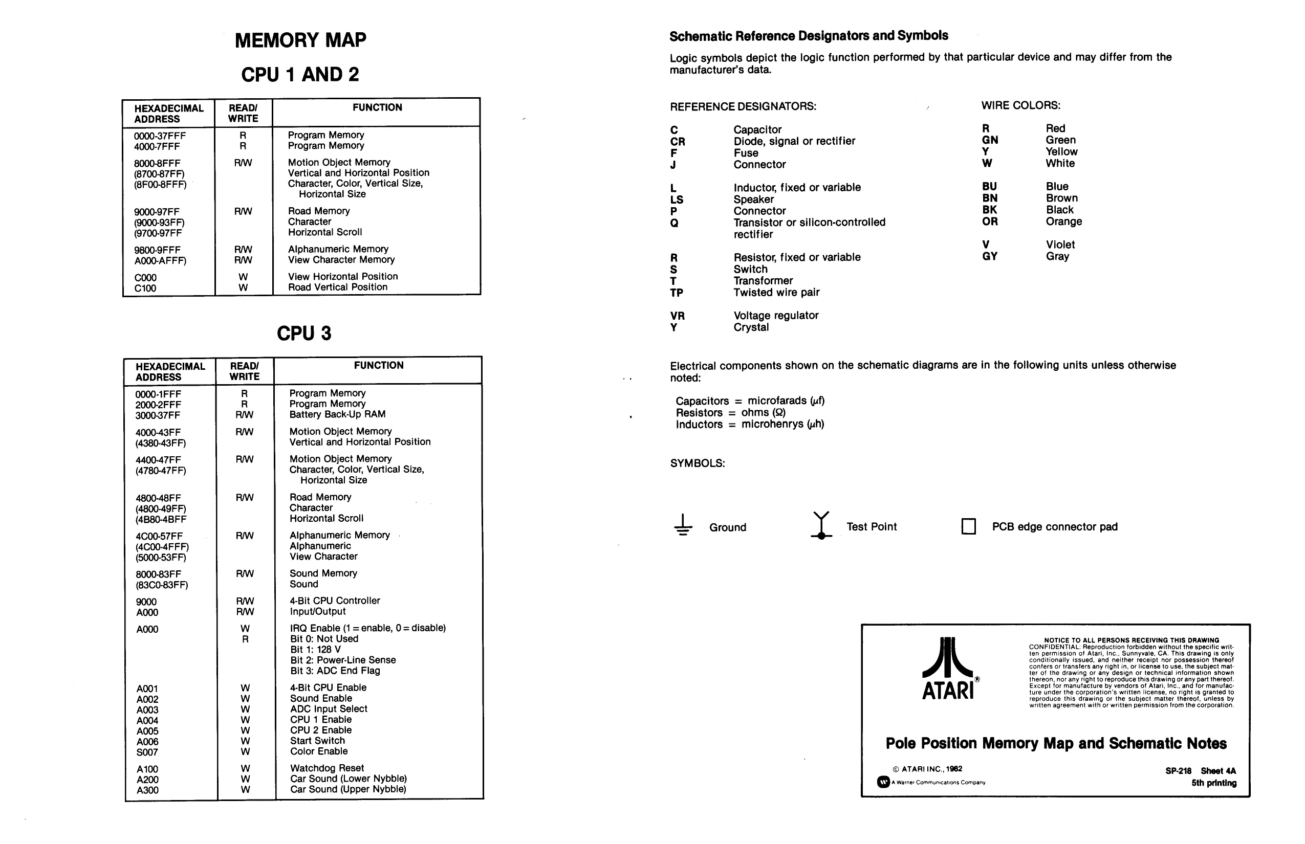
MEMORY MAP
CPU 1 AND 2
IEXADECIMAL
ADDRESS WRITE
0000-37FFF Program Memory 4000-7FFF Program Memory 8000-8FFF Motion Object Memory (8700-87FF) Vertical and Horizontal Position (8F00-8F FF) Character, Color, Vertical Size, Horizontal Size
Road Memory 9000-97FF (9000-93FF) Character (9700-97FF Horizontal Scroll 9800-9F FF Alphanumeric Memory
A000-AFFF) View Character Memory
C000 View Horizontal Position
C100 Road Vertical Position
CPU 3
HEXADECIMAL READ/ FUNCTION
0000-1FFF Program Memory 2000-2FFF Program Memory 3000-37FF Battery Back-Up RAM 4000-43FF (4380-43FF) 4400-47FF (4780-47 FF) Motion Object Memory Vertical and Horizontal Position
Motion Object Memory Character, Color, Vertical Size, Horizontal Size 4800-48FF Road Memory (4800-49FF) Character (4B80-4BFF Horizontal Scroll 4C00-57FF Alphanumeric Memory (4C00-4FFF) Alphanumeric (5000-53FF) View Character 8000-83FF Sound Memory (83C0-83FF) Sound 9000 4-Bit CPU Controller A000 Input/Output IRQ Enable (1 = enable, 0 = disable) Bit 0: Not Used Bit 1: 128 V Bit 2: Power-Line Sense Bit 3: ADC End Flag 4-Bit CPU Enable Sound Enable ADC Input Select CPU 1 Enable CPU 2 Enable Start Switch Color Enable
Watchdog Reset Car Sound (Lower Nybble) Car Sound (Upper Nybble) SSS SSSSSS= Schematic Reference Designators and Symbols
Logic symbols depict the logic function performed by that particular device and may differ from the manufacturer's data.
REFERENCE DESIGNATORS:
c Capacitor CR Diode, signal or rectifier F Fuse J Connector
L Inductor, fixed or variable Ls Speaker P Connector Q Transistor or silicon-controtled rectifier
R Resistor, fixed or variable Ss Switch T Transformer TP Twisted wire pair
VR Voltage regulator Y Crystal WIRE COLORS:
R Red GN Green Y Yellow Ww White
BU Blue BN Brown BK Black OR Orange
Vv Violet GY Gray
Electrical components shown on the schematic diagrams are in the following units unless otherwise noted:
Capacitors = microfarads (uf) Resistors = ohms (Q) Inductors = microhenrys (uh)
SYMBOLS:
Lt Ground Test Point oO PCB edge connector pad
NOTICE TO ALL PERSONS RECEIVING THIS DRAWING CONFIDENTIAL: Reproduction forbidden without the specific written permission of Atari, Inc., Sunnyvale, CA. This drawing is only conditionally issued, and neither receipt nor possession thereof confers or transfers any right in, or license to use, the subject matter of the drawing or any design or technical information shown thereon, nor any right to reproduce this drawing or any part thereof. Except for manufacture by vendors of Atari, Inc., and for manutacture under the corporation's written license, no right is granted to reproduce this drawing or the subject matter thereof, unless by written agreement with or written permission from the corporation.
Pole Position Memory Map and Schematic Notes
© ATARI INC., 1962 ‘SP-218 Sheet 4A 5th printing
ew
CPU PCB Edge Connector
CPU PCB Power Input
+5V(2) iy
PULL UP PL
Srrass. R223,225,22@,22B-231,239,245 he
+5vV reson] c47-5e 22. lov
RAM Battery Back-Up Power
22ic Rez
Ve
NT) wal WI [LOADED OFFI u---
CMOSRAMCS
NOTICE TO ALL PERSONS RECEIVING THIS DRAWING CONFIDENTIAL: Reproduction forbidden without the specific written permission of Atari, Inc., Sunnyvale, CA. This drawing is only conditionally issued, and neither receipt nor possession thereof conters or transfers any right in, or license to use, the subject matter of the drawing or any design or technical information shown ® thereon, nor any right to reproduce this drawing or any part thereof. Except for manufacture by vendors of Atari, Inc., and for manufacture Under the corporation's written license, no right is granted to reproduce this drawing or the subject matter thereof, unless by written agreement with or written permission from the corporation.
Pole Position CPU PCB Schematic Diagram
© ATARI INC., 1962 SP-218 Sheet 4B QA Warne: communications Company 5th printing
This page is a drawing, shown as the original scan.
This page is a drawing, shown as the original scan.
This page is a drawing, shown as the original scan.
This page is a drawing, shown as the original scan.
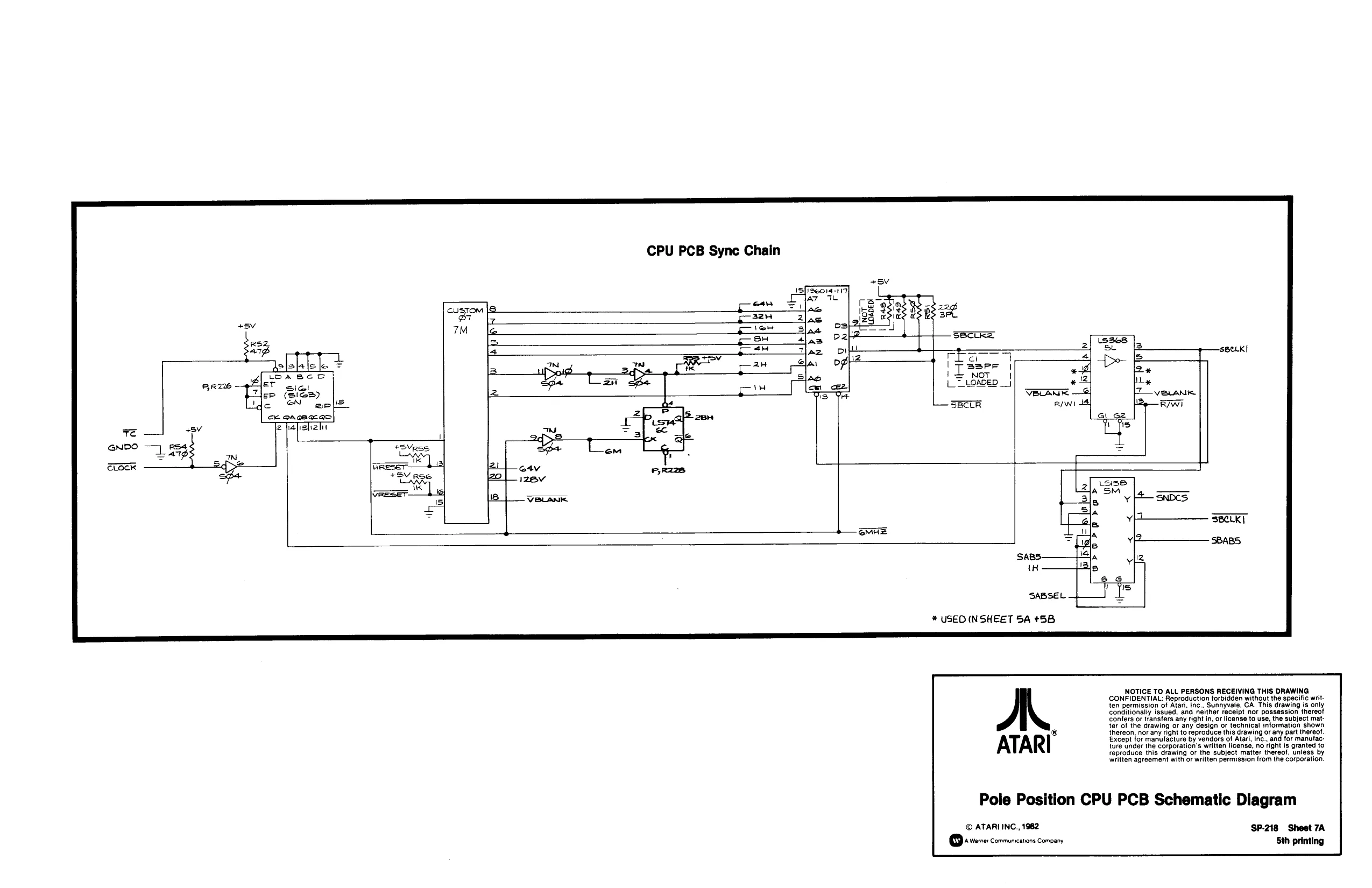
This page is a drawing, shown as the original scan.
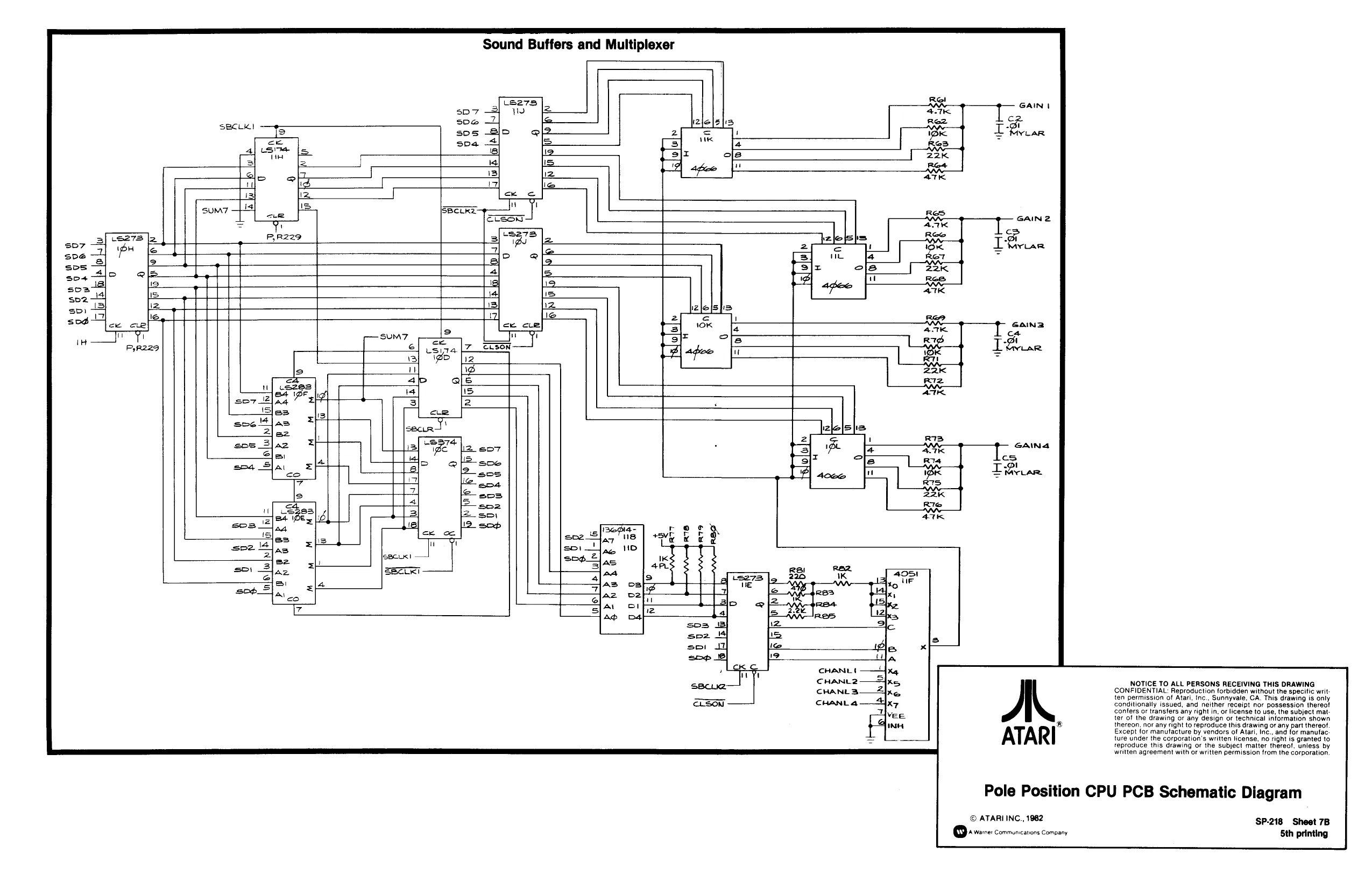
This page is a drawing, shown as the original scan.
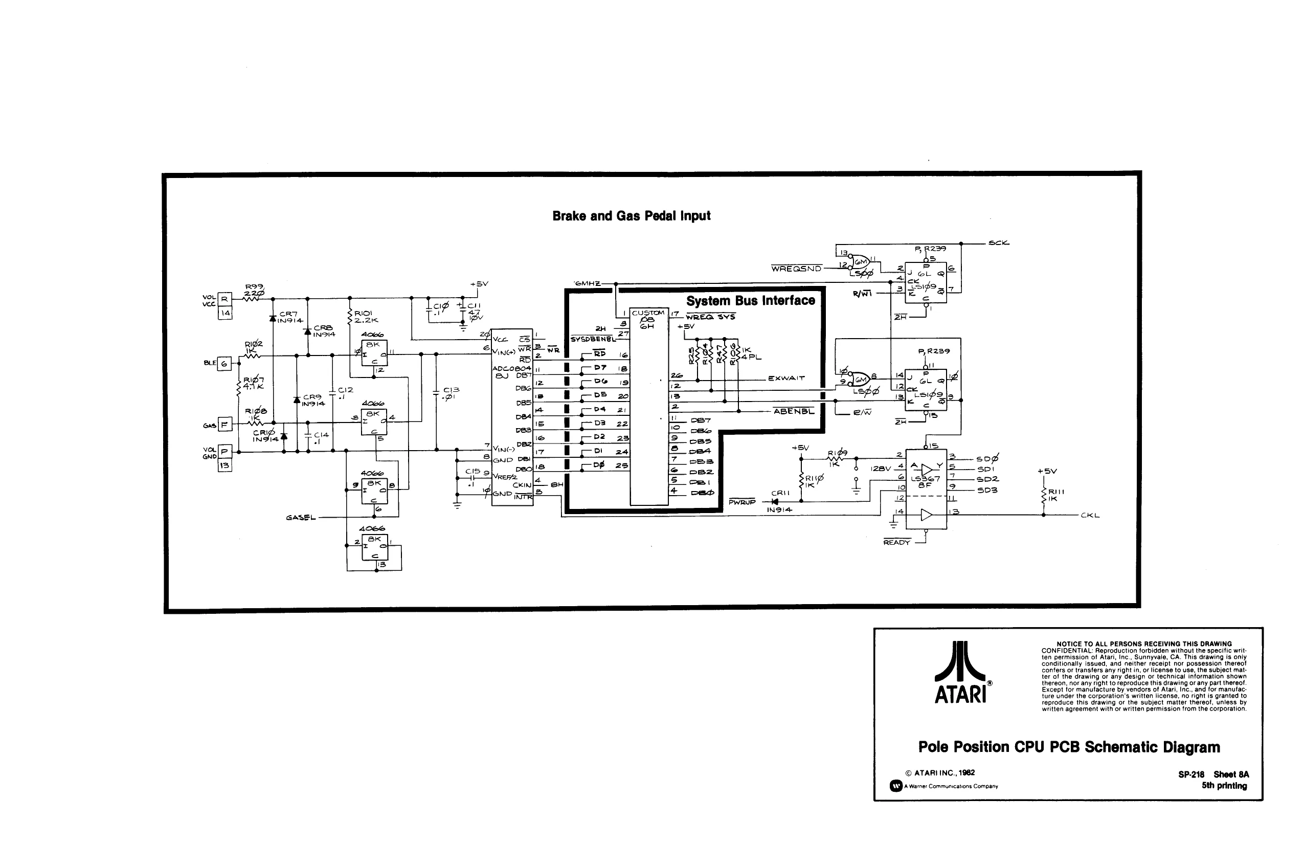
This page is a drawing, shown as the original scan.
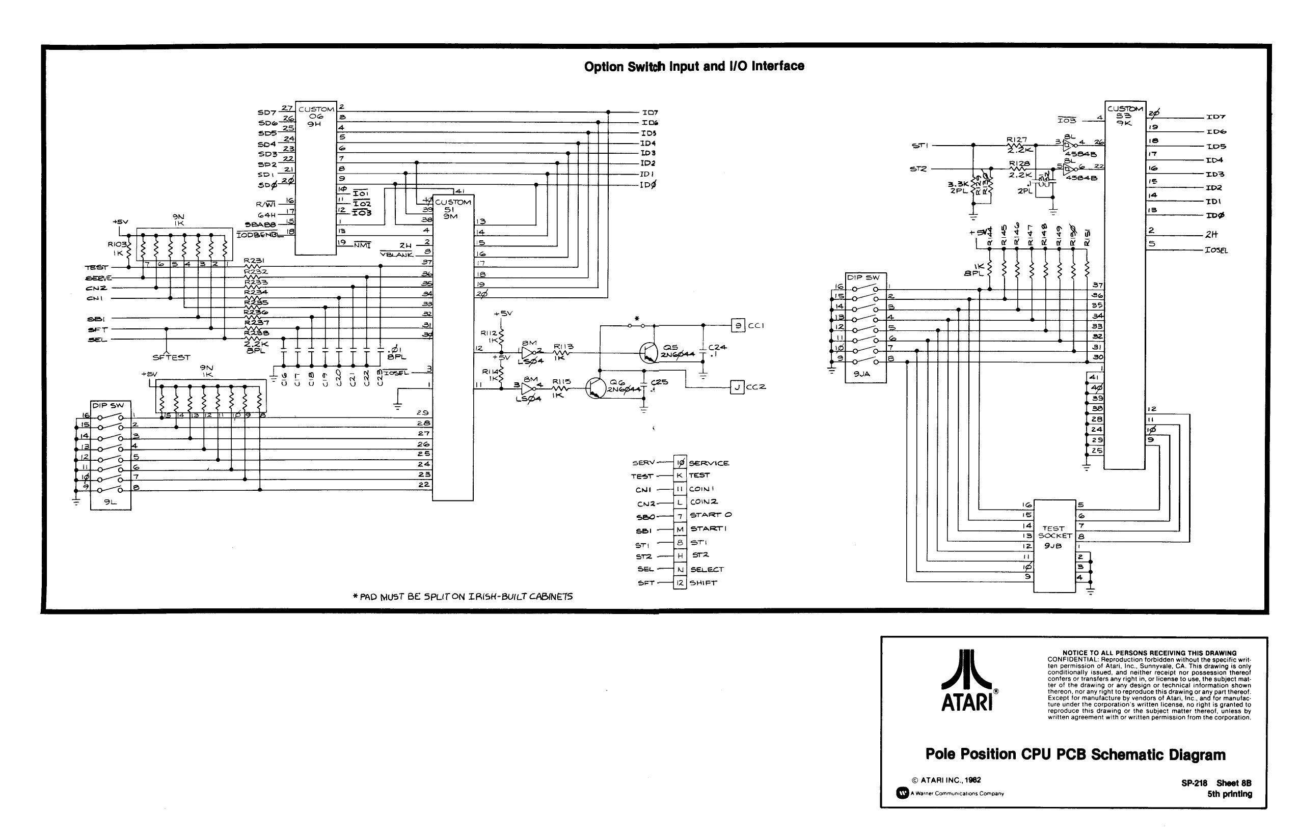
This page is a drawing, shown as the original scan.
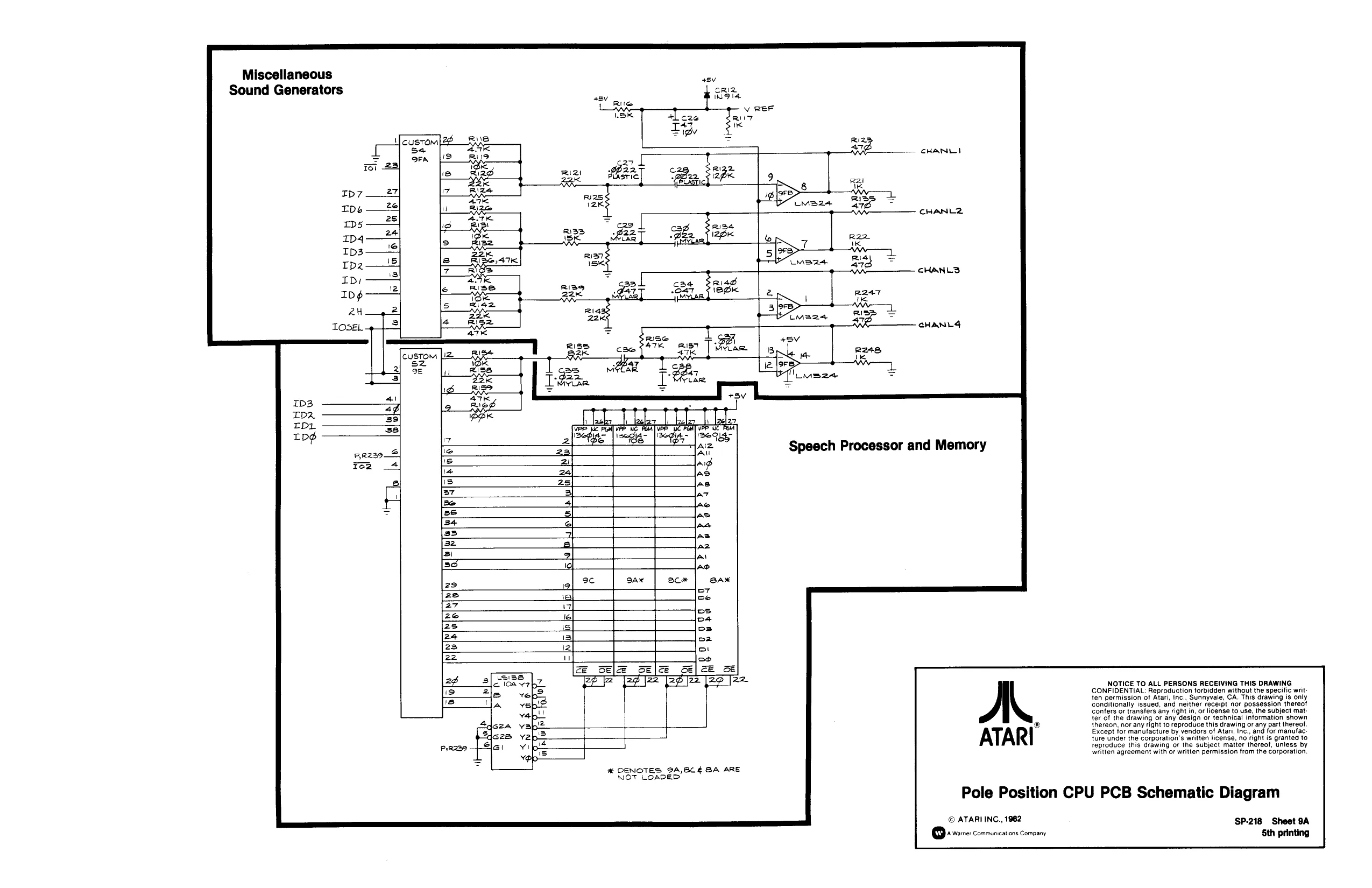
This page is a drawing, shown as the original scan.
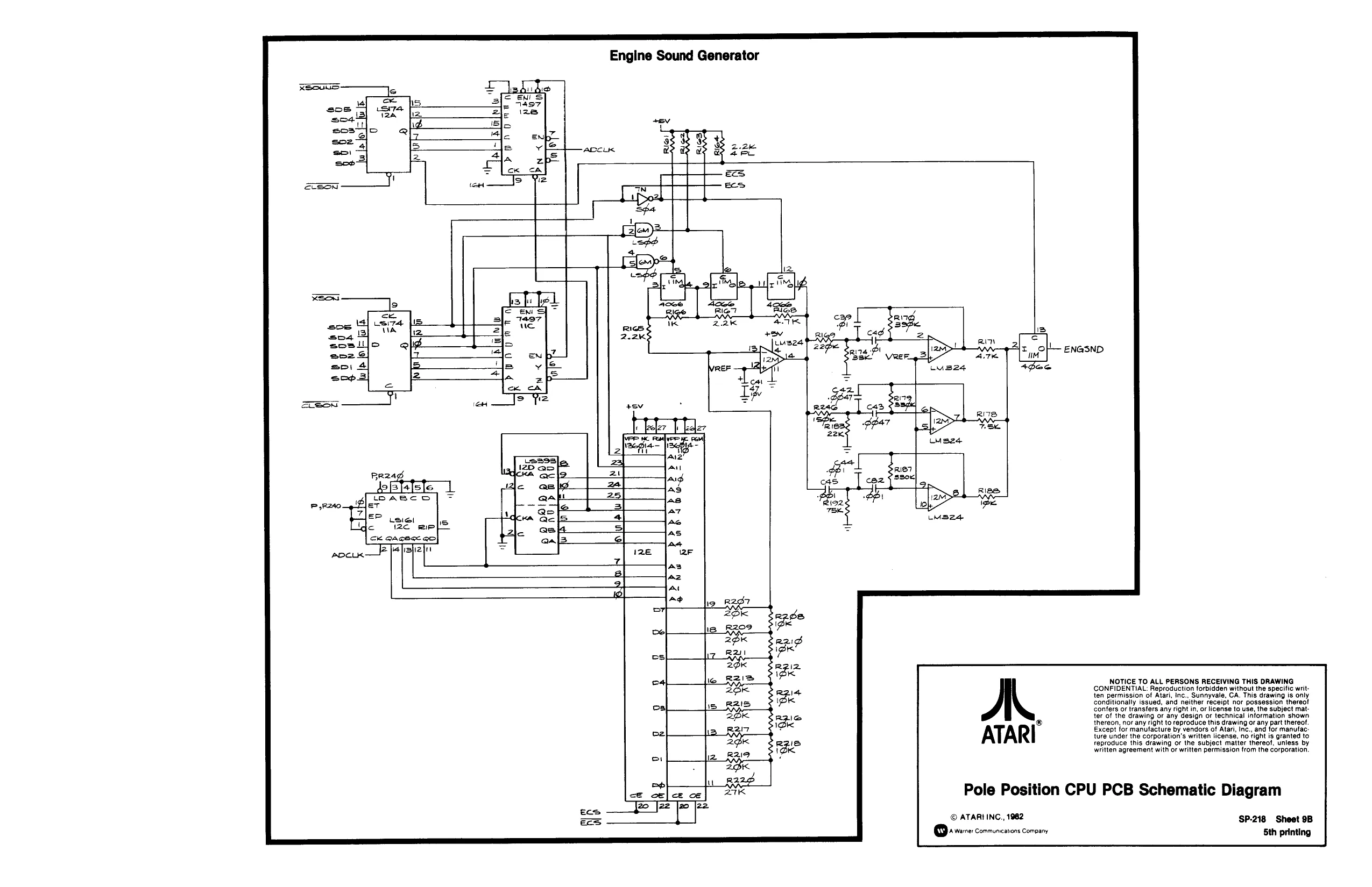
This page is a drawing, shown as the original scan.
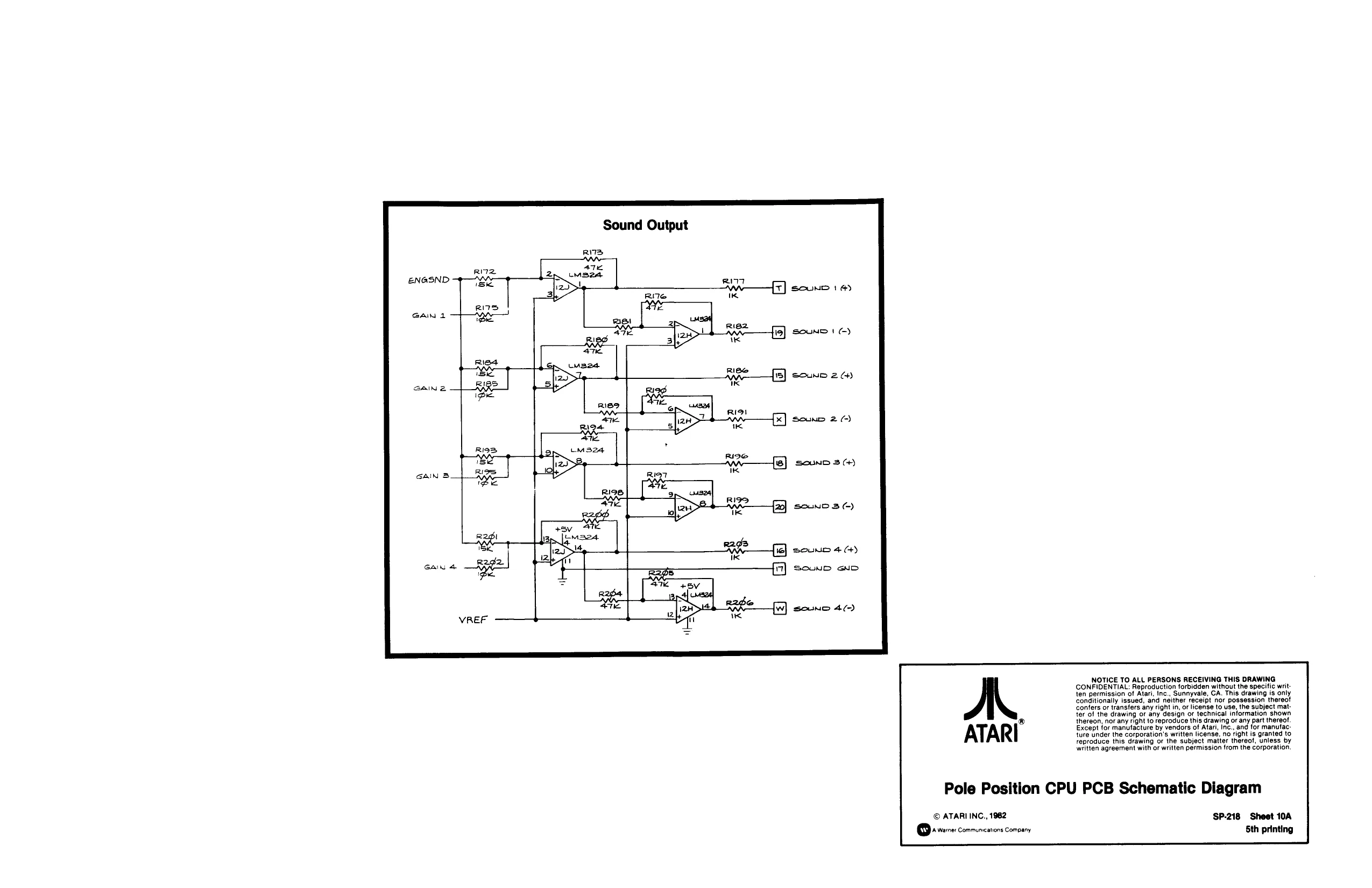
This page is a drawing, shown as the original scan.
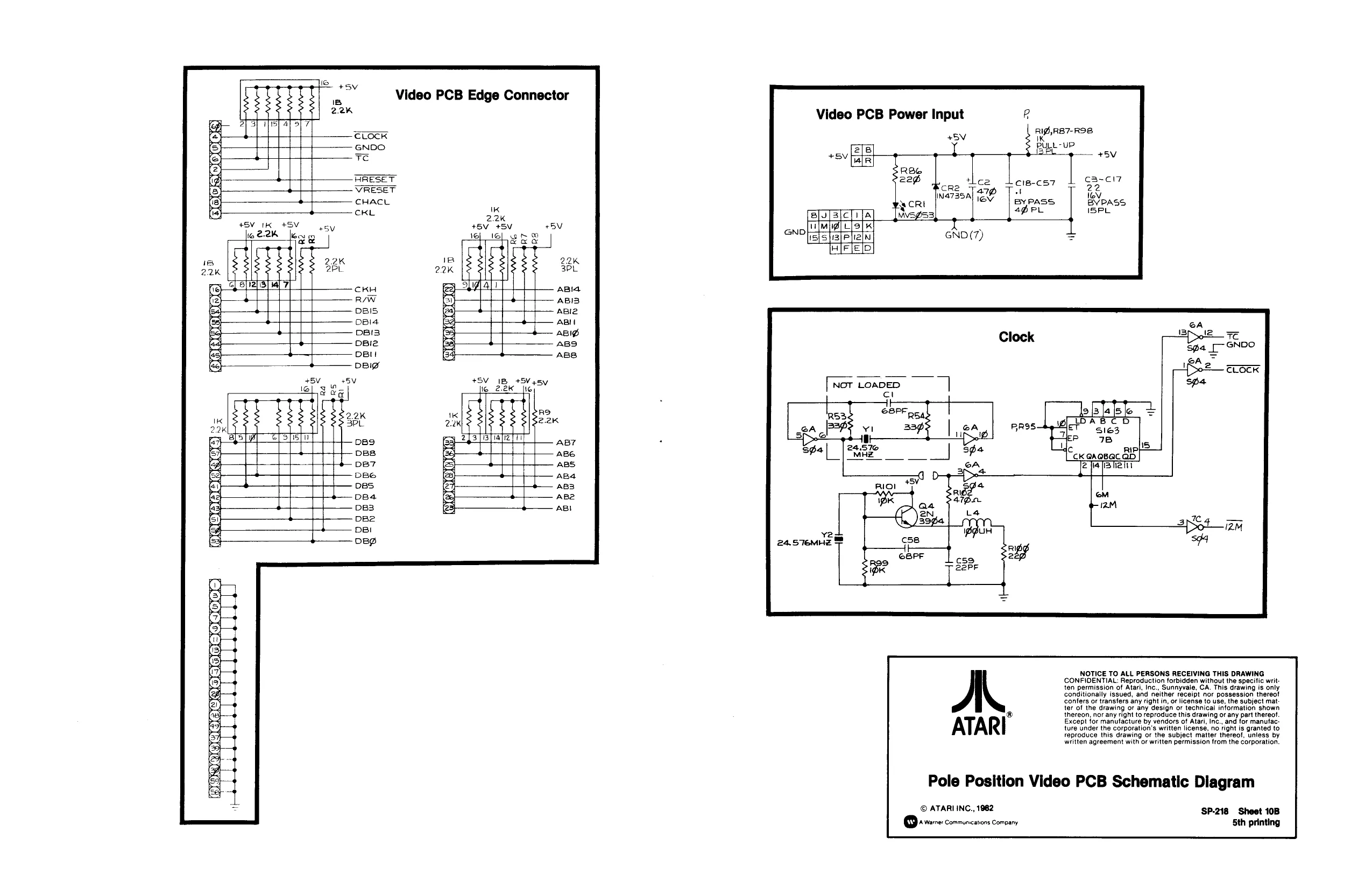
Video PCB Edge Connector
Video PCB Power Input R
RIP,RB7-ROB- +5V Na * GNDO ry Tt ULL -UP babe 2 TC | RBG if [ I RESET 226 thee cie-c57 VRESET cre ESE Warasal 270 Tol CHACL CRI Syrass 1K 4pgPL CKL 22K MVS 53, +5V +5V 16] 16] woe GNO (7)
NOT LOADED
conditionally issued, and neither receipt nor possession thereo! Confers or transfers any right in, or license to use, the subject matter of the drawing or any design or technical information shown ® thereon, nor any right to reproduce this drawing or any part thereof. Except for manufacture by vendors of Atari, Inc., and for manufacture under the corporation's written license, no fight is granted to NOTICE TO ALL PERSONS RECEIVING THIS DRAWING CONFIDENTIAL: Reproduction forbidden without the specific written permission of Atari, Inc., Sunnyvale, CA. This drawing is only
reproduce this drawing or the subject matter thereof, unless by written agreement with or written permission from the corporation.
Pole Position Video PCB Schematic Diagram
© ATARIINC., 1962 SP-218 Sheet 10B Qt verre: communicavons Company Sth printing
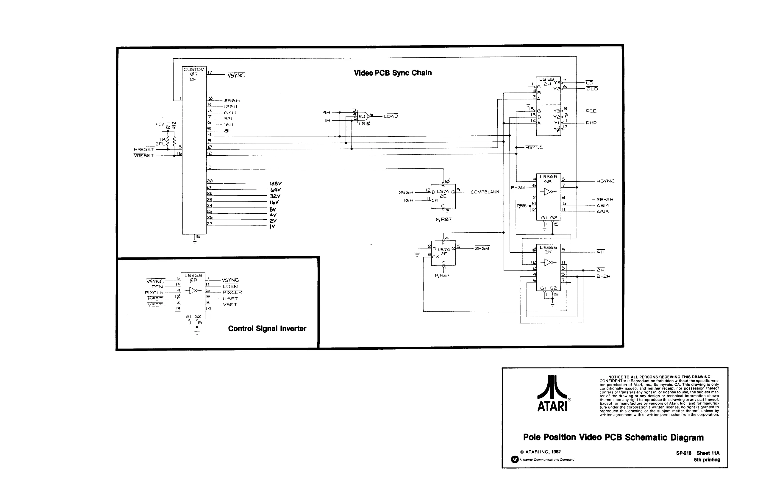
CusTOM BT Veync. Video PCB Sync Chain ar
LSI
VRESET
COMPBLANK
| V5YNC- | S| | ipo | VSYNC |
| LDEN | —2 | (DEN | |
| PIXCLK | 4p | PIRKCLR |
aseT — 2 HSeT
| Veer | 2 | vseT |
Gl G2
KP Control Signal Inverter
NOTICE TO ALL PERSONS RECEIVING THIS DRAWING CONFIDENTIAL: Reproduction forbidden without the specific writ ten permission of Atari, Inc., Sunnyvale, CA. This drawing is only conditionally issued, and neither receipt nor possession thereof confers or transfers any right in, or license to use, the subject mat ter of the drawing or any design oF technical information shown 8 thereon, nor any right to reproduce this drawing or any part thereof.
Except for manufacture by vendors of Atari, Inc., and for manufac:
ture under the corporation's written license, no right is granted to reproduce this drawing or the subject matter thereof, unless by written agreement with or written permission from the corporation.
Pole Position Video PCB Schematic Diagram
© ATARI INC., 1982 ‘SP-218 Sheet 11A > Ware: conmneations Company 5th printing
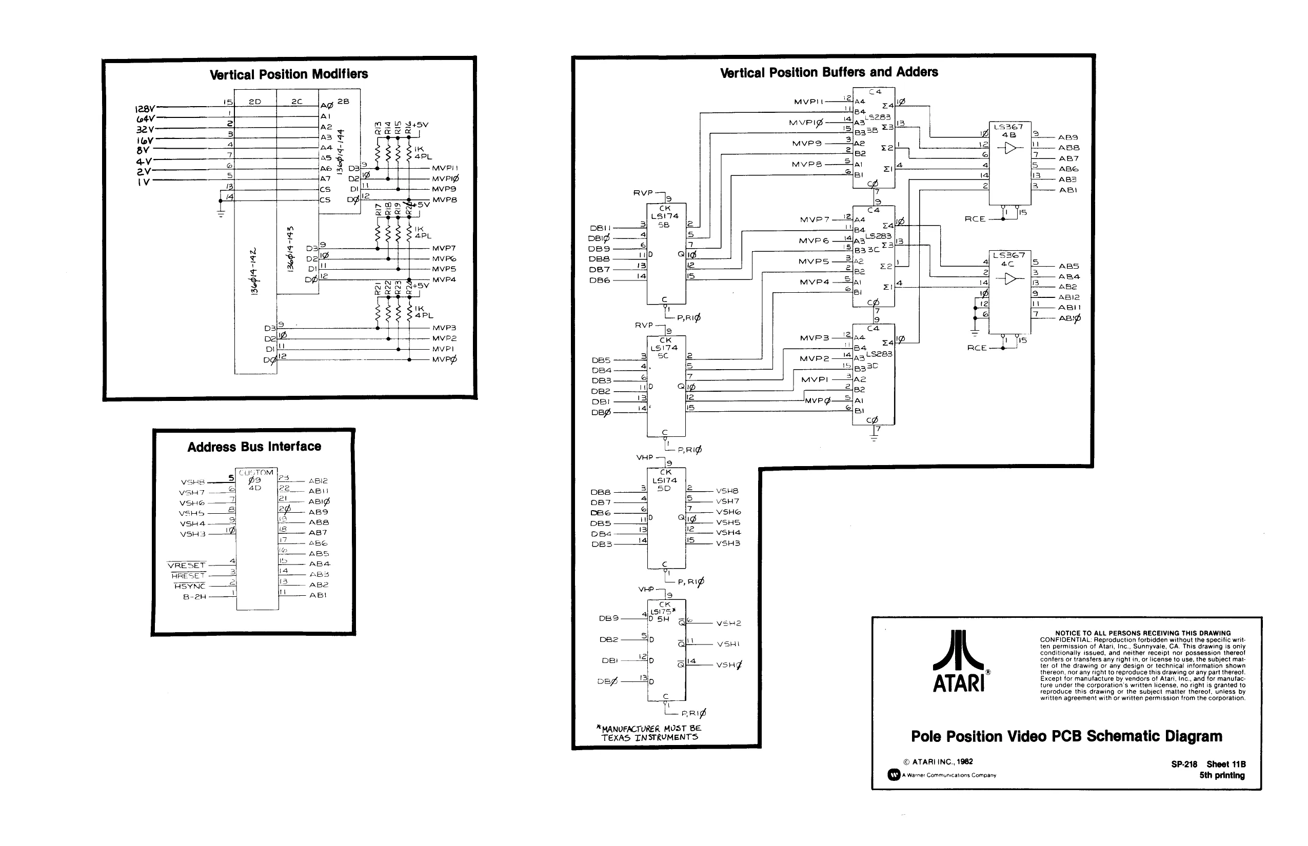
Vertical Position Buffers and Adders
Vertical Position Modifiers
ca
| | | 2D | 2c | dag 28 | Mvp. | —2 ae | zal! |
At ta] -S263
| 2 | laces | MvPIg-— es AS | sal/3 | Lase7 | ||||
| $ | + | pase | Zi | > | ||||
| ast | = | 3 | a5 | ABS | ||||
| 4 | aay | Mw | aes | eet! | 12} | > | | | ase |
| 2. | 15% | ABT |
s
| A | wa pal | MVPS | ai | silt | al | Bane |
| S | ee | iB | ta] | IB | ABs |
Ics Ss Ho,
1314-142
Address Bus Interface
COGTOM |, Ey 4D le ()
fSily jo jo
VRESET RESET SYNE B-2H
NOTICE TO ALL PERSONS RECEIVING THIS DRAWING CONFIDENTIAL: Reproduction forbidden without the specific written permission of Atari, Inc., Sunnyvale, CA. This drawing is only conditionally issued, and neither receipt nor possession thereo! confers or transfers any right in, or license to use, the subject matter of the drawing or any design or technical information shown ® thereon, nor any right to reproduce this drawing or any part thereot Except for manufacture by vendors of Atari, Inc., and for manufacture under the corporation's written license, no right is granted to feproduce this drawing or the subject matter thereof. uniess by written agreement with or written permission from the corporation.
sri
- MANUFACTURER MUST BE TEXAS INSTRUMENTS
Pole Position Video PCB Schematic Diagram
© ATARI ING., 1982 SP-218 Sheet 11B vere: communeations Company Sth printing
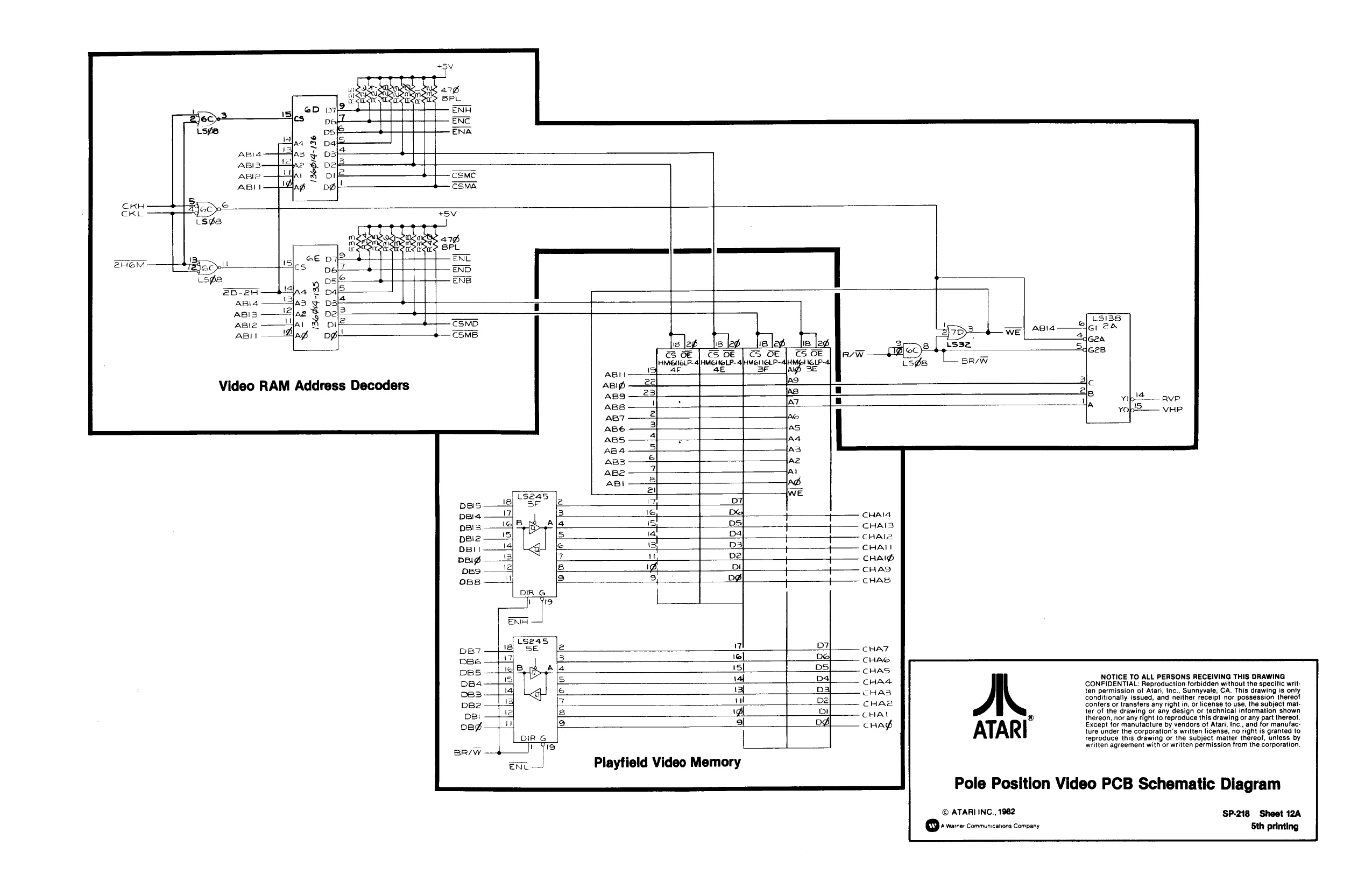
IAB x D: ABIS jaz & pal ABI War & oi =o fw [BOIS
ABII 1D Ag og
Video RAM Address Decoders
DB7 DBE DBS DB4 DBS pez DBI oBg
BR/W —4¢—_ OD 8 os wy
2 ind
| 3 | 16] | bel |
| [4 | 15) | DS |
| IS | val | ba |
| le | 131 | [ee |
| 7 | m1 | oe] |
| iB | ial | DI |
mn 2 ET DIR G
ENC
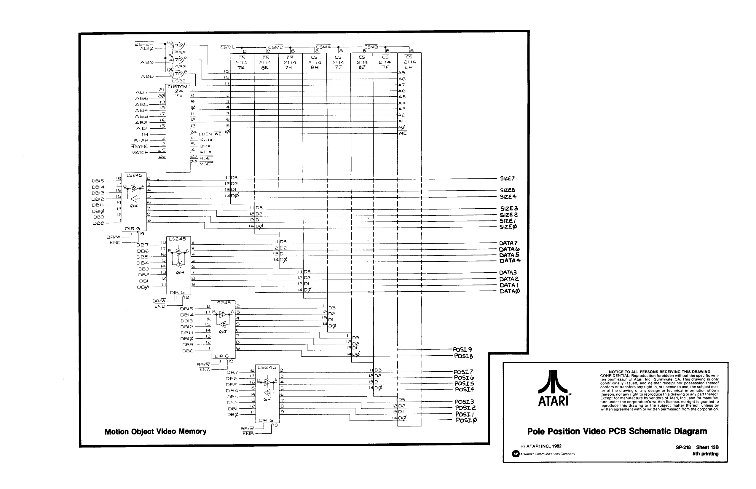
Playfield Video Memory
CHAT CHAS CHAS CHAS CHAS cHae CHA cHag NOTICE TO ALL PERSONS RECEIVING THIS DRAWING CONFIDENTIAL: Reproduction forbidden without the specific writ: ten permission of Atari, Inc., Sunnyvale, CA. This drawing is only conditionally issued, and neither receipt nor possession thereot confers or transfers any right in, or license to use, the subject matter of the drawing or any design oF technical information shown ® thereon, nor any right to reproduce this drawing or any part thereof. Except for manufacture by vendors of Atari, Inc., and for manufac: ture under the corporation's written license, no right is granted to reproduce this drawing or the subject matter thereof, unless by written agreement with or written permission from the corporation.
Pole Position Video PCB Schematic Diagram
© ATARI INC., 1982 ‘SP-218 Sheet 12A > are: communications Company 5th printing
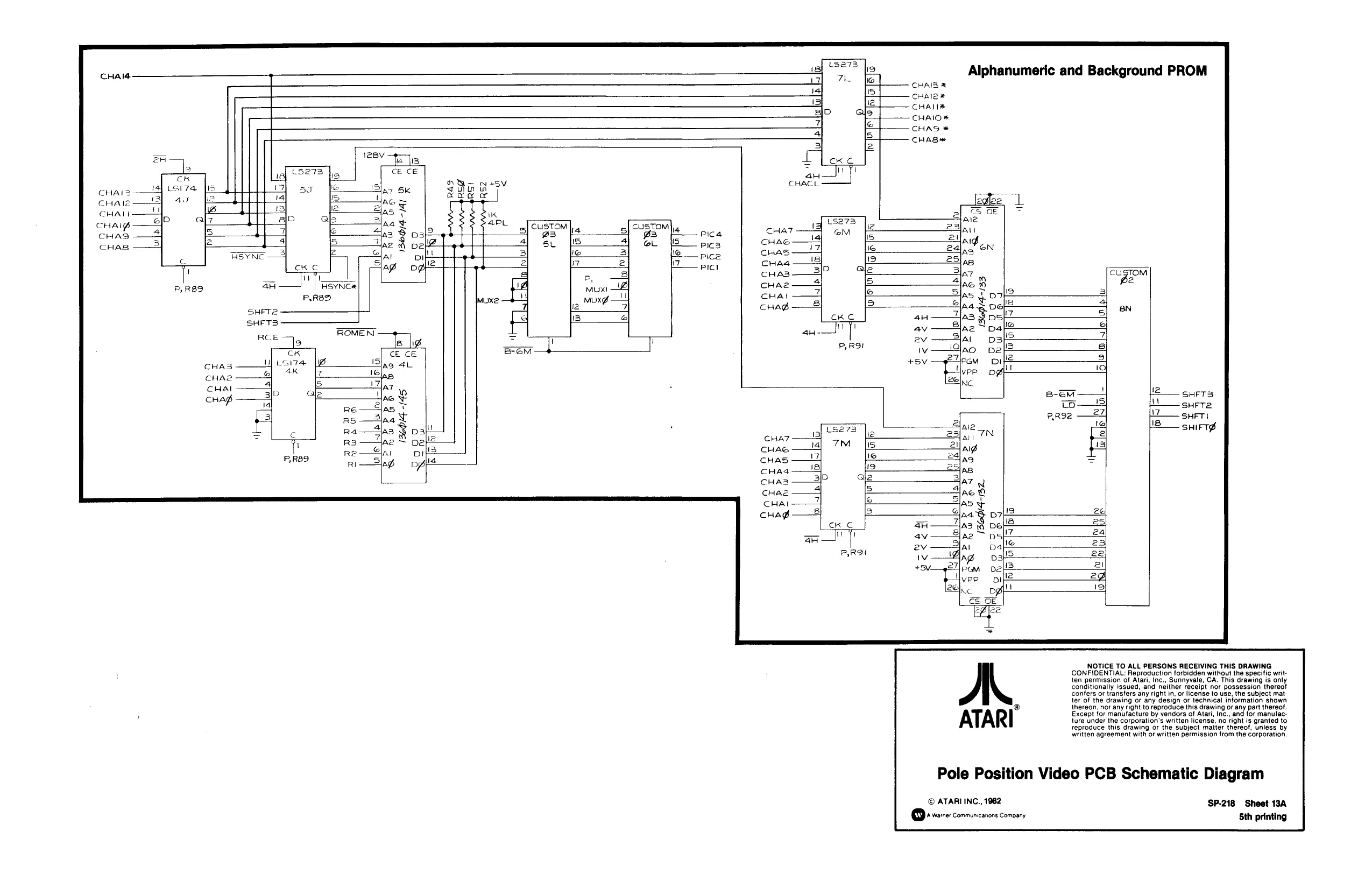
This page is a drawing, shown as the original scan.
This page is a drawing, shown as the original scan.
This page is a drawing, shown as the original scan.
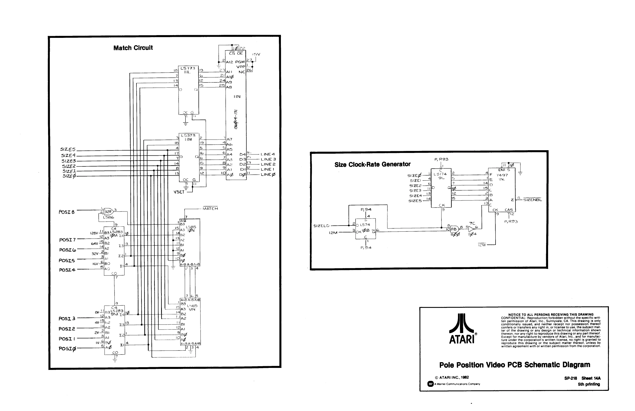
Match Circuit
Size Clock-Rate Generator
sized SIZEI size sizes size4 SIZES SiENBL 1S [uo bon I lon for fas |
F &
SIZELD
12M
logs In<B A-B/-8] 2B |
7 Je |S ARBAB AB) B? oes, IAs ON Se2
El NOTICE TO ALL PERSONS RECEIVING THIS DRAWING
a2 CONFIDENTIAL: Reproduction forbidden without the specific writ: BI ten permission of Atari, Inc., Sunnyvale, CA. This drawing is only
® conditionally issued, and neither receipt nor possession thereof At Conters or transters any right in, or license to use, the subject matfer of the drawing or any design or technical information shown Bd thereon, nor any right to reproduce this drawing or any part thereof. Zé Except for manufacture by vendors of Atari, Inc., for manufac- [As ture under the corporation's written license, no right is granted to IA<B A=B AB} reproduce this drawing or the subject matter thereof, unless by ‘written agreement with or written permission from the corporation.
Pole Position Video PCB Schematic Diagram
© ATARI INC., 1982 SP-218 Sheet 144 > verre: communcations Company 5th printing
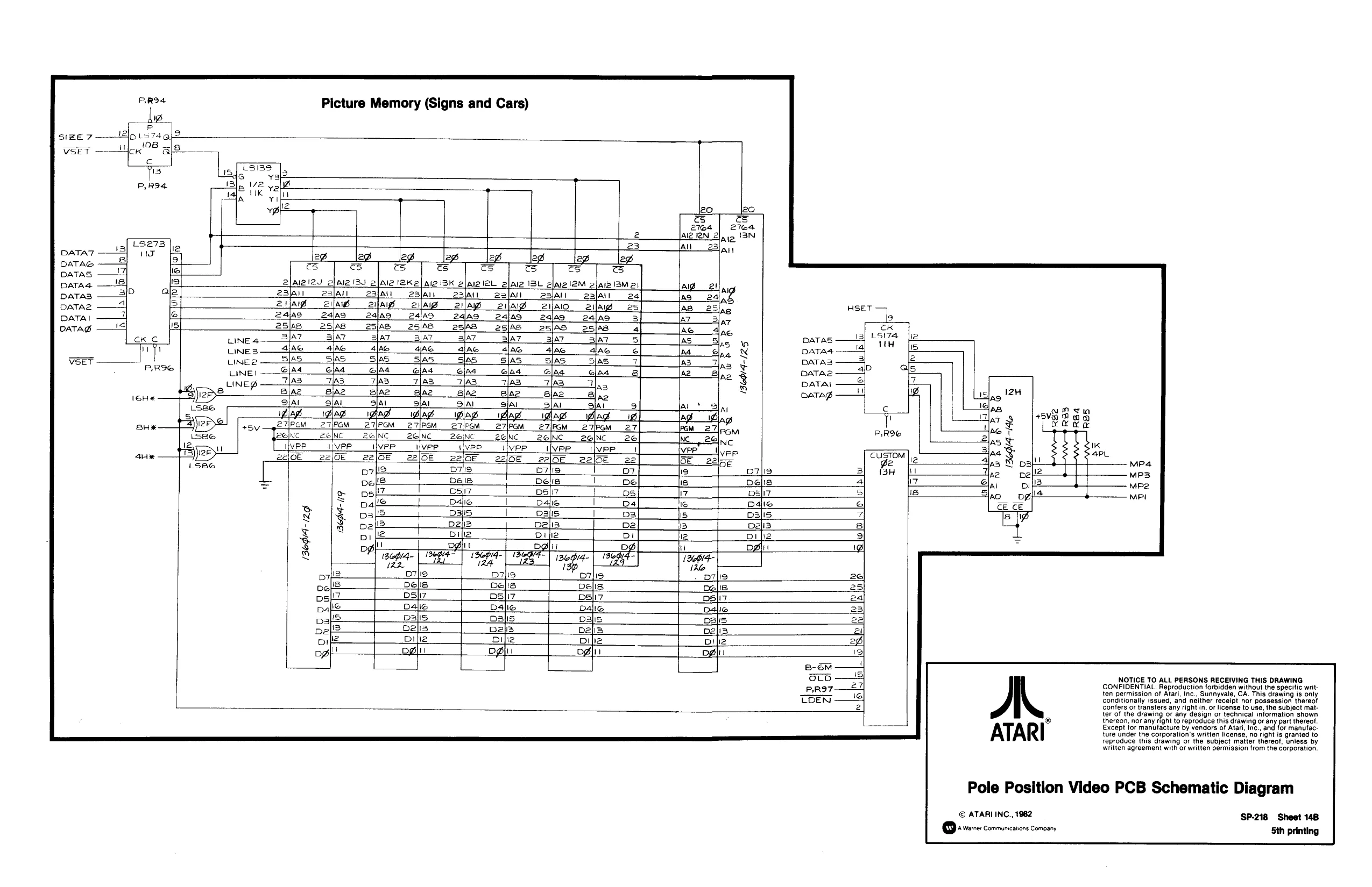
Picture Memory (Signs and Cars)
leg
iz BL e| lai2 2M
23lan 2AIO In tro i Jo
24] w 25) Jo fue Jw
lw Joo Jos Jor Ju Jon BR BBRGB 1BObl4-125, a lal
la2 0 foo {a Jor urn fw Ko Joo IN Jo fon fs.
AL a
2lNC tWeP 4PL 22\0E 22 Mp4 p7fio MP3 Delis Jun 16 Jou [ds [w fry |~ [5 16 |e
MP2 bs li7, MPI Bale 3s Delis +444) BPA Dif $8 [uo Joo [fo fords ws
130$4- izg Dili Te
A.
ATARI
NOTICE TO ALL PERSONS RECEIVING THIS DRAWING CONFIDENTIAL: Reproduction forbidden without the specitic writ ten permission of Atari, Inc., Sunnyvale, CA. This drawing is only conditionally issued, and neither receipt nor possession thereot conters or transfers any right in, or license to use, the subject matter of the drawing or any design or technical information shown thereon, nor any right to reproduce this drawing or any part thereof. Except for manufacture by vendors of Atari, Inc., and for manufac: ture under the corporation’s written license, no right is granted to reproduce this drawing or the subject matter thereof, unless by written agreement with or written permission from the corporation.
Pole Position Video PCB Schematic Diagram
© ATARI INC., 1962 vere conmuncatons Company SP.218 Sheet 148 5th printing
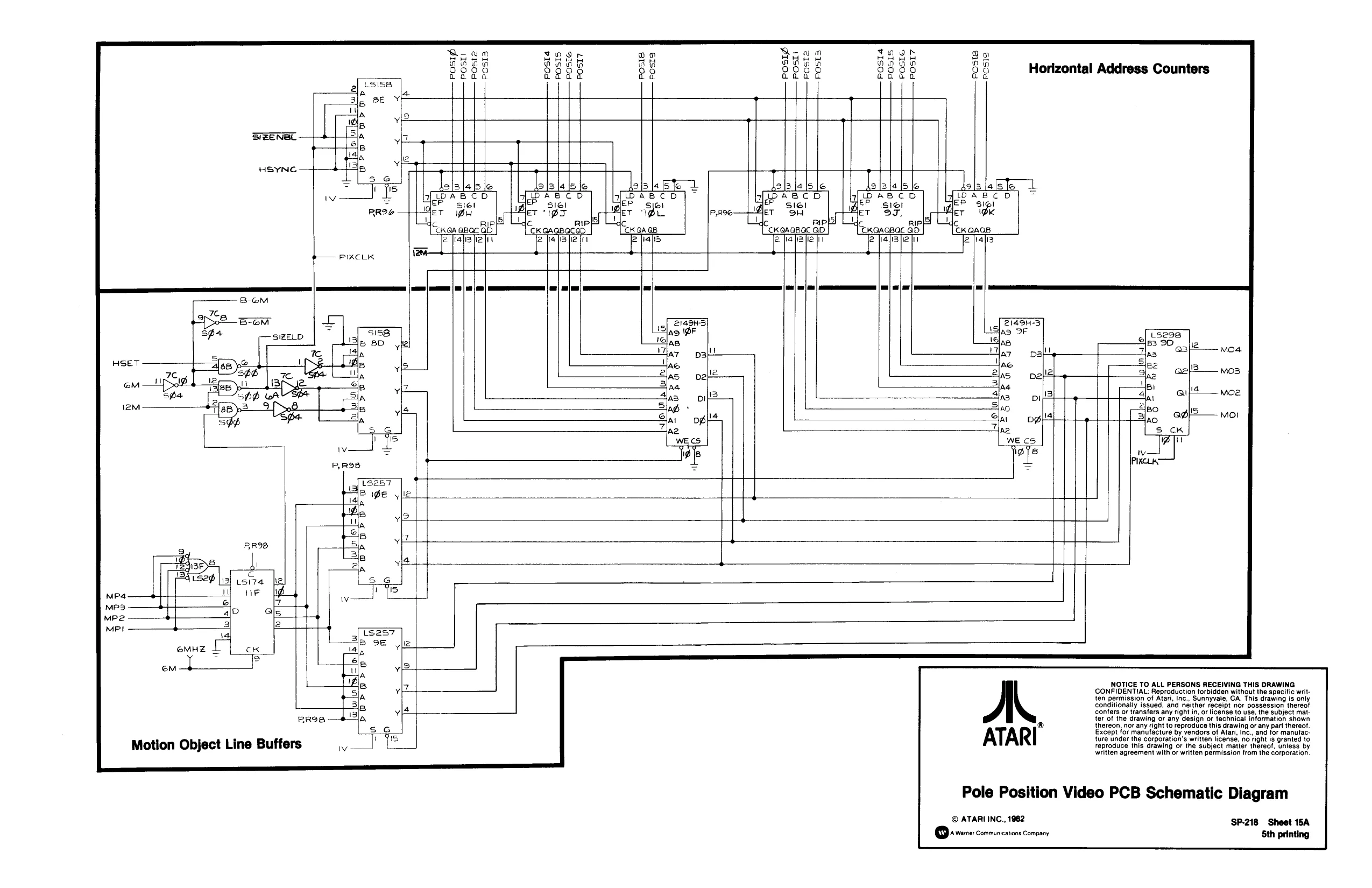
HSET
12M Sate Bese HEE gag aiac eeee
3\6 nN iB STENBC = + B a HSYNG +35 Posi. PoSsIa PosIg POSI! post2 POSLS POSI4 POSIS: POSIe
POSI7
Posts Posia
B-oM 7C, 208 B-EM Spe SIZELD
POrOPuUP S158 Horizontal Address Counters
| E1455] | ef | 24583 | ||||
| 2a iF | : | Jaa DF | @| LS298 | |||
| AB | AB | 183 2D | hie | |||
| a7 | pal! | a7 | patty | zs | & | Mos: |
i ;
| 6 | Ao | lez | 13 |
Mo3
| Eas | vats | 2s | pal! | | | ae | |
| mila | rind | ae! | ail'4¢ | moe | ||
| Sina | pit | Spas | py | Stat | ||
| Shp | + | AO | Spo | 1S | ||
| Siar | gli | Sly | gil | ao | 6) | mor |
| Zip | Tne | Ss | cK |
Motion Object Line Buffers
iw o ES
E nS roOror
A © D s257
AL ATARI
© ATARIINC., 1962 vee conmncains Conny
Pole Position Video PCB Schematic Diagram
NOTICE TO ALL PERSONS RECEIVING THIS DRAWING
CONFIDENTIAL: Reproduction forbidden without the specitic writ thereon, nor any right to reproduce this drawing of any part thereof
ten permission of Atari, Inc., Sunnyvale, CA. This drawing is only Conditionally issued, and neither receipt nor possession thereot confers or transfers any right in, or license to use, the subject matter of the drawing or any design or technical intormation shown thereon, nor any right to reproduce this drawing of any part thereof. Except for manufacture by vendors of Atari, Inc., and for manufacture under the corporation’s written license, no right is granted to reproduce this drawing or the subject matter thereof, unless by written agreement with or written permission from the corporation.
SP-218 Sheet 15A Sth printing
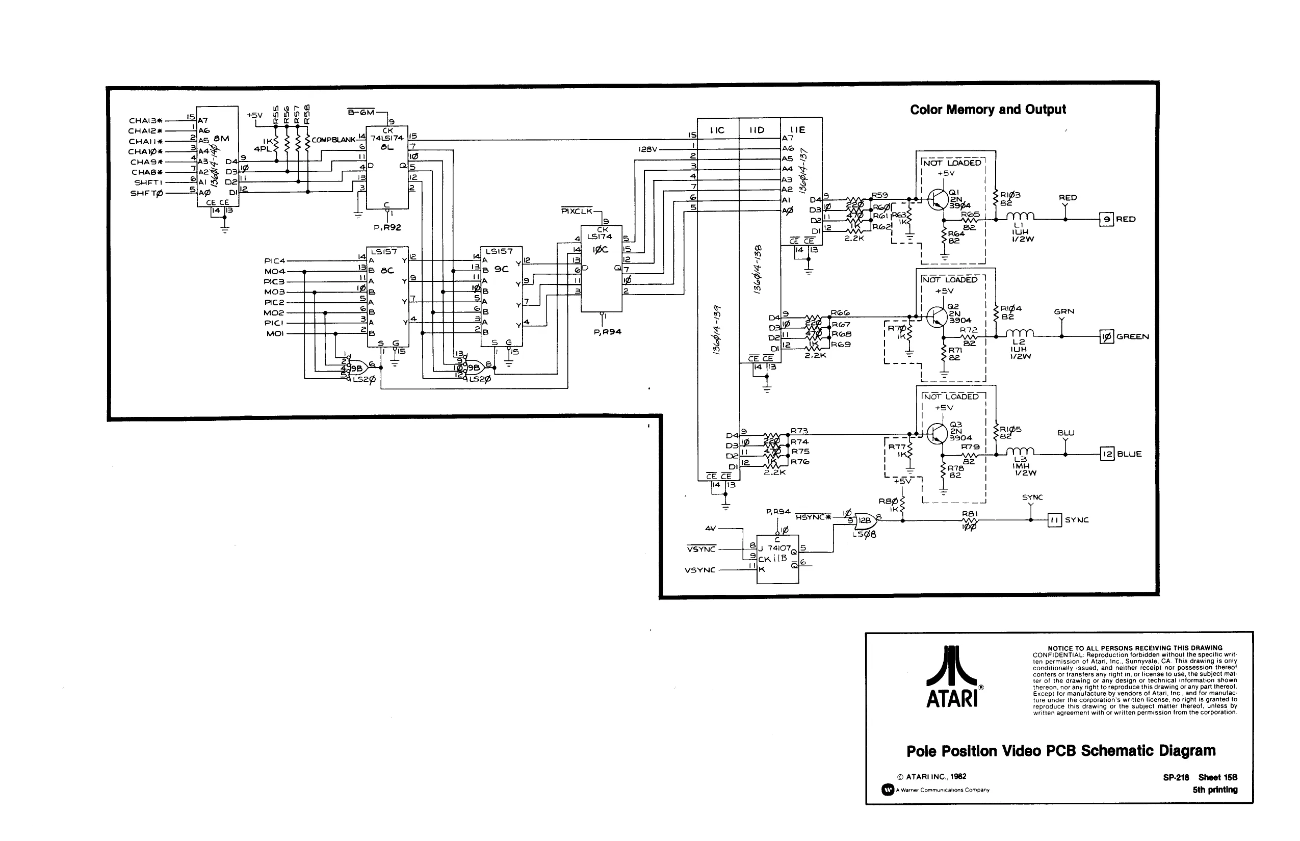
CHAI3® cHalex CHAI ——S CHAID* CHAS CHABE SHFT! SHFTD
Color Memory and Output
= |
& ° Eq oh
-/4 oR Jur Jor Ju | Jw fro
ut [wy | fw [ro
DrPnrorgr
conters or transfers any right in, or license to use, the subject mat: ter of the drawing or any design or technical information shown
® thereon, nor any right to reproduce this drawing or any part thereof,
Except for manufacture by vendors of Atari, Inc., and for manufac: ture under the corporation's written license, no right is granted to reproduce this drawing or the subject matter thereof, unless by written agreement with or written permission from the corporation. NOTICE TO ALL PERSONS RECEIVING THIS DRAWING CONFIDENTIAL: Reproduction forbidden without the specific writ ten permission of Atari, inc., Sunnyvale, CA. This drawing is only conditionally issued, and neither receipt nor possession thereof
Pole Position Video PCB Schematic Diagram
© ATARI INC., 1982 ‘SP-218 Sheet 15B + warre:communcatons Company Sth printing
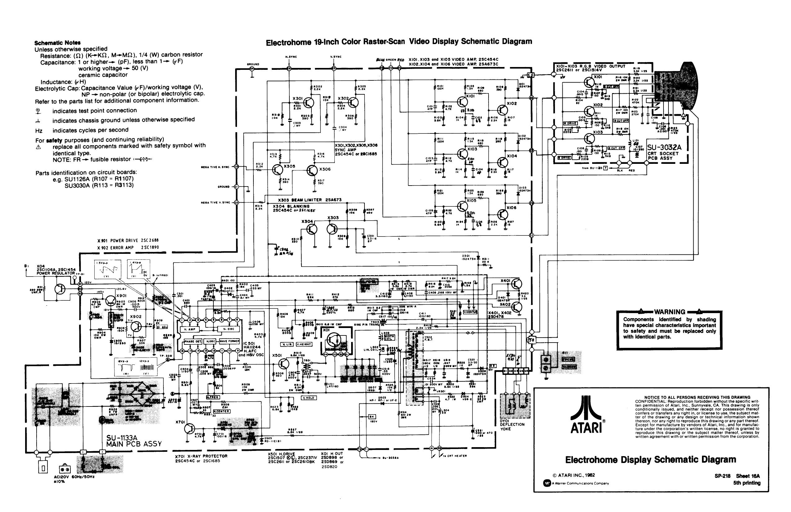
Schematic Notes Electrohome 19-Inch Color Raster-Scan Video Display Schematic Diagram Unless otherwise specified Resistance: (2) (KKQ, M--MQ@), 1/4 (W) carbon resistor Capacitance: 1 or higher-> (pF), less than 1—> (yF) working voltage -» 50 (V) ceramic capacitor Inductance: (# H) ; Electrolytic Cap: Capacitance Value (/ F)/working voltage (V), NP -= non-polar (or bipolar) electrolytic cap. Refer to the parts list for additional component information.
2 indicates test point connection oh indicates chassis ground unless otherwise specified Hz indicates cycles per second wene wane Biug oncen Rep XIO1.XI03 and X08 VIDEO AMR 25C454C X102.xI04 and XI06 VIDEO AMR. 2SA673C ‘enouno XIOl~XI03 R.G.B VIOEO OUTPUT 2SC26It or 28CI5I4V.
For safety purposes (and continuing reliability) ; a replace all components marked with safety symbol with 052A, identical type. SU-3052A
Maen TIVE v. SYNE X304 BLANKING 23C484C oF 26ci6es
nee Lner Tk gis!
X901 POWER DRIVE 2SC 2688 X 902 ERROR AMP —2SC1890
Vave0 x04 28cii06a, 28c1456 PAP Yh REGULA)
‘WARNING Components Identified by shading have special characteristics important to safety and must be replaced only with identical parts.
NOTICE TO ALL PERSONS RECEIVING THIS DRAWING CONFIDENTIAL: Reproduction forbidden without the specitic written permission of Atari, Inc., Sunnyvale, CA. This drawing is only conditionally issued, and neither receipt nor possession thereof confers or transfers any right in, or license to use, the subject matter of the drawing or any design or technical information shown ® thereon, nor any right to reproduce this drawing or any part thereof. Except for manufacture by vendors of Atari, Inc., and for manufac: ture under the corporation's written license, no right is granted to reproduce this drawing or the subject matter thereof, unless by written agreement with or written permission from the corporation.
ce X701 X-RAY PROTECTOR X501_H.ORIV| XO HOUT le tee 2SCa54C or 25ci685 caer C'sscesoae 2svec0 wenense Electrohome Display Schematic Diagram 2S0820
ACIZOV 6OH2/SOHE © ATARI INC., 1962 ‘SP-218 Sheet 16A 210% QA waive: communcations Company 5th printing
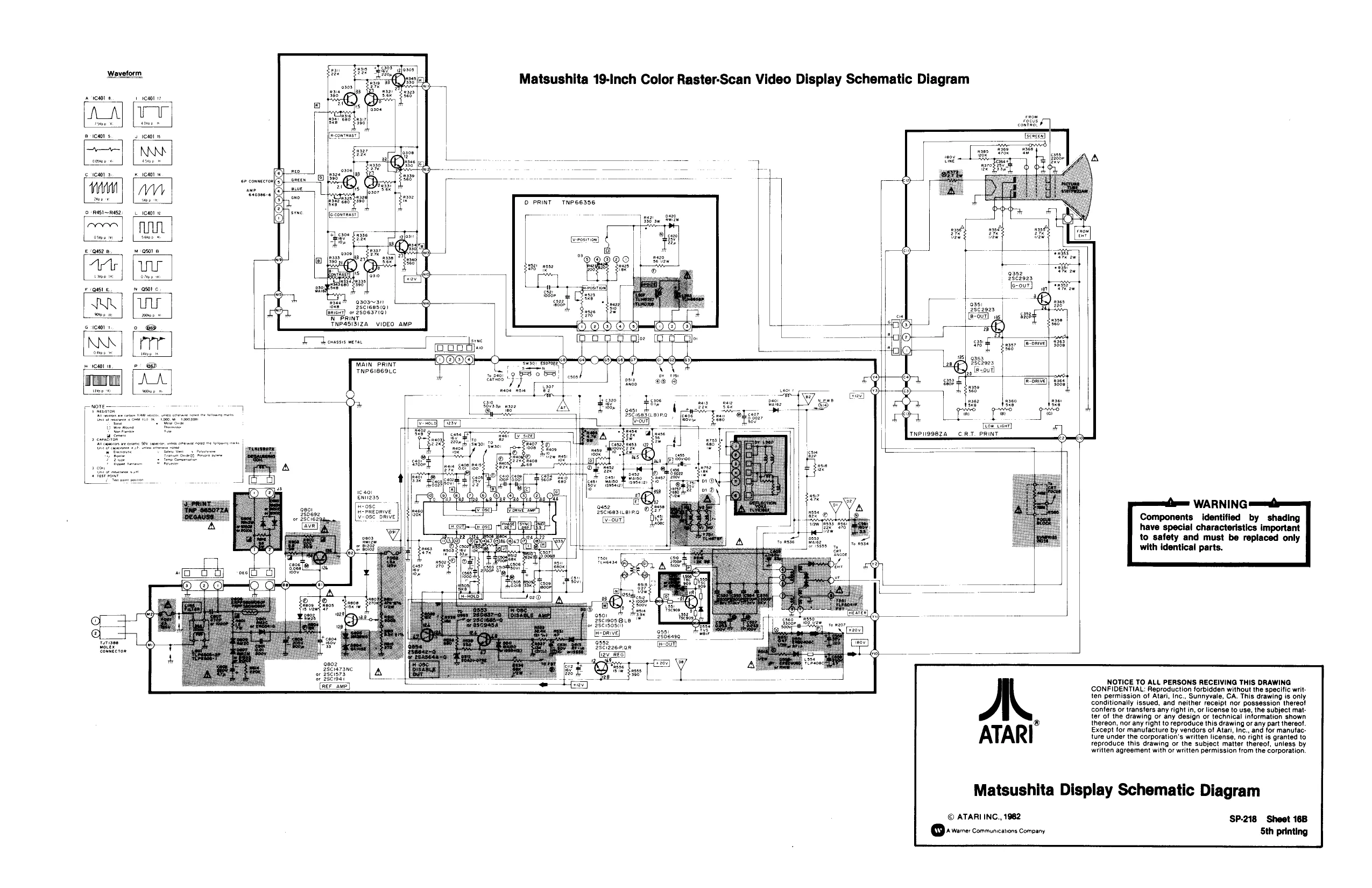
a 1001 & 1 reaot SA
91040 5 41101
~—
< 1cm 2 Kk 1ca01
O:RUSI~ RAS? ICAO ww
5 0082 @
Foust €
Ferrin)
ican a Matsushita 19-Inch Color Raster-Scan Video Display Schematic Diagram
conte |
[sense]
N PRINT TNP4SI3IZA_VIDEO_AMP
Fthenassis mera \ A
A
-— wT
al ee
B-our] IT dae w -
a sayy Bpave)) $355
fy F-ouTl
CRT_PRINT,
NOTICE TO ALL PERSONS RECEIVING THIS DRAWING CONFIDENTIAL: Reproduction forbidden without the specific written permission of Atari, Inc., Sunnyvale, CA. This drawing is only conditionally issued, and neither receipt nor possession thereof confers or transfers any right in, or license to use, the subject matter of the drawing or any design or technical information shown e thereon, nor any right to reproduce this drawing or any part thereof. Except for manufacture by vendors of Atari, Inc., and for manufac: ture under the corporation's written license, no right is granted to Feproduce this drawing or the subject matter thereof, unless by written agreement with or written permission from the corporation.
Matsushita Display Schematic Diagram
© ATARI INC., 1962 SP-218 Sheet 16B Qt vere: conmuncaions Company Sth printing