Space Duel SP-181 1st Printing
Space Duel (version 2) (Atari, 1980) · Schematic Package · 20 pages · 66 sections · original scan
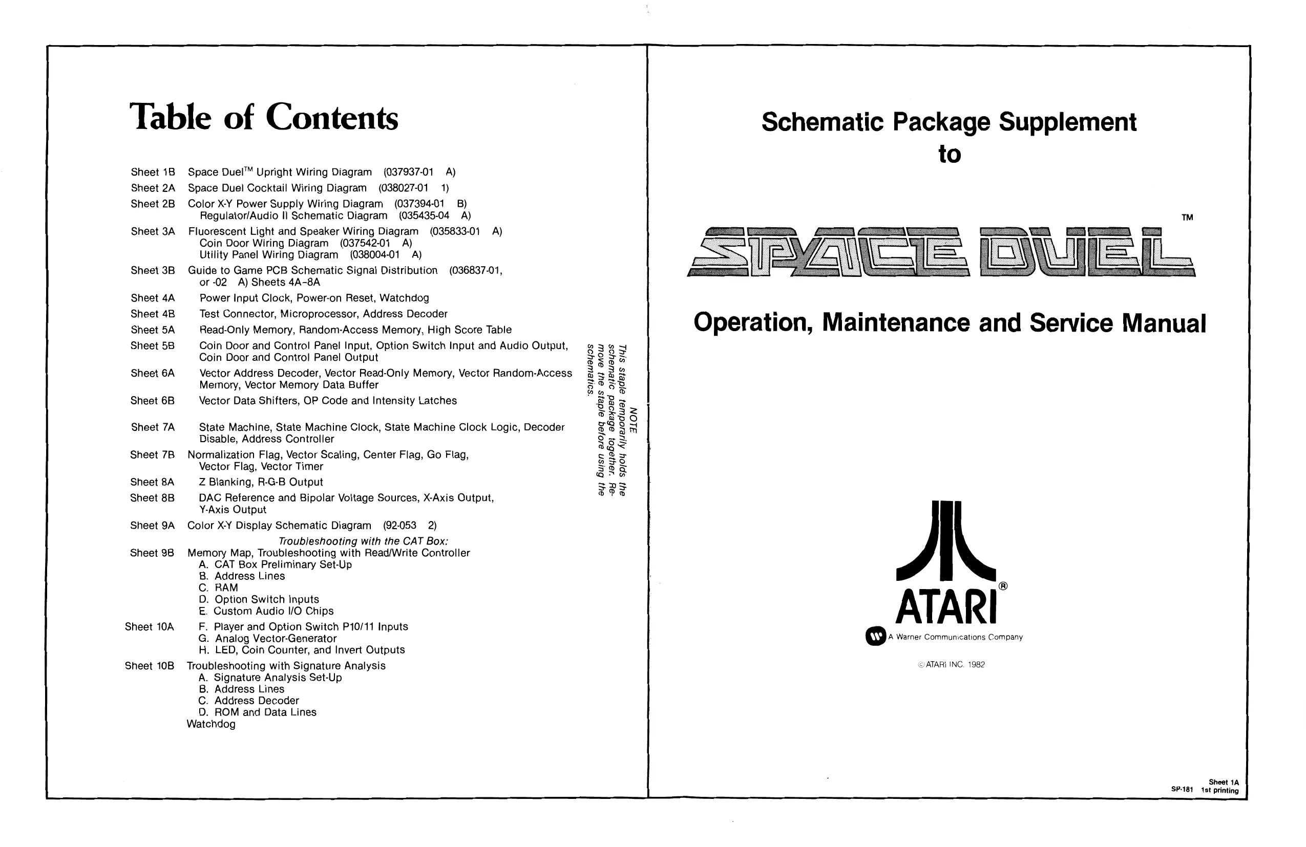
Table of Contents Schematic Package Supplement
to Sheet 1B Space Duel™ Upright Wiring Diagram (037937-01 A) Sheet 2A Space Duel Cocktail Wiring Diagram (038027-01 1) Sheet 2B Color X-Y Power Supply Wiring Diagram (037394-01 B) Regulator/Audio Il Schematic Diagram (035435-04 A) Sheet 3A Fluorescent Light and Speaker Wiring Diagram (035833-01 A) Coin Door Wiring Diagram (037542-01 A) Utility Panel Wiring Diagram (038004-01 A) : cl Sheet 3B Guide to Game PCB Schematic Signal Distribution (036837-01, 5 = or -02 A) Sheets 4A-8A Sheet 4A Power Input Clock, Power-on Reset, Watchdog Sheet 4B Test Connector, Microprocessor, Address Decoder . . . Sheet 5A Read-Only Memory, Random-Access Memory, High Score Table Operation, Maintenance and Service Manual Sheet 58 Coin Door and Control Panel Input, Option Switch Input and Audio Output, Coin Door and Control Panel Output Sheet 6A Vector Address Decoder, Vector Read-Only Memory, Vector Random-Access Memory, Vector Memory Data Buffer Sheet 6B Vector Data Shifters, OP Code and Intensity Latches % >
a Q
ey o g s a5 o
g g
S g S a > Sheet 7A State Machine, State Machine Clock, State Machine Clock Logic, Decoder Disable, Address Controller Sheet 7B Normalization Flag, Vector Scaling, Center Flag, Go Flag, Vector Flag, Vector Timer Sheet 8A Z Blanking, R-G-B Output Sheet 8B DAC Reference and Bipolar Voitage Sources, X-Axis Output, Y-Axis Output Sheet 9A Color X-Y Display Schematic Diagram (92-053 2) Troubleshooting with the CAT Box: Sheet 88 Memory Map, Troubleshooting with Read/Write Controller A. CAT Box Preliminary Set-Up . Address Lines . RAM . Option Switch inputs Custom Audio I/O Chips Sheet 10A . Player and Option Switch P10/11 Inputs . Analog Vector-Generator ©: Warner Communications Company . LED, Coin Counter, and Invert Outputs Sheet 10B Troubleshooting with Signature Analysis © ATARI INC. 1982 A. Signature Analysis Set-Up B. Address Lines C. Address Decoder D. ROM and Data Lines Watchdog $
= 2»
g A g
s a cy = g » ay) spjoy Ajsesoduia} ajdejs siyp
ALON
Sheet 14 SP-181 1st printing
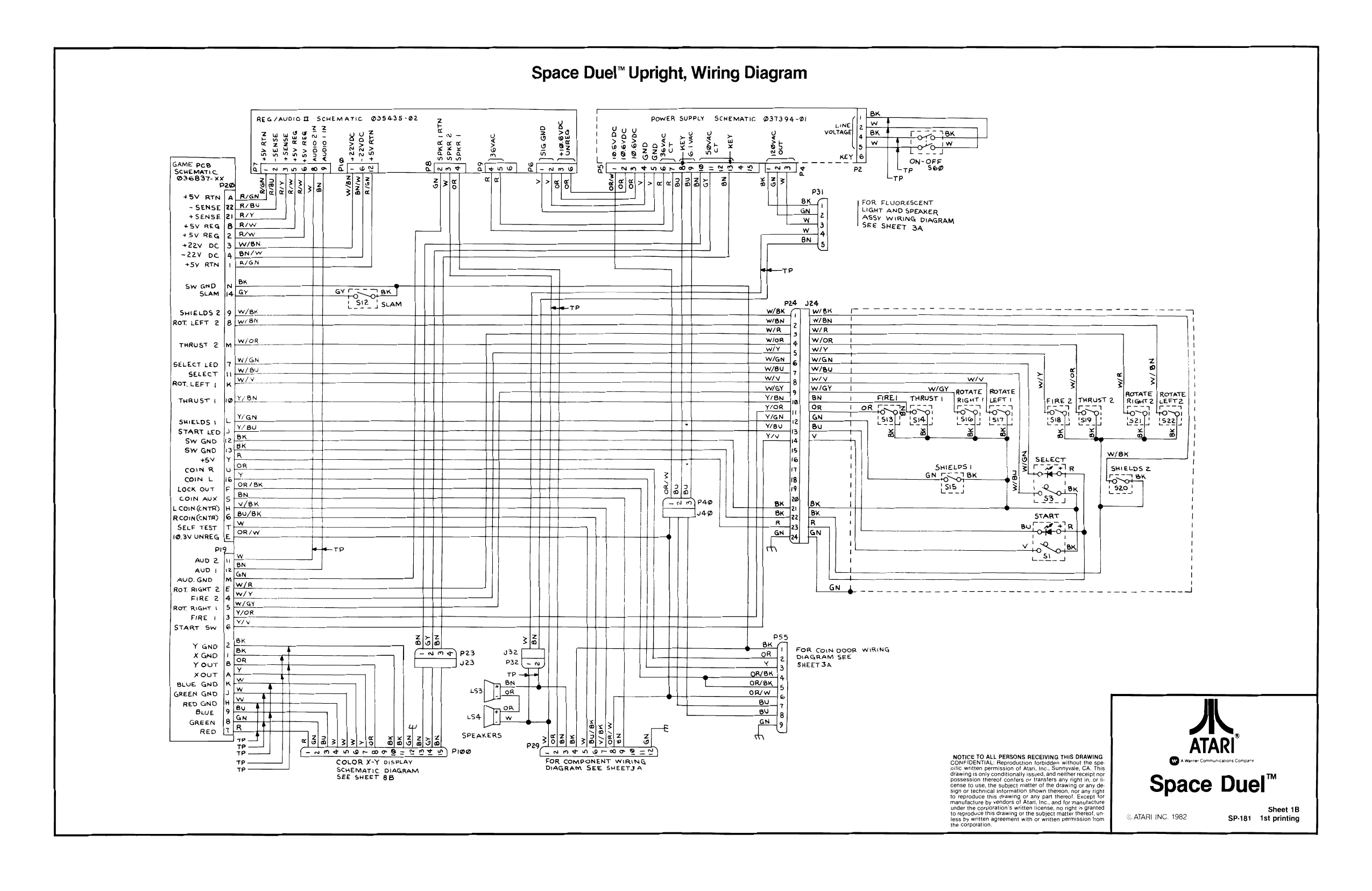
This page is a drawing, shown as the original scan.
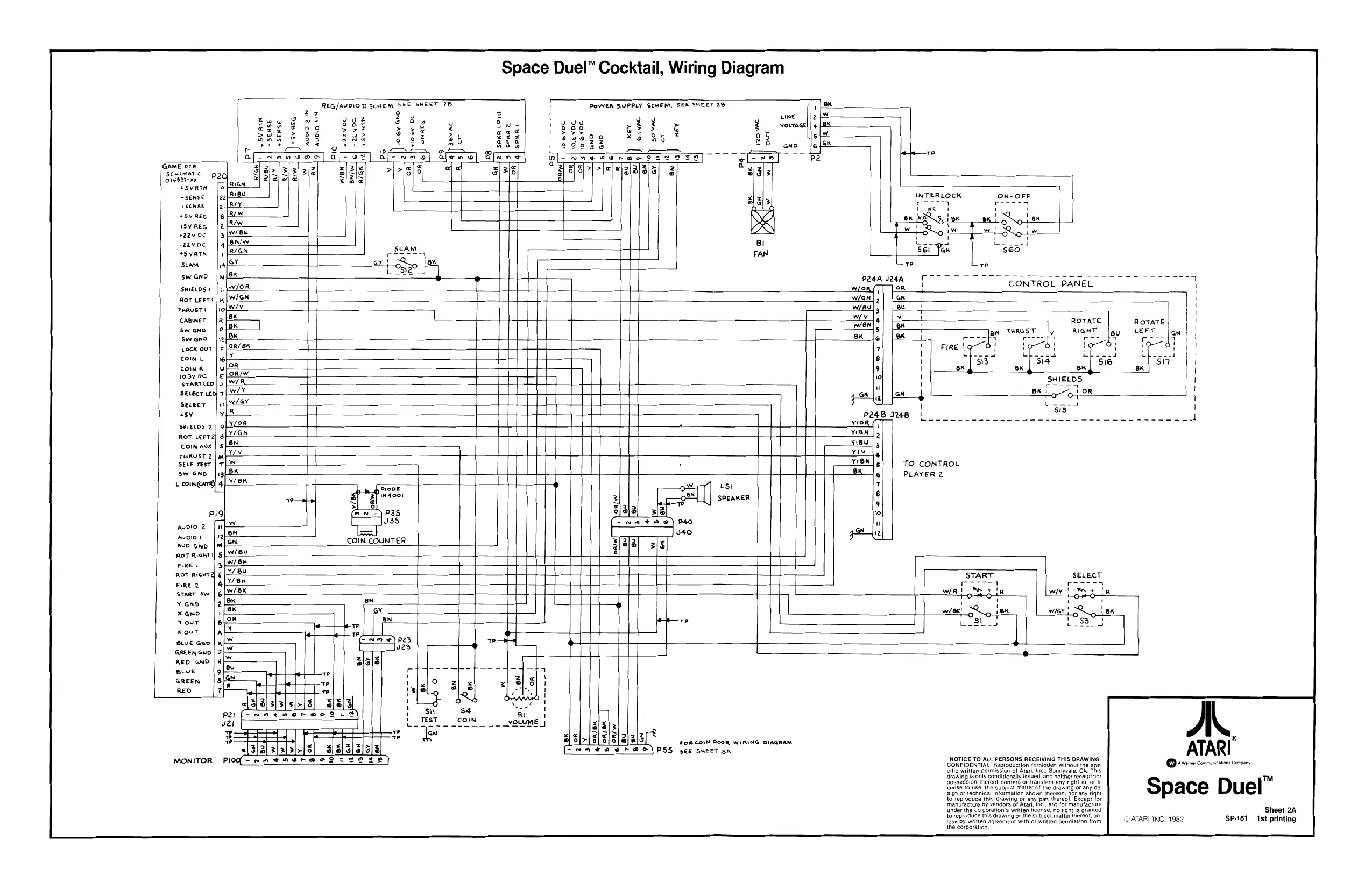
This page is a drawing, shown as the original scan.
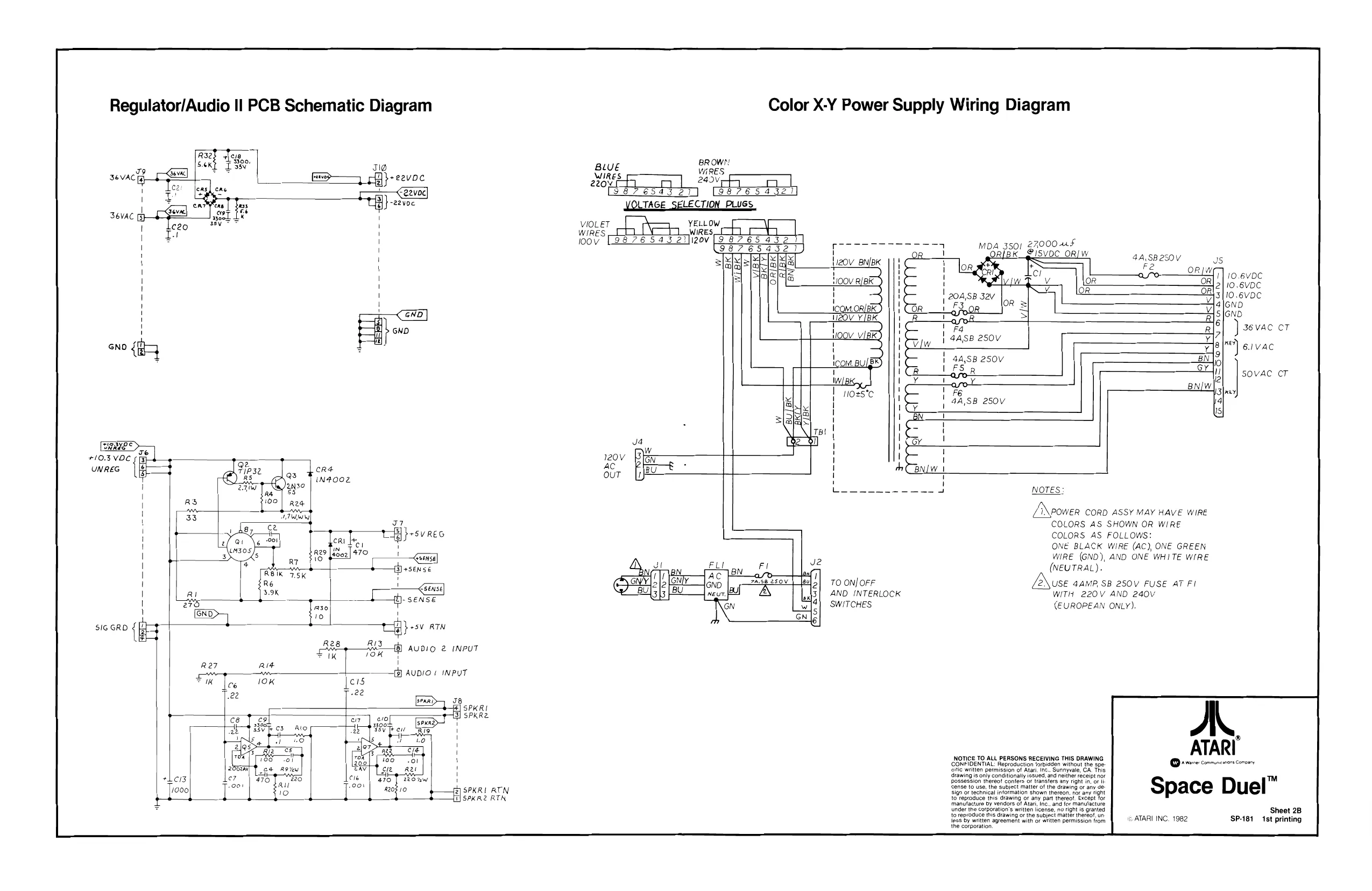
This page is a drawing, shown as the original scan.
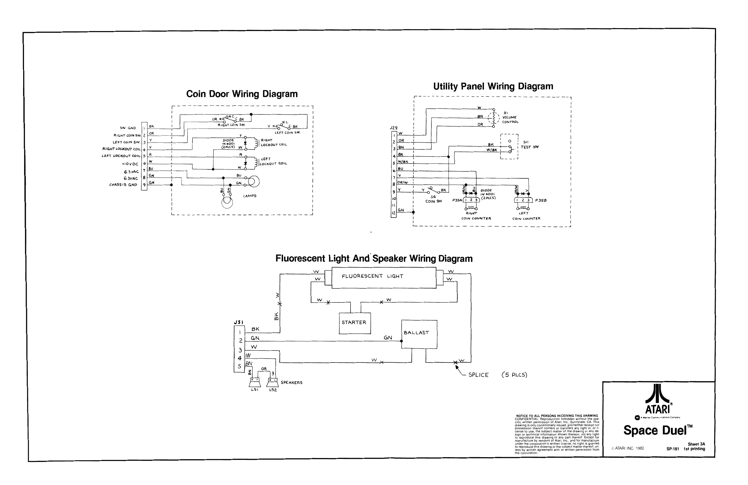
Coin Door Wiring Diagram Utility Panel Wiring Diagram
we on woRS Cc BK RIGHT COIN SW. Sw. GND
RIGHT COIN Sw, y DIODE RIGHT
RIGHT LocKouT cow
LEFT LOCKOUT Con ’
LEFT con Sw.| 3
cEFT tlovoe | Lockour cor.
6.3vAc |T 6.3vac |8 CHASS!S GND [3 aL a) oiove im 4001 ip din aney (apices) RIGHT COIN COUNTER
w w. FLUORESCENT LIGHT 7}
—o
STARTER
BALLAST GN Tt... XN SPLICE (5 PLCS) SPEAKERS A
ATARI
Qe connenens concn NOTICE TO ALL PERSONS RECEIVING THIS DRAWING CONFIDENTIAL Reproduction forbidden without the spe Giic written permission of Atari, Inc, Sunnyvale, CA. This SGrawing is omy conaitionally issued, ana neither receipt nor poscession thereat confers or transfers any right in, or S ™ Gense tovuse, the subject matter of the drawing ov any de ce {reproduce this Grawing or any pat thereot Except for mandlactre by vender ot Naty ord or manulacte Under the corporation's writen license, no ight fe gran Sheet 3A jorreproasce ts drawing or the subject matter there Un : s less by writen agreement with or waen permission from ATARI INC. 1982 SP-181 1st printing the corseration
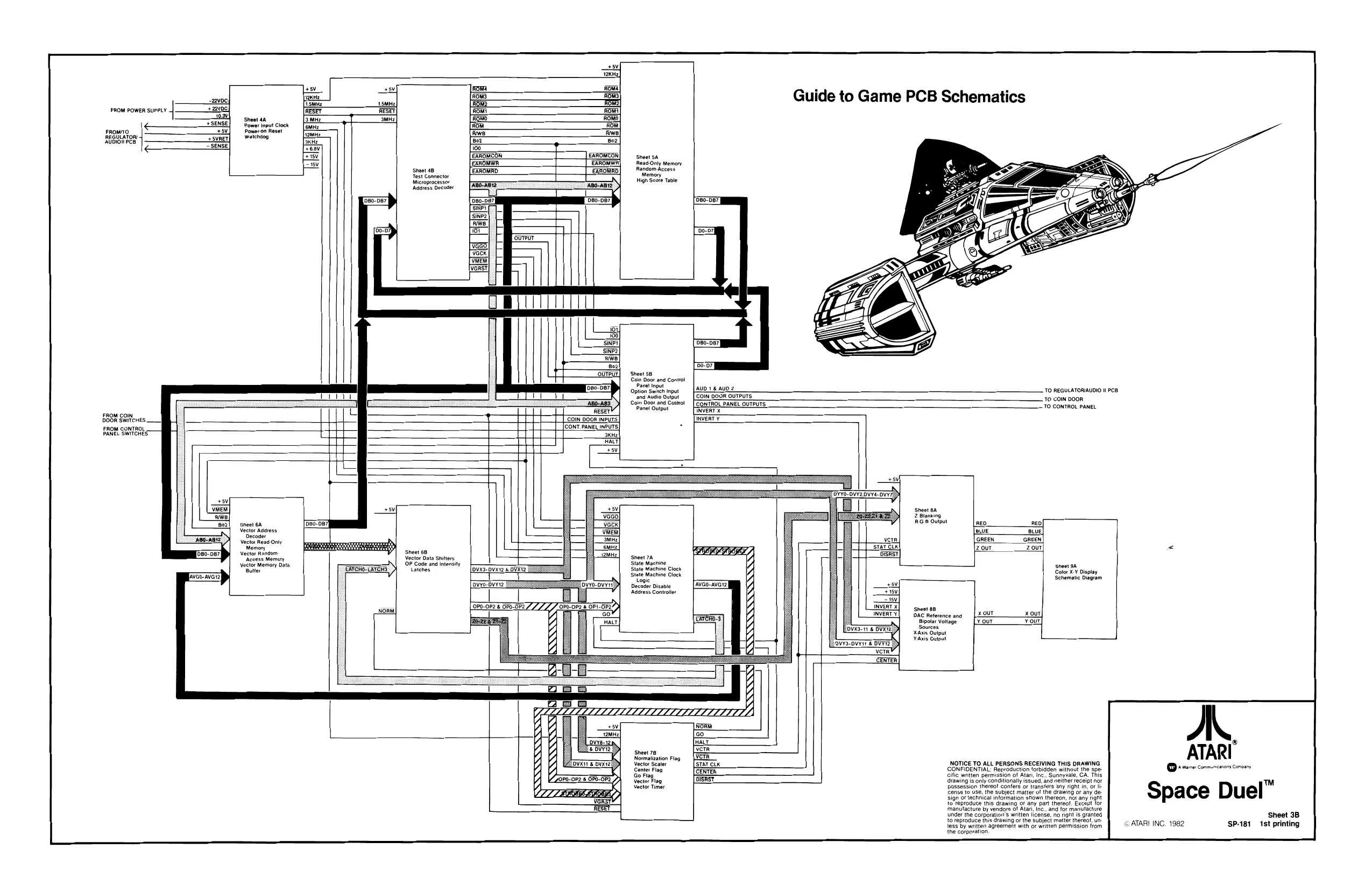
This page is a drawing, shown as the original scan.
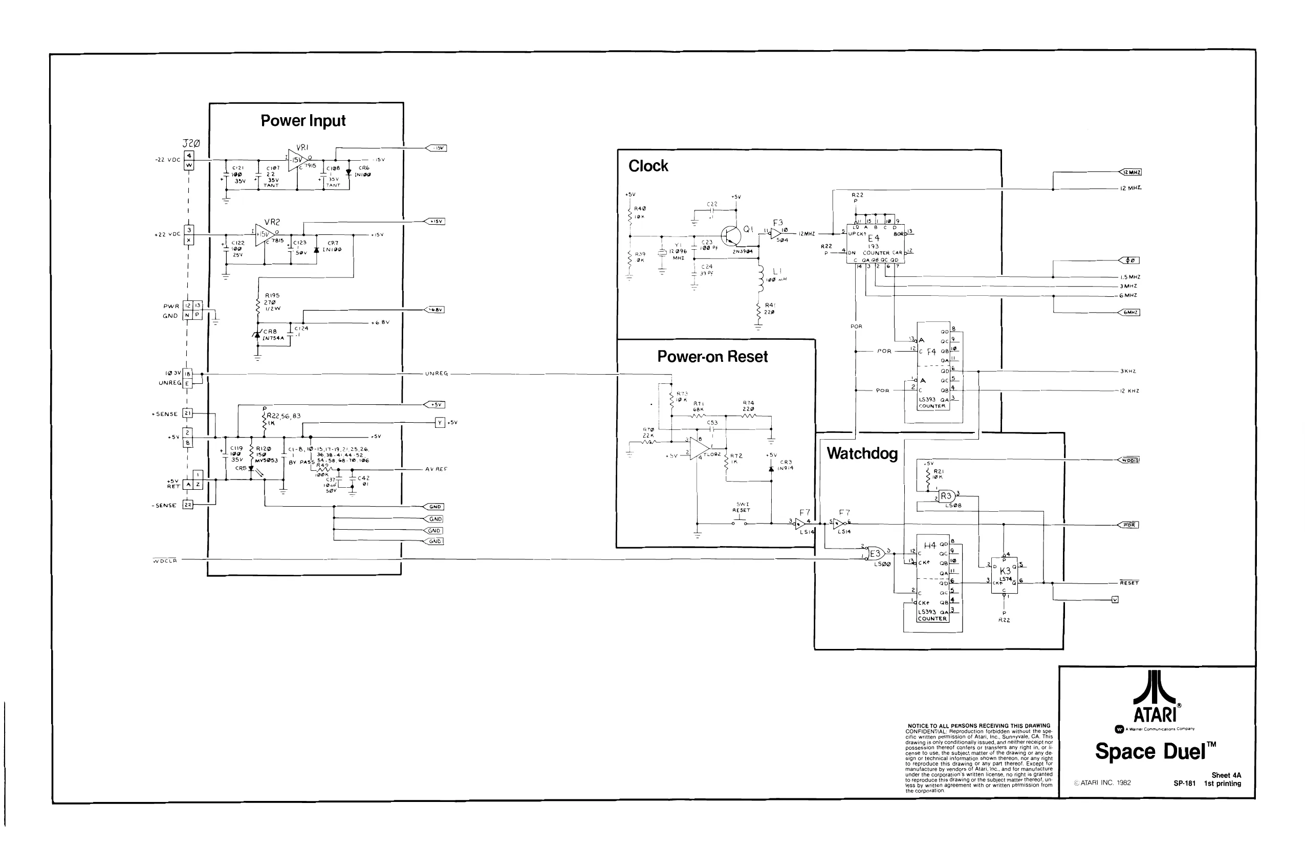
This page is a drawing, shown as the original scan.
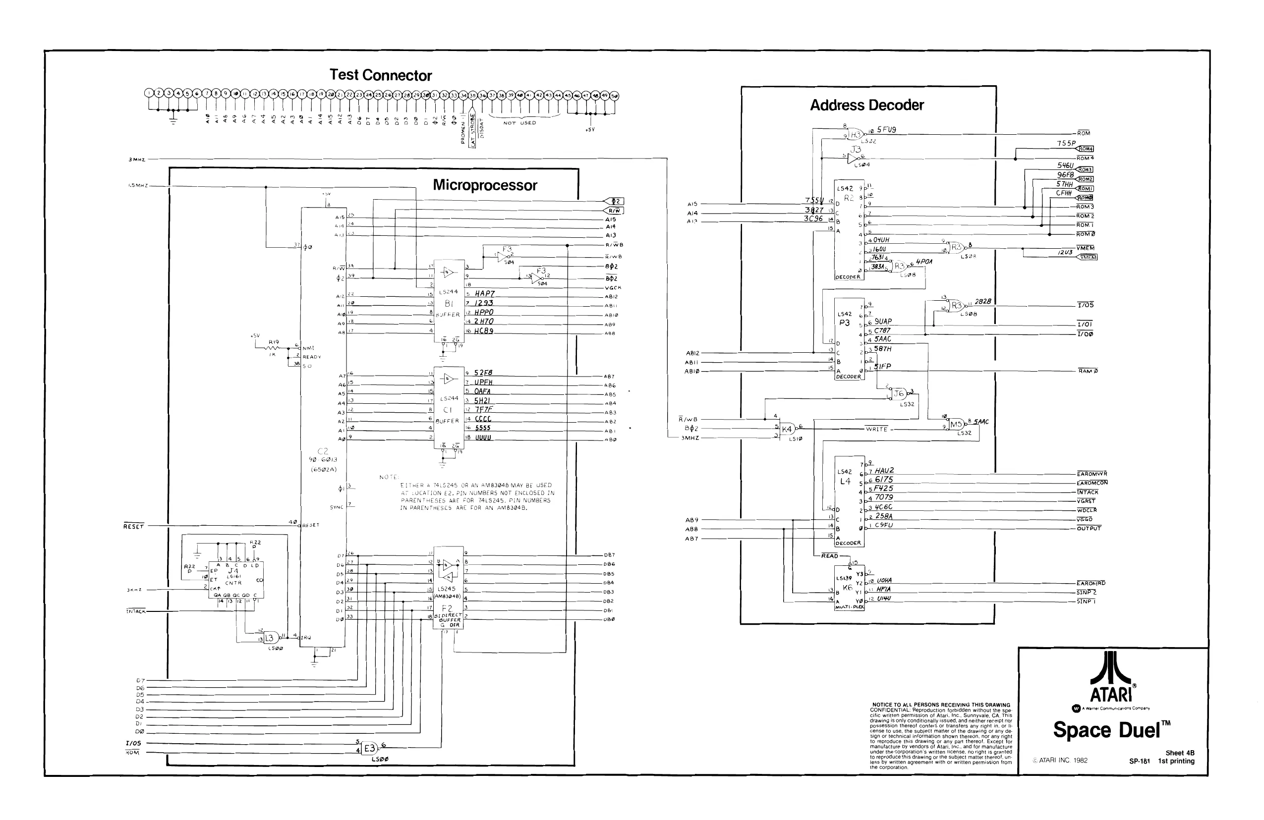
This page is a drawing, shown as the original scan.
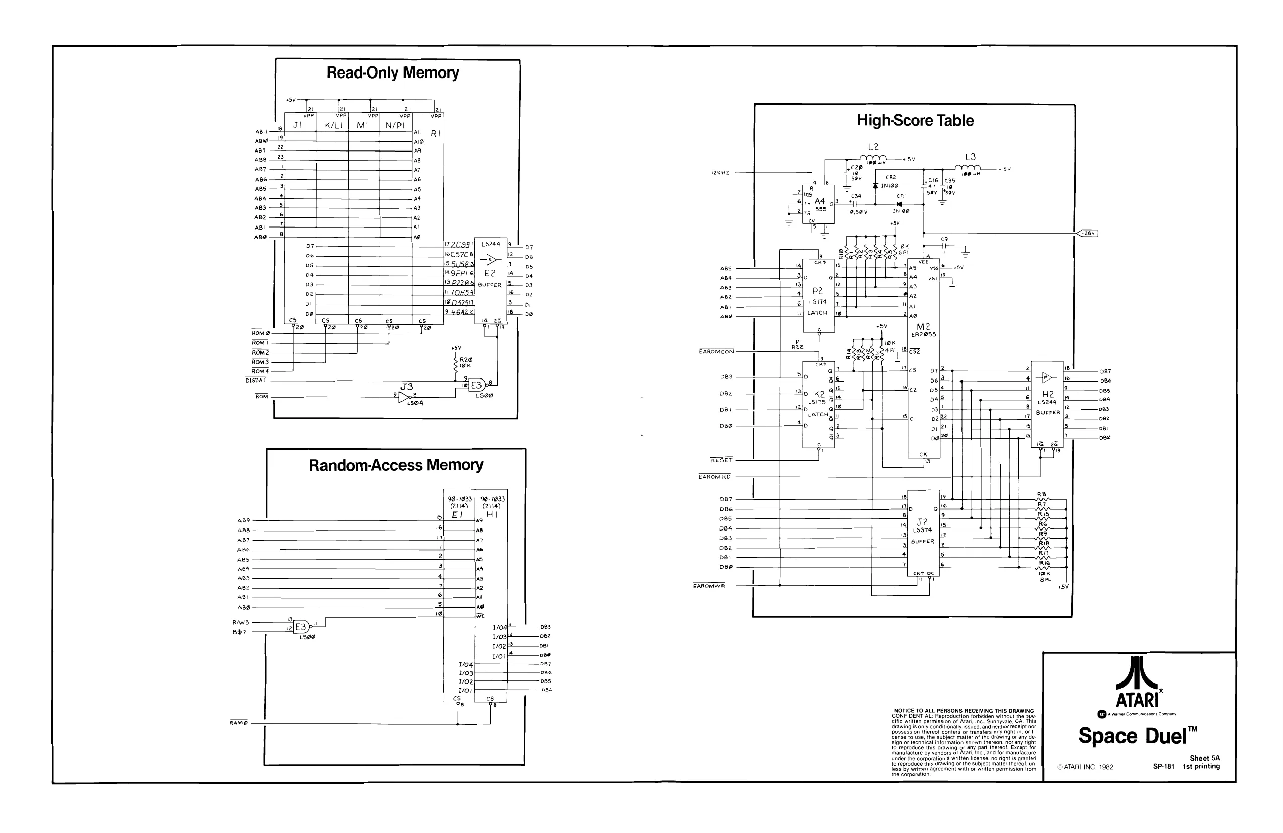
This page is a drawing, shown as the original scan.
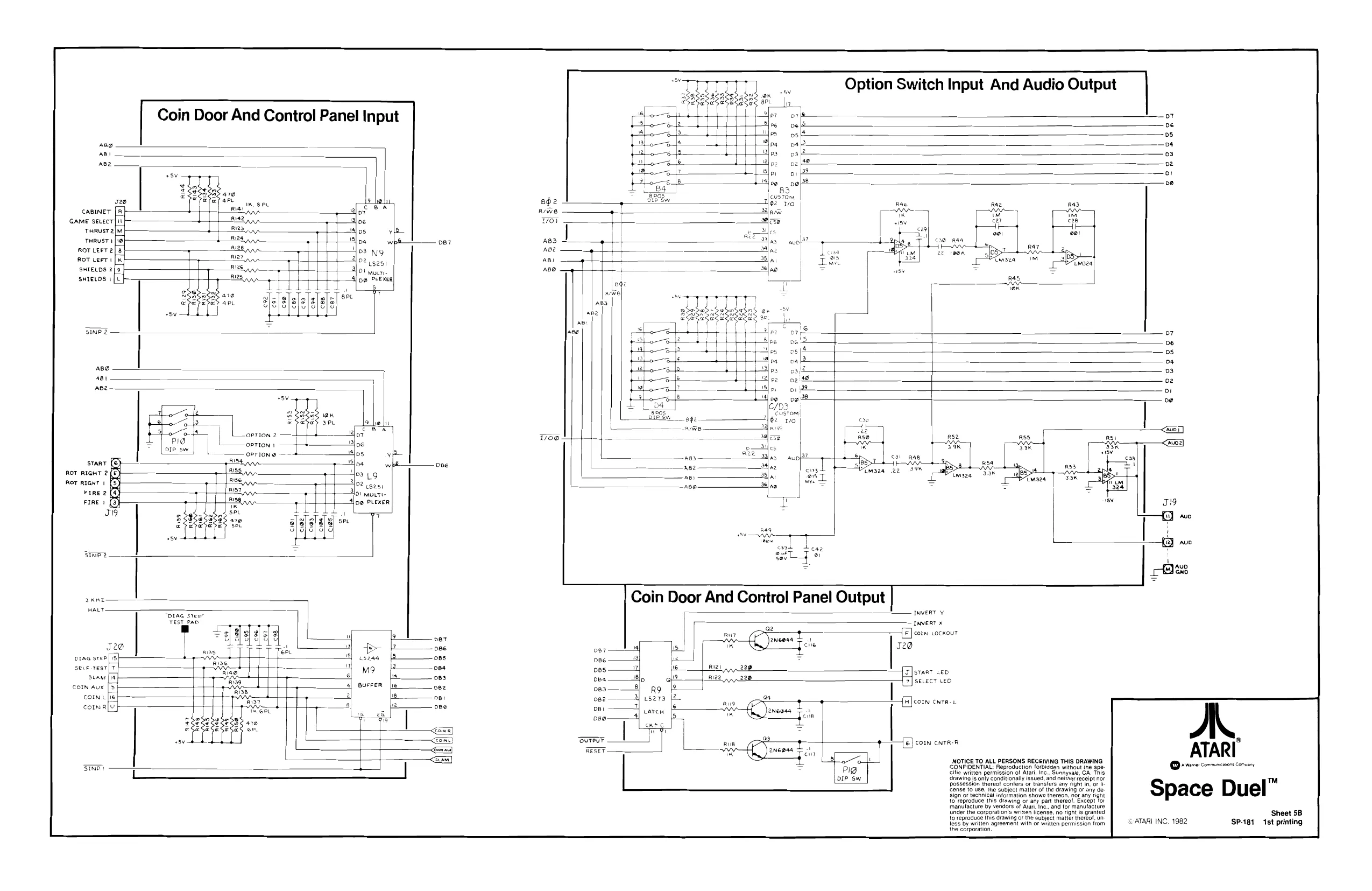
This page is a drawing, shown as the original scan.
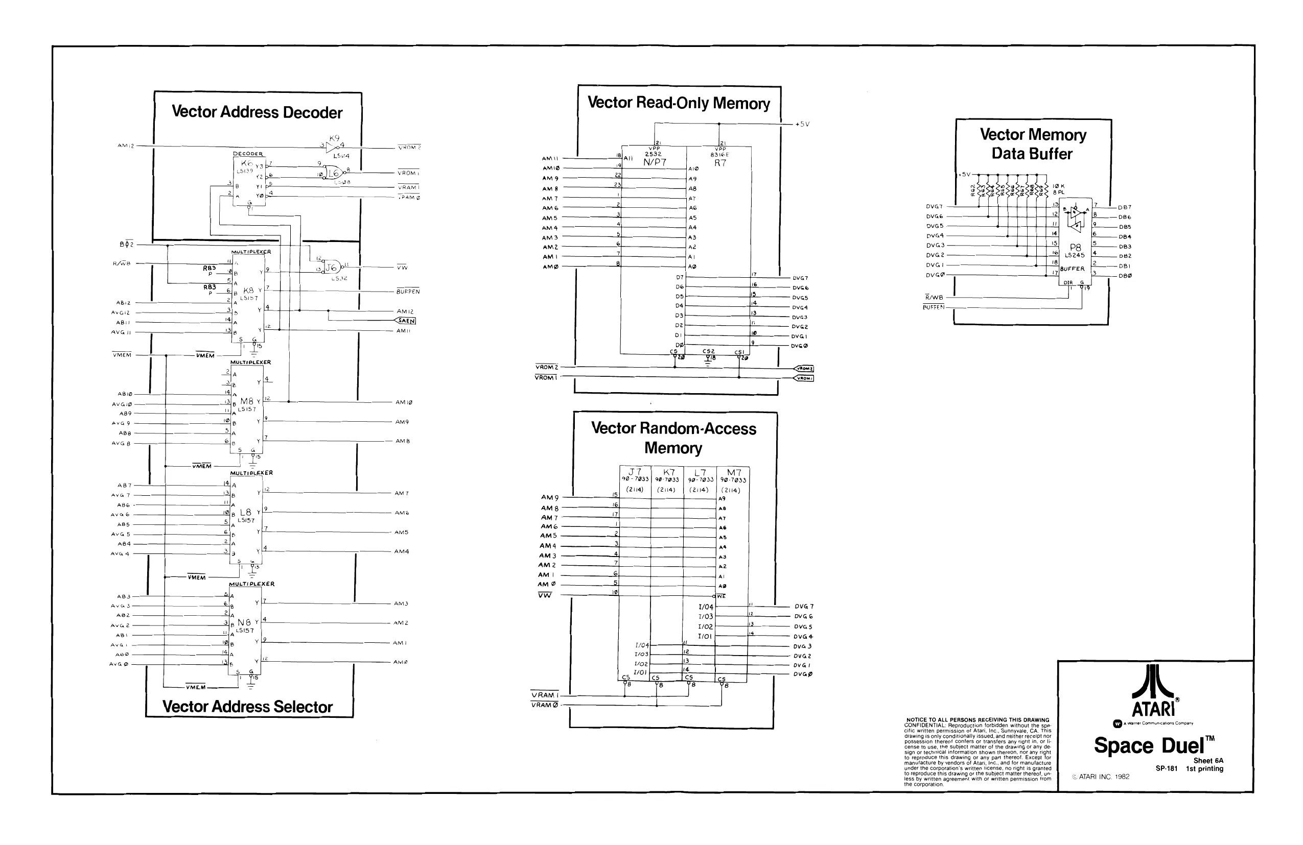
This page is a drawing, shown as the original scan.
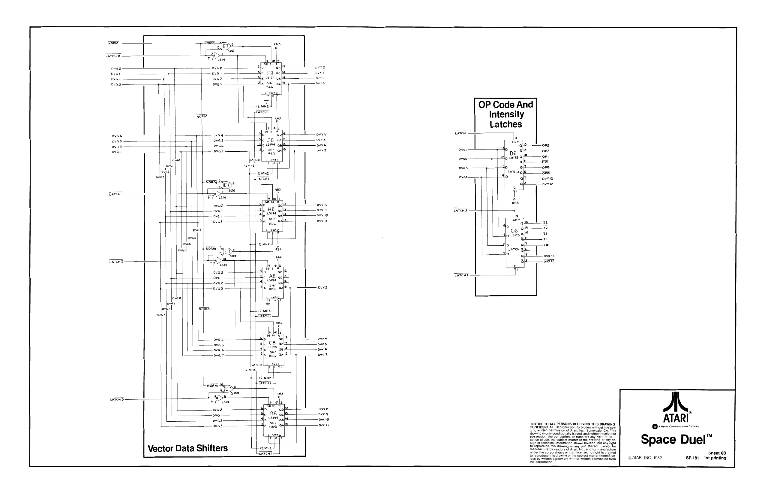
This page is a drawing, shown as the original scan.
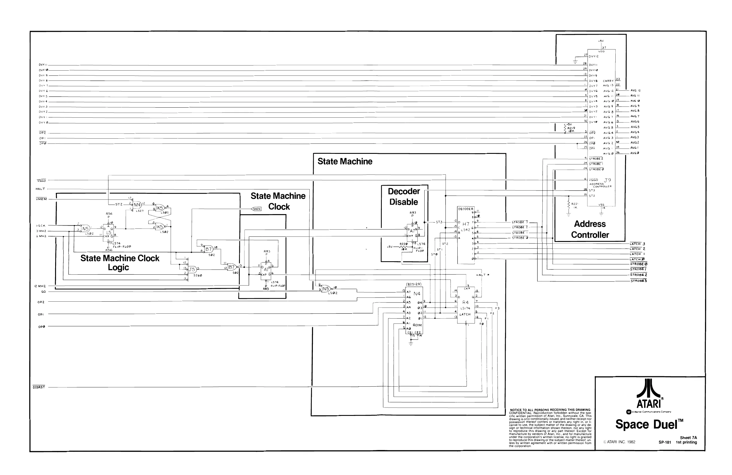
This page is a drawing, shown as the original scan.
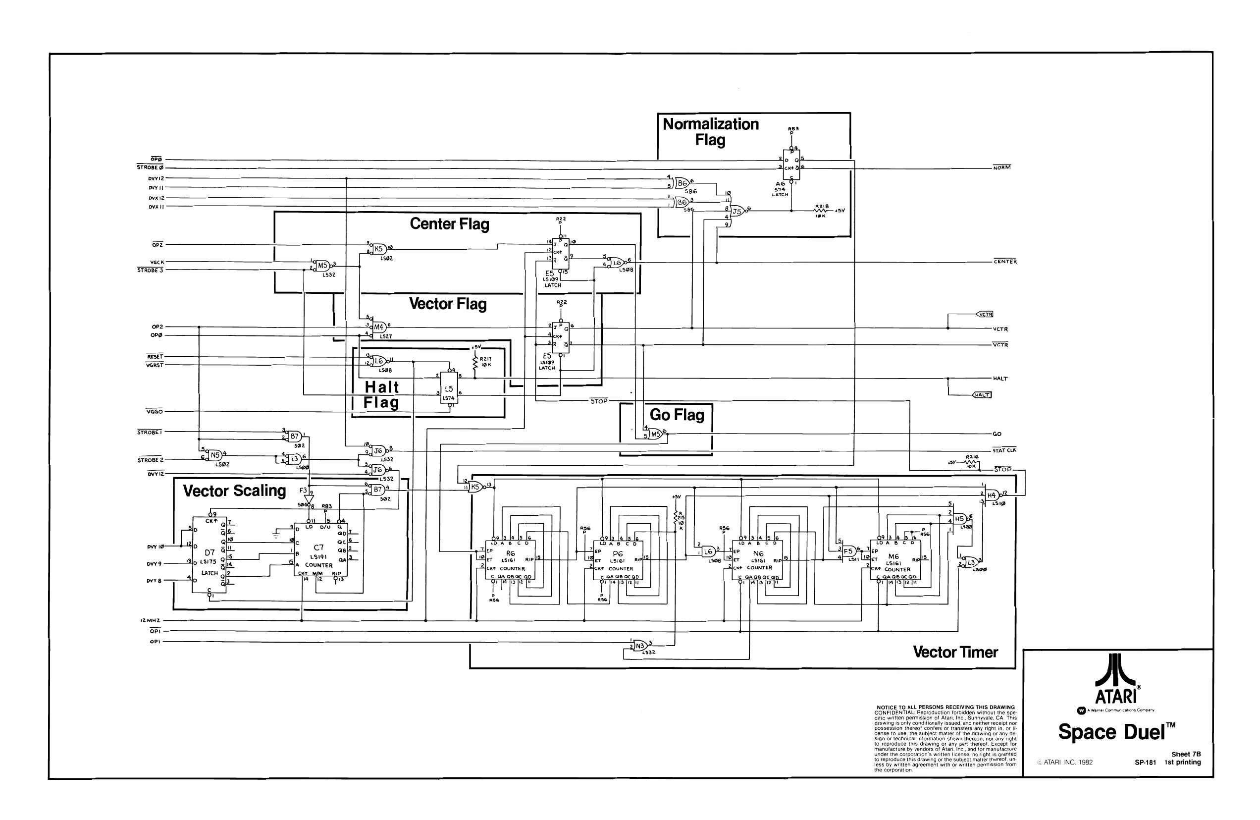
This page is a drawing, shown as the original scan.
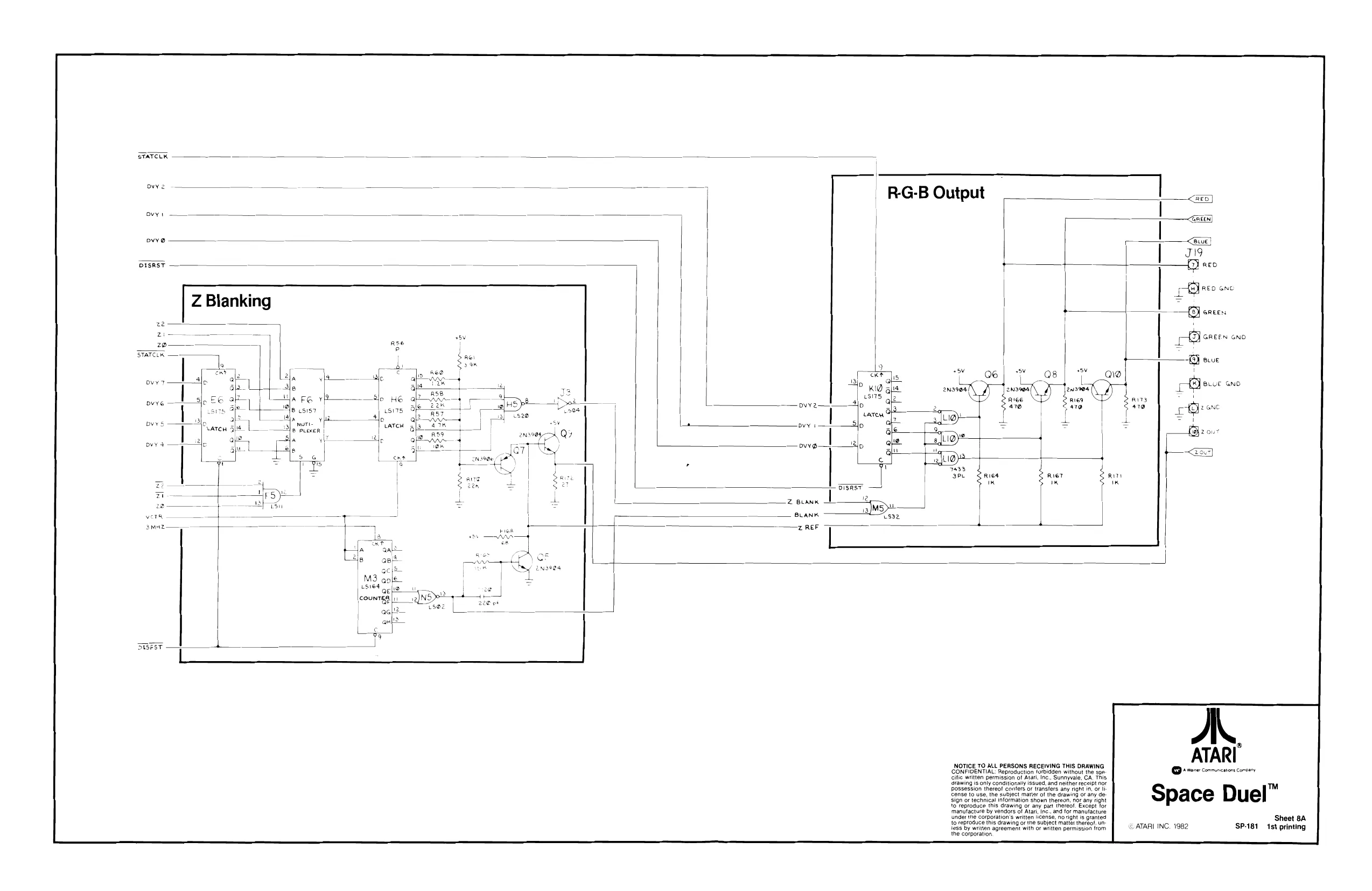
This page is a drawing, shown as the original scan.
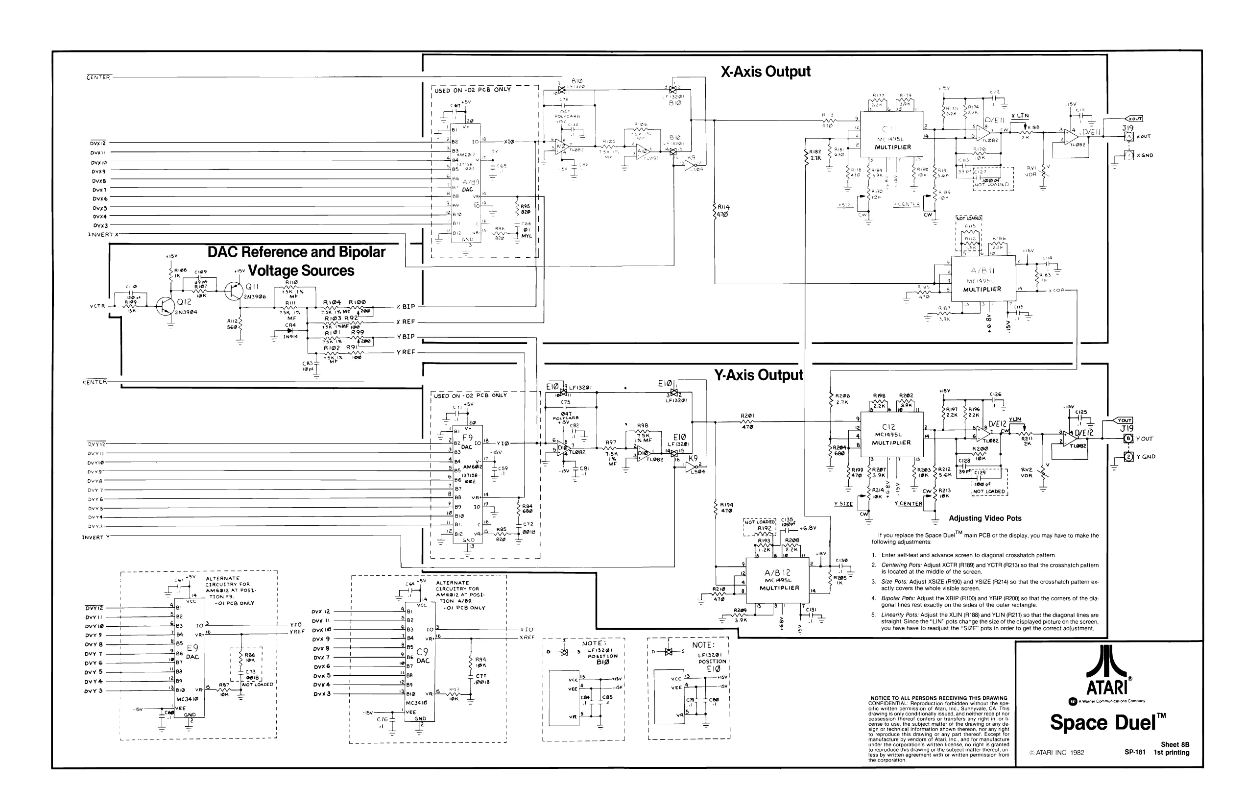
This page is a drawing, shown as the original scan.
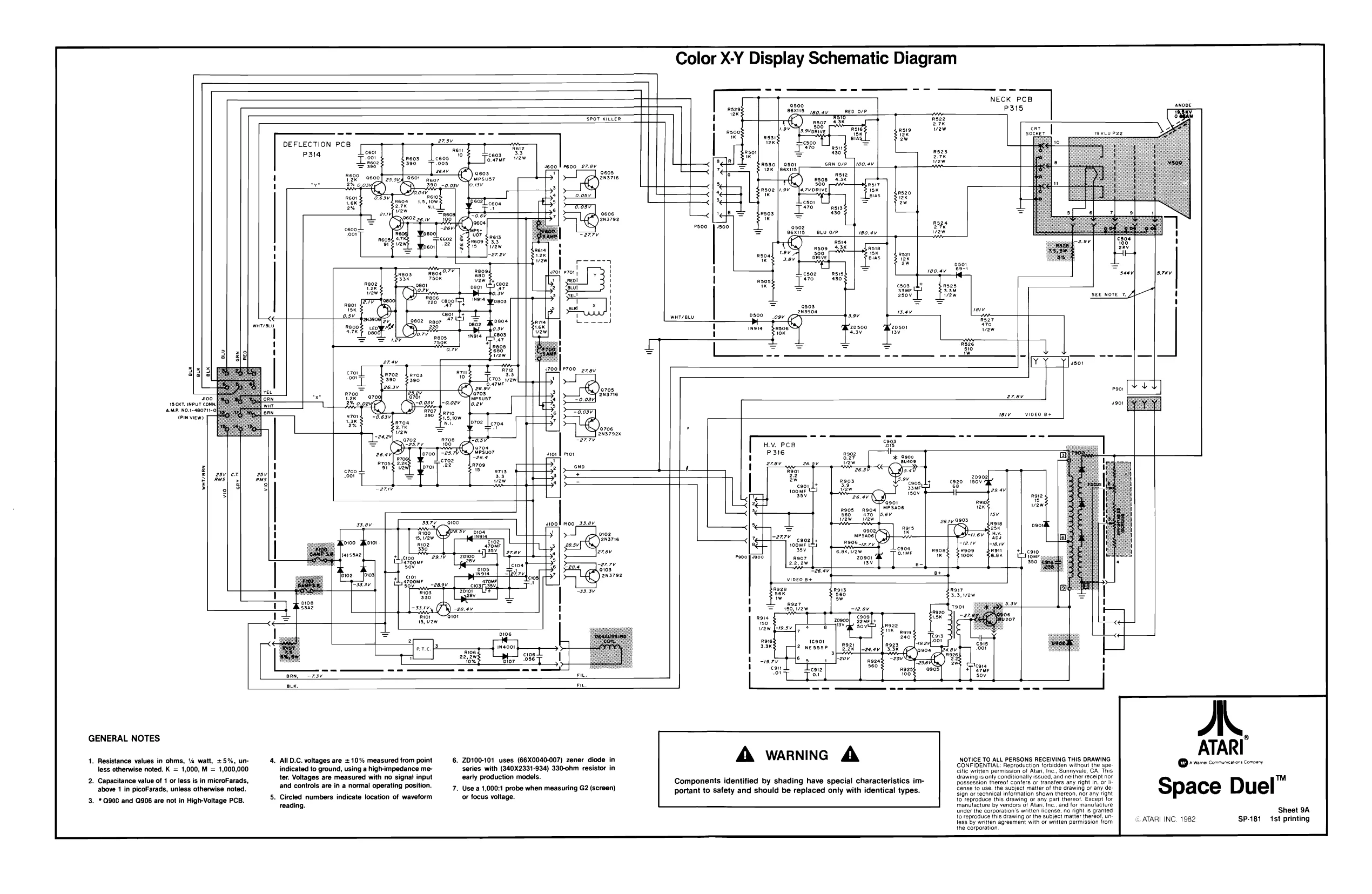
Color X-Y Display Schematic Diagram
SPOT KILLER
DEFLECTION PCB P34 NECK PCB P315,
sewer, toviv pee
°700_enav
sscer. PUT CONN AMP NO.I-AB071"-Of comview)
o706 pee
0502 aeens Lu oP
asia
see nore 24
oo 35.84
ansri6
lexev
103.
ioe Blor 23H
GENERAL NOTES
|. Resistance values in ohms, % watt, +5%, unless otherwise noted. K = 1,000, M = 1,000,000 . Capacitance value of 1 or less is in microFarads, above 1 in picoFarads, unless otherwise noted.
- 900 and Q906 are not in High-Voltage PCB. 4. AILD.C. voltages are + 10% measured from point indicated to ground, using a high-impedance meter. Voltages are measured with no signal input and controls are in a normal operating position. . Circled numbers indicate location of waveform reading.
- ZD100-101 uses (66X0040-007) zener diode in series with (340X2331-934) 330-ohm resistor in early production models.
7. Use a 1,000:1 probe when measuring G2 (screen)
oF focus voltage.
A warninc A
Components identified by shading have special characteristics important to safety and should be replaced only with identical types. NOTICE TO ALL PERSONS RECEIVING THIS DRAWING CONFIDENTIAL: Reproduction forbidden without the spe Gifc written permission of Atari, Inc, Sunnyvale. CA. This Srawing is only conditionally issued, and netiner receipt nor possession thereo! confers or transfers any right In, OF I Eense to.use, the subject matter of the drawing or any de Sign of technical information shown thereon, nor any right to reproduce this drawing or any part thereal. Except for manufacture by vendors of Atar nc, and for manufacture Under the corporation's written license, no night Is granted to reproduce this drawing oF te subject matter thereo!. ur Tess by writen agreement with or written permission from the corporation AL ATARI" tier cormncarons coneary
Space Duel”
Sheet 9A © ATARI INC. 1982 SP-181 1st printing
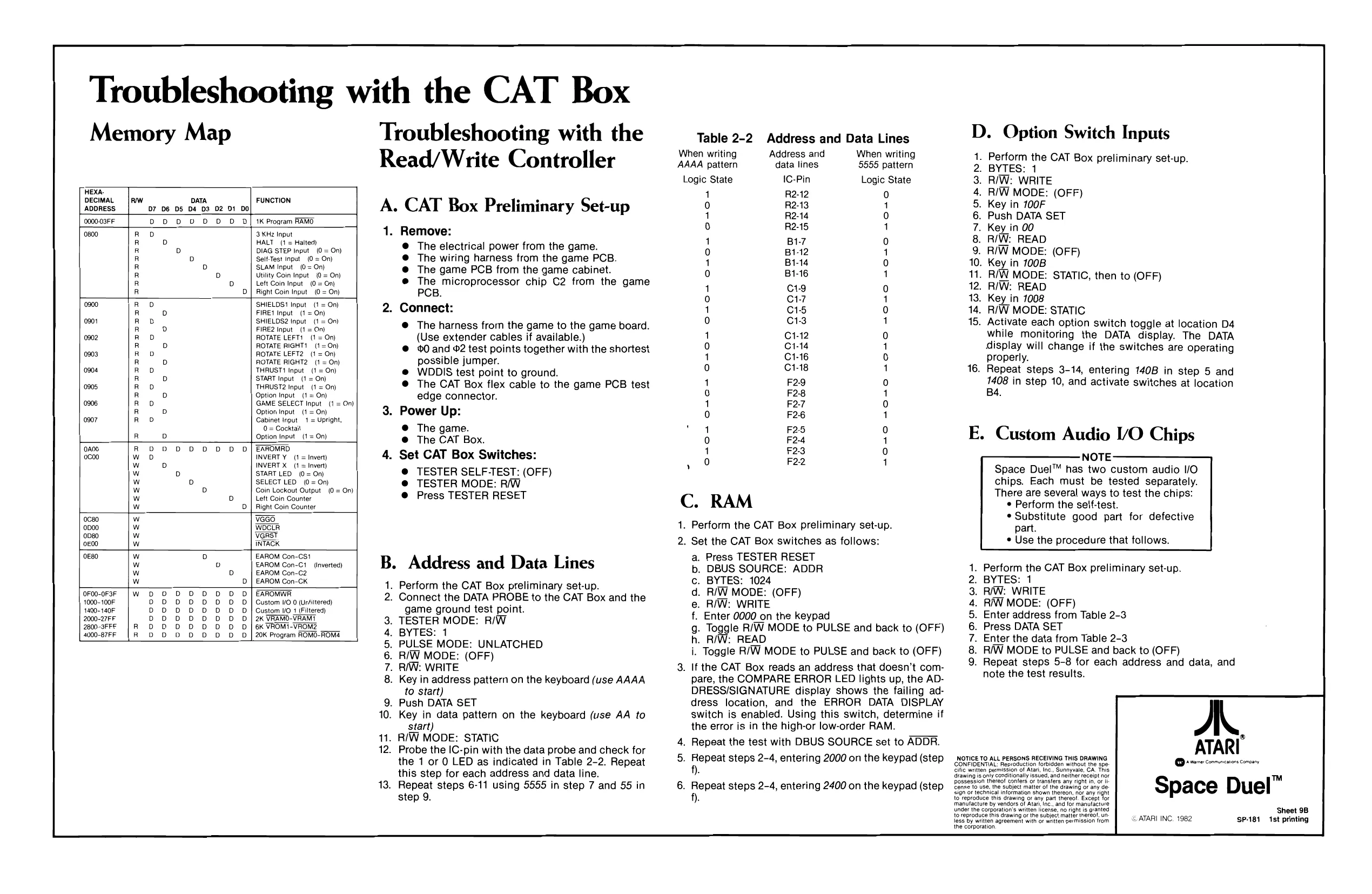
Troubleshooting with the CAT Box
Troubleshooting with the
Memory Map
| HEXA- DECIMAL ADDRESS DATA D6 D5 D4 D3 02 01 DO FUNCTION
(0000.03FF ooovoODODD 1K Program RAMO 0800 D 3.KHz Input HALT (1 = Halted) DIAG STEP Input (0 = On) Self-Test Input (0 = On) SLAM Input (0 = On) Utility Coin Input (@= On) Left Coin Input (0 = On) Right Coin Input _(0 = On) DD DDD DDD TV VDDDD| DVD VPADD
SHIELDS1 Input (1 = On)
FIRE! Input (1 = On) SHIELDS2 Input (1 = On) FIRE2 Input _(1 = On) ROTATE LEFT! ROTATE RIGHT! (1=On) ROTATE LEFT2 (1 = On)
ROTATE RIGHT2 (1 = On)
THRUST2 Input
Option input (1 = On)
GAME SELECT Input (1 = On) Option Input (1 = On) Cabinet Input 1 = Upright, 0 = Cocktait Option Input_(1= On) EAROMRD INVERT Y_ (1 = Invert) INVERT X_ (1 = Invert) START LED (0 = On) SELECT LED (0 = On) Coin Lockout Output (0 = On) Left Coin Counter Right Coin Counter Vaso WOCLR vaast INTACK EAROM Con-CSt EAROM Con-C1 (Inverted) EAROM Con-C2 EAROM Con-Ck (OF 00-OF 3F| 1000-100F 1200-140F 2000-27FF 2800-3F FE 4000-87FF S| Sesslsssslssssesex|n EAROMWR Custom 1/0 0 (Unfiltered) Custom 1/0 1 (Filtered) 2k VRAMO-VRAMT 20K Program ROMO-ROM4 Read/Write Controller
A. CAT Box Preliminary Set-up
1.
2.
3.
4.
B.
1. 2. Remove: @ The electrical power from the game. @ The wiring harness trom the game PCB. @ The game PCB from the game cabinet. @ The microprocessor chip C2 from the game PCB. Connect:
@ The harness from the game to the game board. (Use extender cables if available.) @ 0 and #2 test points together with the shortest possible jumper. @ WDDIS test point to ground. @ The CAT Box flex cable to the game PCB test edge connector. Power Up: @ The game. @ The CAT Box. Set CAT Box Switches: @ TESTER SELF-TEST: (OFF) @ TESTER MODE: RW @ Press TESTER RESET
Address and Data Lines
Perform the CAT Box preliminary set-up. Connect the DATA PROBE to the CAT Box and the game ground test point. . TESTER MODE: R/W
7. 8.
9. 10.
11. 12.
13.
- BYTES: 1 5.
- R/W MODE: (OFF) PULSE MODE: UNLATCHED
RW: WRITE Key in address pattern on the keyboard (use AAAA to start) Push DATA SET Key in data pattern on the keyboard (use AA to start) R/W MODE: STATIC Probe the IC-pin with the data probe and check for the 1 or 0 LED as indicated in Table 2-2. Repeat this step for each address and data line. Repeat steps 6-11 using 5555 in step 7 and 55 in step 9. Table 2-2 Address and Data Lines
| When writing | Address and | When writing |
| AAAA pattern | data lines | 5555 pattern |
| Logic State | IC-Pin | Logic State |
R2-12 R2-13 R2-14 R2-15 B17 B1-12 B1-14 B1-16 C1-9 C1-7 C15 C1-3 C1-12 C1-14 C1-16 C1-18 F29 F2-8 F2-7 F2-6 F25 F2-4 F2-3 F22 O404 C464 C404 C404 C404 CHAo4 40420 24040 4040 4040 Aono Aono
C. RAM . Perform the CAT Box preliminary set-up. . Set the CAT Box switches as follows: a. Press TESTER RESET b. DBUS SOURCE: ADDR c. BYTES: 1024 d. R/W MODE: (OFF) e. R/IW: WRITE f. Enter 0000 on the keypad g. Toggle R/W MODE to PULSE and back to (OFF) h. R/W: READ i. Toggle R/W MODE to PULSE and back to (OFF) . If the CAT Box reads an address that doesn’t compare, the COMPARE ERROR LED lights up, the AD- DRESS/SIGNATURE display shows the failing address location, and the ERROR DATA DISPLAY switch is enabled. Using this switch, determine if the error is in the high-or low-order RAM. . Repeat the test with DBUS SOURCE set to ADDR. . Repeat steps 2-4, entering 2000 on the keypad (step f). . Repeat steps 2-4, entering 2400 on the keypad (step f. D. Option Switch Inputs
Perform the CAT Box preliminary set-up. BYTES: 1 R/W: WRITE R/W MODE: (OFF) Key in 100F Push DATA SET Key in 00 RW: READ . R/W MODE: (OFF) . Key in 100B . R/W MODE: STATIC, then to (OFF) . RIW: READ Key in 7008 . _R/W MODE: STATIC . Activate each option switch toggle at location D4 while monitoring the DATA display. The DATA display will change if the switches are operating properly. . Repeat steps 3-14, entering 140B in step 5 and a in step 10, and activate switches at location PONOMAROMS
Custom Audio O Chips
. Perform the CAT Box preliminary set-up. BYTES: 1 RIW: WRITE RIW MODE: (OFF) Enter address from Table 2-3 . Press DATA SET . Enter the data from Table 2-3 . RW MODE to PULSE and back to (OFF) . Repeat steps 5-8 for each address and data, and
0 ATARI
Space Duel”
Sheet 9B ‘SP-181 1st printing OMNATARONS
NOTICE TO ALL PERSONS RECEIVING THIS DRAWING CONFIDENTIAL: Reproduction forbidden without the spe. fille written peeission of Atari Inc, Sunnyvale, CA. This Sawing ort coniionally Issued, dnanetner eCopt nor osgession tereo! conters or transfers any right in, oF PGase To use, the Subject matter ol ne drawing or any de sign or technical informatian shown thereon, nor any "ight to reproduce this. drawing or any part thereo!, Except for manulacture by vendors ot Atari, Inc, and Tor manufacture Under the corporation's waitten license, no night Is granted to reproduce this drawing or the subject. matter thereo!, un less by written agreement with or written permission trom the corporation ATARI INC. 1982
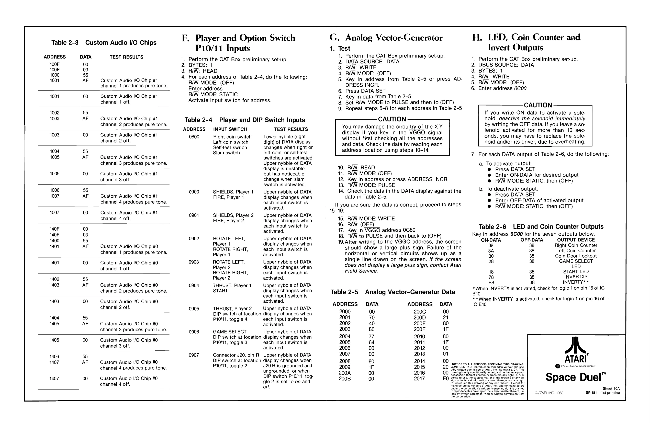
F. Player and Option Switch G. Analog Vector-Generator H. LED, Coin Counter and
| P10/11 Inputs | 1. Test | Invert Outputs | ||||||
| ADDRESS | DATA | TEST RESULTS | . Perform the CAT Box preliminary set-up. | OO OSCE: Dame | nay Setup | . Perform the CAT Box preliminary set-up. | ||
| {00F | Fs | SD | ; RW: WRITE | .. DBUS'SOURCE: DATA | ||||
| 1000 | 55 | - For | each address | of | Table 2-4, do | the following: | | BW MODE: (OFF) | - RW: WRITE |
| 4001 | AF | Custom Audio VO Chip #1 | - | For each address of Table 2-4, do | the following: | ; Key in address from Table 2-5 or press AD- | 4 | RW: |
RIW MODE: (OFF) . RW MODE: (OFF) channel 1 produces pure tone. DRESS INCR.
| Enter address | - Press DATA SET | . Enter address 0C00 | ||
| 1001 | 00 | Custom Audio I/O Chip #1 | RIW MODE: STATIC | . Key in data from Table 2-5 |
| channel 1 off. | Activate input switch for address. | ; Set RW MODE to PULSE and then to (OFF) | CAUTION |
. Repeat steps 5-8 for each address in Table 2-5 j 1002 If you write ON data to activate a sole-
| 1003 | Custom Audio I/O Chip #1 | Table 2-4 | Player and DIP Switch Inputs | CAUTION | noid, deactive the solenoid immediately | |
| channel 2 produces pure tone. | iit | iti | . | - | ||
| P | : | ADDRESS | INPUT SWITCH | TEST RESULTS | You may damage the circuitry of the X-Y | in ata ie oa data. I ote ait md |
display if you key in the VGGO signal lenoid activated for more than 10 sec
| 1003 | Custom Audio VO Chip #1 | 0800 | Right coin switch | Lower nybble (right | without first checking all the addresses | onds, you may have to replace the sole- |
| channel 2 off. | Left coin switch | digit) of DATA display | and data. Check the ae by reading each | noid and/or its driver, due to overheating. | ||
| 1004 | eee ound | piace pie | address location using steps 10-14: | |||
| 1005 | Custom Audio I/O Chip #1 | switches are activated. | ||||
| channel 3 produces pure tone. | Upper nybble of DATA | — | a. To activate output: | |||
| display is unstable, | 10. RIW: READ | @ Press DATA SET | ||||
| 1005 | Custom Audio I/O Chip #1 | but has noticeable | 11. R/W MODE: (OFF) | @ Enter ON-DATA for desired output | ||
| channel 3 off. | change when slam | 12. Key in address or press ADDRESS INCR. | @ RIW MODE: STATIC, then (OFF) | |||
| switch is activated. | 13. RIW MODE: PULSE | : | ||||
| 1006 | , | , | SHIELDS, Player 1 | Upper nybble of DATA | 14. Check the data in the DATA display against the | |
| 1007 | Custom Audio VO Chip #1 | FIRE, Player 1 | display changes when | data in Table 2-5. |
channel 4 produces pure tone. each input switch is Table 2-3 Custom Audio I/O Chips
- For each DATA output of Table 2-6, do the following:
b. To deactivate output: @ Press DATA SET . @ Enter OFF-DATA of activated output
| activated. | If you are sure the data is correct, proceed to steps | @ RIW MODE: STATIC, then (OFF) | |||||||
| 1007 | Custom Audio VO Chip #1 | 15-19: | |||||||
| SHIELDS, Player 2 | Upper nybble of DATA | . | |||||||
| channel 4 off. | FIRE, Player 2 | display changes when | 15. R/W MODE: WRITE | ||||||
| MOF | each input switch is | c Rey Is WORD address 0C80 | Table 2-6 | LED and Coin Counter Outputs | |||||
| 140F | ROTATE LEFT. | Upper nybble of DATA | 18. R/W to PULSE and then back to (OFF) | Key in address 0C00 for the seven outputs below. | |||||
| 1400 | 7 | 19. After writing to the VGGO address, the screen | ON-DATA | OFF-DATA | OUTPUT DEVICE | ||||
| . | Player 1 | display changes when | . | A | i | ||||
| 1401 | Custom Audio I/O Chip #0 | eee | 33 | 38 | Right Coin Counter | ||||
| ROTATE RIGHT, | each input switch is | should show a large plus sign. Failure of the | 3A | 38 | Left Coin Counter | ||||
| channel 1 produces pure tone. | ; | i | i | feet | |||||
| 1401 | Custom Audio I/O Chip #0 | ROTATE LEFT, | Upper nybble of DATA | . | poh | . | 28 | 38 | GAME SELECT |
| channel 1 off. | e | Player 2 | display changes when | does not display a large plus sign, contact Atari | LED |
ROTATE RIGHT, each input switch is Field Service. 18 38 START LED
| 1402 | Player 2 | activated. | 78 | 38 | ene | ||
| " | , | B8 | 38 | aa | |||
| 1403 | Custom Audio I/O Chip #0 | THRUST, Player 1 | Upper nybble of DATA | 7 | - | f | 1 |
, i *When INVERTX is activated, check for logic 1 on pin 16 of IC
| channel 2 produces pure tone. | START | oon ot ounce | Table 2-5 | Analog Vector-Generator Data | aio. en | i | iv | g| | Pl |
fl ji **When INVERTY is activated, check for logic 1 on pin 16 of
| 1403 | Custom Audio I/O Chip #0 | activated. | ADDRESS | DATA | ADDRESS | DATA | IC E10. |
| channel 2 off. | THRUST, Player 2 | Upper nybble of DATA | 2 |
DIP switch at location display changes when 000 00 200C 00
| 1404 | P10/11, toggle 4 | each input switch is | 2001 | 70 | 200D | 21 | ||
| 1405 | Custom Audio 1/0 Chip #0 | activated. | 2002 | 40 | 200E | 80 | ||
| channel 3 produces pure tone. | GAME SELECT | Upper nybble of DATA | 2003 | 80 | 200F | 1F | ||
| . | ‘ | DIP switch at location display changes when | 2004 | 77 | 2010 | 80 | ||
| 1405 | Custom Audio V0 Chip #0 | P10/11, toggle 3 | each input switch is | 2005 | 64 | 2011 | 1F | I |
| channel 3 off. | activated. | 2006 | 00 | 2012 | 00 | |||
| 1406 | Connector J20, pin R Upper nybble of DATA | 2007 | 00 | 2013 | 01 | e | ||
| 1407 | Custom Audio /O Chip #0 | DIP switch at location display changes when | 2008 | 80 | 2014 | ATARI | ||
| P10/11, toggle 2 | J20-R is grounded and | 2009 | 1F | 2015 | 20 GERIMGENTIAL ReorosueynSordoen witout te oe | Devers cormncanon conan, |
ungrounded, or when ‘rawing is ony Conditionally issued, snd neltnerteserot or
| vaoy | custom Audio | vO chip #0 | DIP switch P10/1 tog: | ne | aoe | Po eeenneet ae Bisse Sn | Space Duel™ | ||
| ustom | Audio | ip | le 2 Is set to on and | 00B | 00 | 20 | O Signor techrical infomation shown thereon, no any ight | Pp: | u |
| channel 4 off. | 9 | Ranufacture by vendors st Atal fe and for manciacture |
off. under the corporation's written license. no night is granted Sheet 10A
| teas by writen agreement uit of wntten permission om | ATARI INC, 1982 | SP-181 1st printing |
channel 4 produces pure tone.
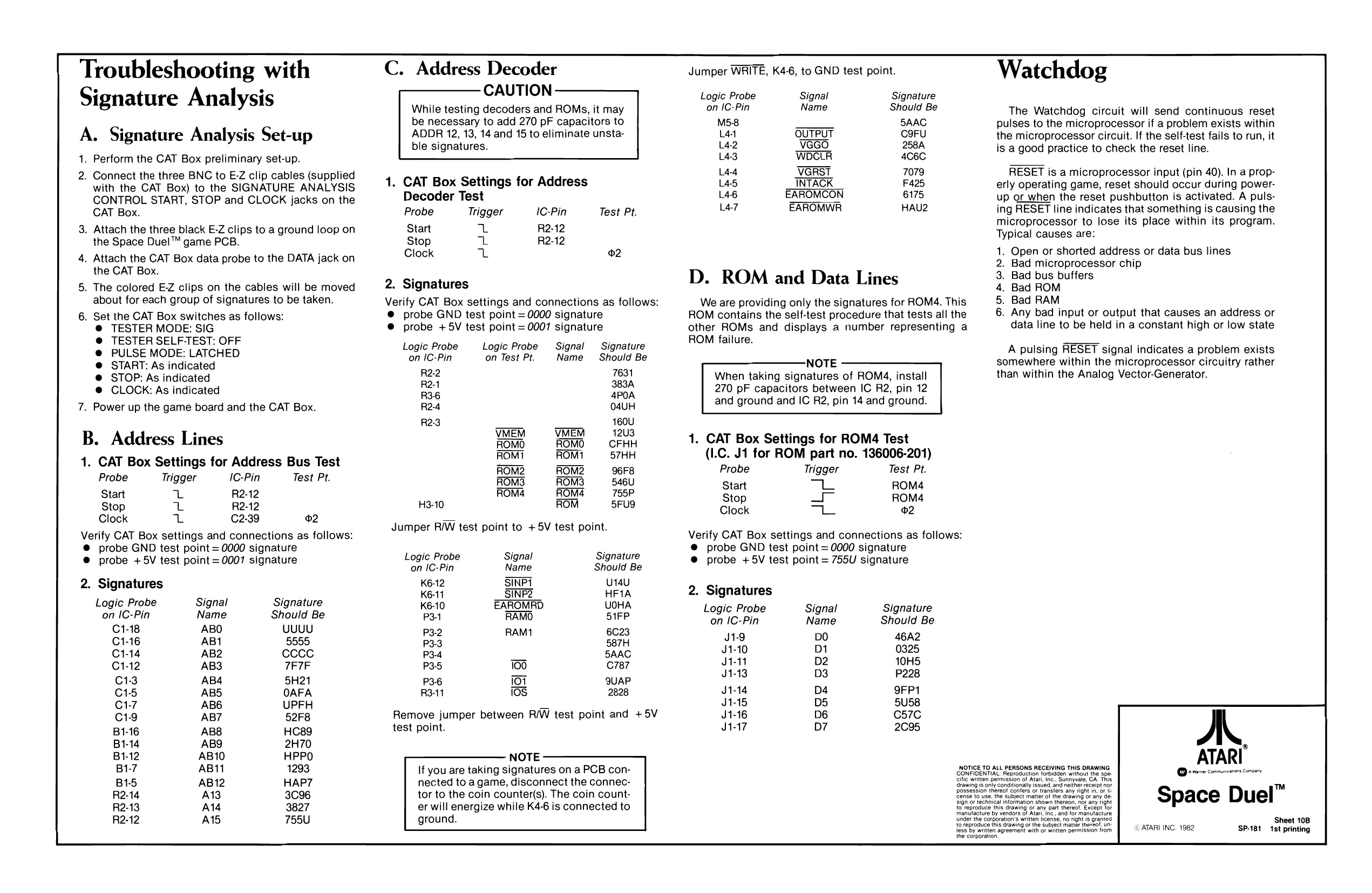
Troubleshooting with Signature Analysis
A. Signature Analysis Set-up
1, Perform the CAT Box preliminary set-up.
- Connect the three BNC to E-Z clip cables (supplied with the CAT Box) to the SIGNATURE ANALYSIS CONTROL START, STOP and CLOCK jacks on the CAT Box. . Attach the three black E-Z clips to a ground loop on the Space Duel™ game PCB. . Attach the CAT Box data probe to the DATA jack on the CAT Box. . The colored E-Z clips on the cables will be moved about for each group of signatures to be taken. . Set the CAT Box switches as follows: TESTER MODE: SIG TESTER SELF-TEST: OFF PULSE MODE: LATCHED START: As indicated STOP: As indicated CLOCK: As indicated
- Power up the game board and the CAT Box.
B. Address Lines
- CAT Box Settings for Address Bus Test
| Probe | Trigger | IC-Pin | Test Pt. |
| Start | L | R2-12 | |
| Stop | L | R2-12 | |
| Clock | L | C2-39 | 2 |
Verify CAT Box settings and connections as follows:
@ probe GND test point = 0000 signature
@ probe +5V test point = 0001 signature
- Signatures
Logic Probe Signal
on IC-Pin Name Should Be
| C1-18 | ABO | UUUU |
| C1-16 | ABI | 5555, |
| C1-14 | AB2 | CCCCc |
| C1-12 | AB3 | 7F7F |
| C1-3 | AB4 | 5H21 |
| C1-5 | ABS | OAFA |
| C1-7 | AB6 | UPFH |
| C19 | AB7 | 52F8 |
| B1-16 | AB8 | HC89 |
| B1-14 | ABQ | 2H70 |
| B1-12 | AB10 | HPPO |
| B1-7 | ABI | 1293 |
| B15 | AB12 | HAP7 |
| R2-14 | A13 | 3096 |
| R2-13 | A14 | 3827 |
| R2-12 | AIS | 755U |
Signature C. Address Decoder
. CAT Box Settings for Address Decoder Test Probe Trigger IC-Pin
| Start | 1 | R212 |
| Stop | 1 | R2-12 |
| Clock | L | 2 |
Test Pt.
- Signatures Verify CAT Box settings and connections as follows: © probe GND test point = 0000 signature @ probe +5V test point = 0001 signature
| Logic Probe | Logic Probe | ‘Signal | Signature |
| on IC-Pin | on Test Pt. | Name | Should Be |
R2.2 7631 R2-1 383A R36 4POA R2-4 04UH R23 160U 12U3 CFHH 57HH 96F8 546U ROM 755P H3-10 5FU9 Jumper RIW test point to + 5V test point.
Logic Probe Signature on IC-Pin Should Be K6-12 U14U K6-11 HFIA K6-10 UOHA P34 S1FP P3-2 6C23 P33 587H
| P34 | _ | SAAC |
P3-5 C787
| P36 | ior | QUAP |
| R3-11 | 10S | 2828 |
Remove jumper between R/W test point and test point.
| Logic Probe | Signal | Signature |
on IC-Pin Should Be M5-8 SAAC L441 C9FU L4-2 258A 14-3 4C6C L4-4 7079 Las F425 L46 EAROMCON 6175 L47 EAROMWR HAU2
D. ROM and Data Lines
We are providing only the signatures for ROM4. This ROM contains the self-test procedure that tests all the other ROMs and displays a number representing a ROM failure.
- CAT Box Settings for ROM4 Test (I.C. J1 for ROM part no. 136006-201)
| Probe | Trigger | Test Pt. |
| Start | lL | ROM4 |
| Stop | JS | ROM4 |
| Clock | oo | 2 |
Verify CAT Box settings and connections as follows:
@ probe +5V test point = 755U signature
- Signatures
| Logic Probe | Signal | Signature |
| on IC-Pin | Name | Should Be |
| J1-9 | DO | 46A2 |
| J1-10 | D1 | 0325 |
| J1-11 | D2 | 10H5 |
| J1-13 | D3 | P228 |
| J1-14 | D4 | QFP1 |
| J1-15 | DS | 5U58 |
| J1-16 | D6 | C57C |
| J1-17 | D7 | 2095 |
NOTICE TO ALL PERSONS RECEIVING THIS DRAWING CONFIDENTIAL: Reproduction forbidden without the spe: Watchdog
The Watchdog circuit will send continuous reset pulses to the microprocessor if a problem exists within the microprocessor circuit. If the self-test fails to run, it is a good practice to check the reset line.
RESET is a microprocessor input (pin 40). In a properly operating game, reset should occur during powerup or when the reset pushbutton is activated. A pulsing RESET line indicates that something is causing the microprocessor to lose its place within its program. Typical causes are: . Open or shorted address or data bus lines . Bad microprocessor chip . Bad bus buffers . Bad ROM . Bad RAM . Any bad input or output that causes an address or data line to be held in a constant high or low state
A pulsing RESET signal indicates a problem exists somewhere within the microprocessor circuitry rather than within the Analog Vector-Generator.
AL ATARI’ rere cornea amen Cific watten permission of Aan, Ine. Sunnyvale, CA. This Sawing 's only conditionally issued, and neither receipt nor possession thereat confers or transters any right in, oF Gense to use, the subject matter of the drawing or any de Sign oF technical information shown thereon, nor any right to reproduce this drawing or any part thereo!. Except for Space Duel” manutacture by vendors ot Atar Inc, and for manutacture Under the corporation's written license, no right is granted to reproduce this drawing of the subjeci matter thereo! UP less by whiten agreement with or witen permission from Sheet 10B SP-181 1st printing © ATARI INC, 1982 the corporation.