Solar Fox General Instructions and Schematics (M051-00982-A012)
Solar Fox (upright) (Bally Midway, 1981) · Schematics · 67 pages · 59 sections · original scan
This page is a drawing, shown as the original scan.
This page is a drawing, shown as the original scan.
This page is a drawing, shown as the original scan.
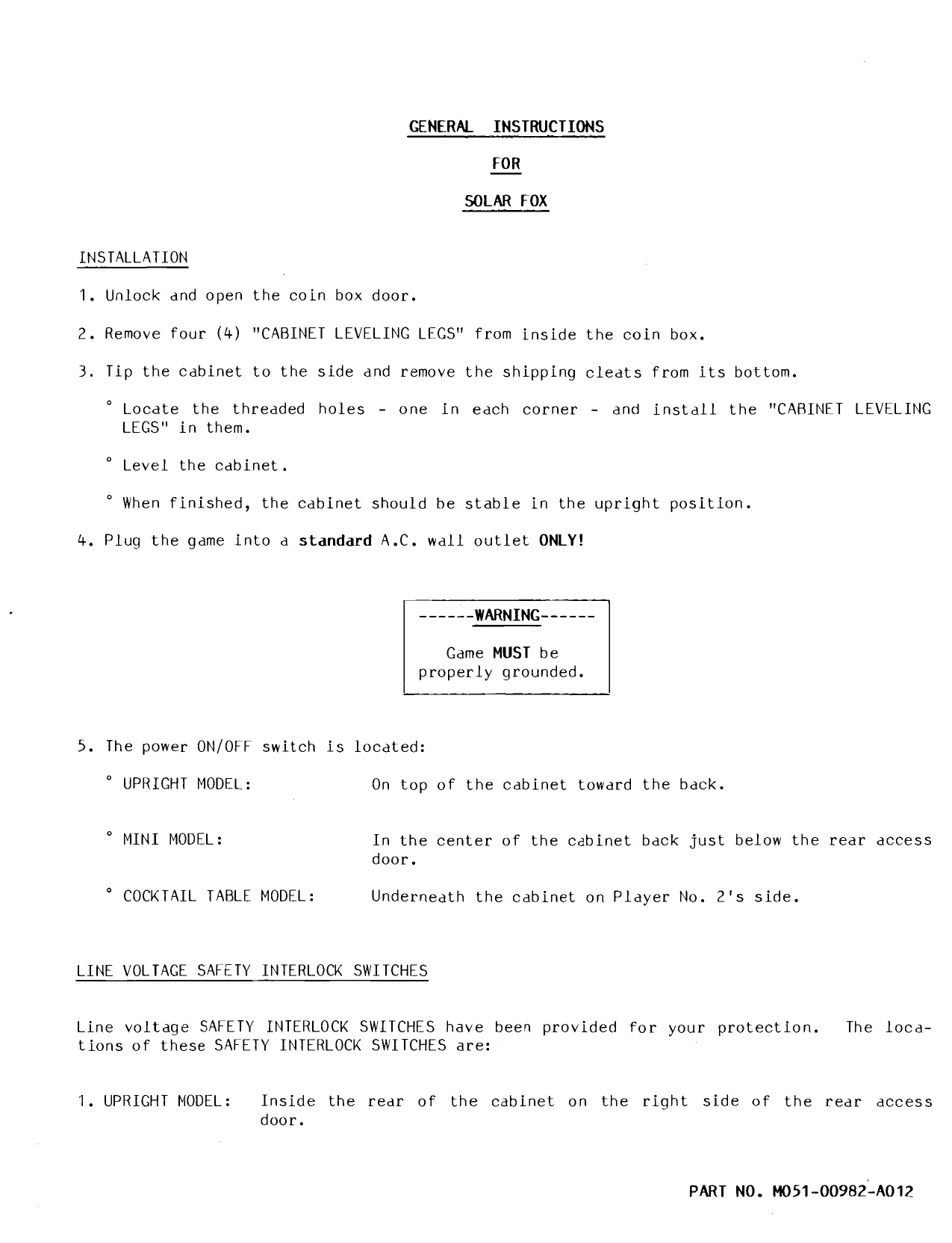
GENERAL INSTRUCTIONS
FOR
SOLAR _FOX
INSTALLATION
- Unlock and open the coin box door.
- Remove four (4) "CABINET LEVELING LEGS" from inside the coin box.
- Tip the cabinet to the side and remove the shipping cleats from its bottom.
° Locate the threaded holes - one in each corner - and install the "CABINET LEVELING LEGS" in them.
° Level the cabinet.
° When finished, the cabinet should be stable in the upright position.
4, Plug the game into a standard A.C. wall outlet ONLY!
Game MUST be properly grounded.
- The power ON/OFF switch is located:
° UPRIGHT MODEL: On top of the cabinet toward the back.
° MINI MODEL: In the center of the cabinet back just below the rear access door.
° COCKTAIL TABLE MODEL: Underneath the cabinet on Player No. 2's side.
LINE VOLTAGE SAFETY INTERLOCK SWITCHES
Line voltage SAFETY INTERLOCK SWITCHES have been provided for your protection. The locations of these SAFETY INTERLOCK SWITCHES are:
- UPRIGHT MODEL: Inside the rear of the cabinet on the right side of the rear access door.
PART NO. M051-00982-A012
~2-
2, MINI MODEL: Inside the rear of the cabinet on the right side of the rear access door.
- COCKTAIL TABEL: Inside the cabinet on the hinge side of the coin door.
When the cabinet access door(s) are secured in place, the SAFETY INTERLOCK SWITCH plunger(s) are in a fully depressed condition. The game circuit can function normally.
When any cabinet access door(s) are opened, the SAFETY INTERLOCK SWITCH plunger(s) are in a partially extended condition. This isolates the game circuit from the line voltage.
To restore power to the game circuit with the access door(s) open, gently pull the SAFETY INTERLOCK SWITCH plunger(s) out to the fully extended condition. THIS IS TO BE USED FOR SERVICING FHE GAME ONLY!
SELF-TEST
A slide switch is provided to make the game run a "Self-Test" on itself. The SELF-TEST SWITCH is located just inside the cabinet on the right side of the coin door frame as you face it.
To put the game into the Self-Test mode; turn the game ON and let it warm up for a few minutes. Then slide the SELF-TEST SWITCH to the ON position and actuate the "TILT" switch on the back side of the coin door just below the door lock to obtain the Self-Test-Menue dis-~ play on the monitor screen.
When in the Self-Test mode, the monitor screen will display the results of certain test functions the game has run on itself. (These will be discussed in more detail later.)
TO SERVICE THE CONTROL PANEL(S)
- UPRIGHT MODEL:
° The control panel is held in place by two latches, one on the left side and one on the right side of the cabinet.
They are spring loaded to provide constant positive pressure on their latch plates.
They can be reached through the coin door AFTER turning power to the game off.
To release the latches, lift up and toward the center of the control panel.
Once they are released, unhook them from their latch plates.
To remove the control panel:
Raise it up and tilt it toward you until you can see the cable behind it.
-~3-
Cradling the control panel between yourself and the cabinet, disconnect it from its cabling.
The control panel is now free and can be removed.
° To reinstall the control panel, reverse this procedure.
- MINI MODEL:
° The control panel is held in place by two latches, one on the left side and one on the right side of the cabinet.
They are spring loaded to provide constant positive pressure on their latch plates.
They can be reached through the coin door AFTER turning power to the game off.
To release the latches, Lift up and toward the center of the control panel.
Once they are released, unhook them from their latch plates.
To remove the control panel:
Raise it up and tilt it toward you until you can see the cable behind it.
Cradling the control panel between yourself and the cabinet, disconnect it from its cabling.
The control panel is now free and can be removed.
° To reinstall the control panel, reverse this procedure.
- COCKTAIL TABLE MODEL:
° Each control panel is held in place by several screws, two on the inside of the cabinet and three along the bottom edge of the control panel.
Turn the power off to the game.
Open the coin box door and release the two Latches on the inside of the cabinet up next to the table top.
Once they're released, unhook them from their latch plates.
Grasp the table top in the center above the coin door lifting up and to the side to tilt it open.
CAUTION: Due to the weight of the monitor,
the cabinet. REME CARE MUST be taken when opening
Remove the screws which secure the control panel in place.
° To remove the control panel(s):
Disconnect it from its cabling.
The control panel is now free and can be removed.
° To reinstall the control panel(s), reverse this procedure.
REMOVAL OF THE MAIN-DISPLAY-GLASS AND/OR THE T.V. BEZEL ASSEMBLY
1. UPRIGHT MODEL:
Turn the power to the game off and remove the control panel.
Remove the screws which secure the glass clamping plate.
Lift out the glass clamping plate. This frees the main-display-glass so it can be Lifted up.
By putting your finger in the hole in the middle of the main-display-glass support, you can lift it up and out.
Remove the screws which secure the T.V. bezel assembly in place (front and back).
The T.V. bezel assembly is now free and can be slid out of the cabinet.
To reinstall the T.V. bezel asssembly and the main-display-glass, reverse this procedure.
MINI MODEL:
Turn the power to the game off and remove the control panel.
Remove the screws which secure the glass clamping plate.
Lift out the glass clamping plate. This frees the main-display-glass so in can be lifted up.
By putting your finger in the hole in the middle of the main-display-glass support, you can lift it up and out.
Remove the screws which secure the T.V. bezel assembly and lift it out.
° Reverse this procedure to reinstall the T.V. bezel assembly and the main-display-alass.
- COCKTAIL TABLE MODEL:
° Remove the screws which secure the table top glass clamps in place.
Remove the table top glass.
Loosen the screws which secure the T.V. bezel-glass-clamps in place.
Move the clamps to the side and the bezel glass may be removed.
Remove the screws which secure the bezei assembly to the table top and the bezel with four bezel-glass-clamps may be removed.
To reinstall the T.V. bezel assembly and the table top glass, reverse this procedure.
VOLUME CONTROL POT
The volume control pot is located just inside the cabinet on the RIGHT side of the coin door frame. For adjustment, it may be reached through the coin door on ALL models,
To make the sounds louder, turn the pot clockwise (7%) as you face it.
To make the sounds less loud, turn the pot counterclockwise (47) as you face it.
VOLTAGE CONTROL POTS
The voltage control pots are located on the Linear Power Supply P. C. Board. They are preset at the factory and SHOULD NOT be tampered with at all unless the distributors service department is contacted first.
SELF-TEST
The Self-Test mode is a special mode for checking game play statistics as well as game switches and computer functions. It is the easiest and best way to check for proper operation of the entire game.
You may begin a Self-Test at any time by sliding the Self-Test switch to the "ON" position after the power to the game is on (Self-Test switch located just inside cabinet on right side of coin door frame). When this is done, the game will react as follows:
- If the game is in the Attract mode when the Self-Test switch is moved to the "ON" posi-
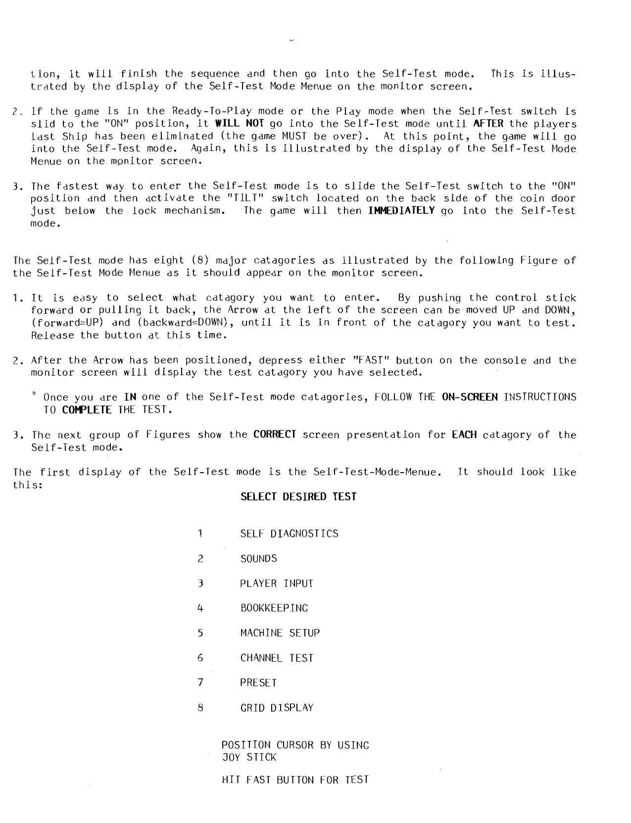
This page is a drawing, shown as the original scan.
~-7-
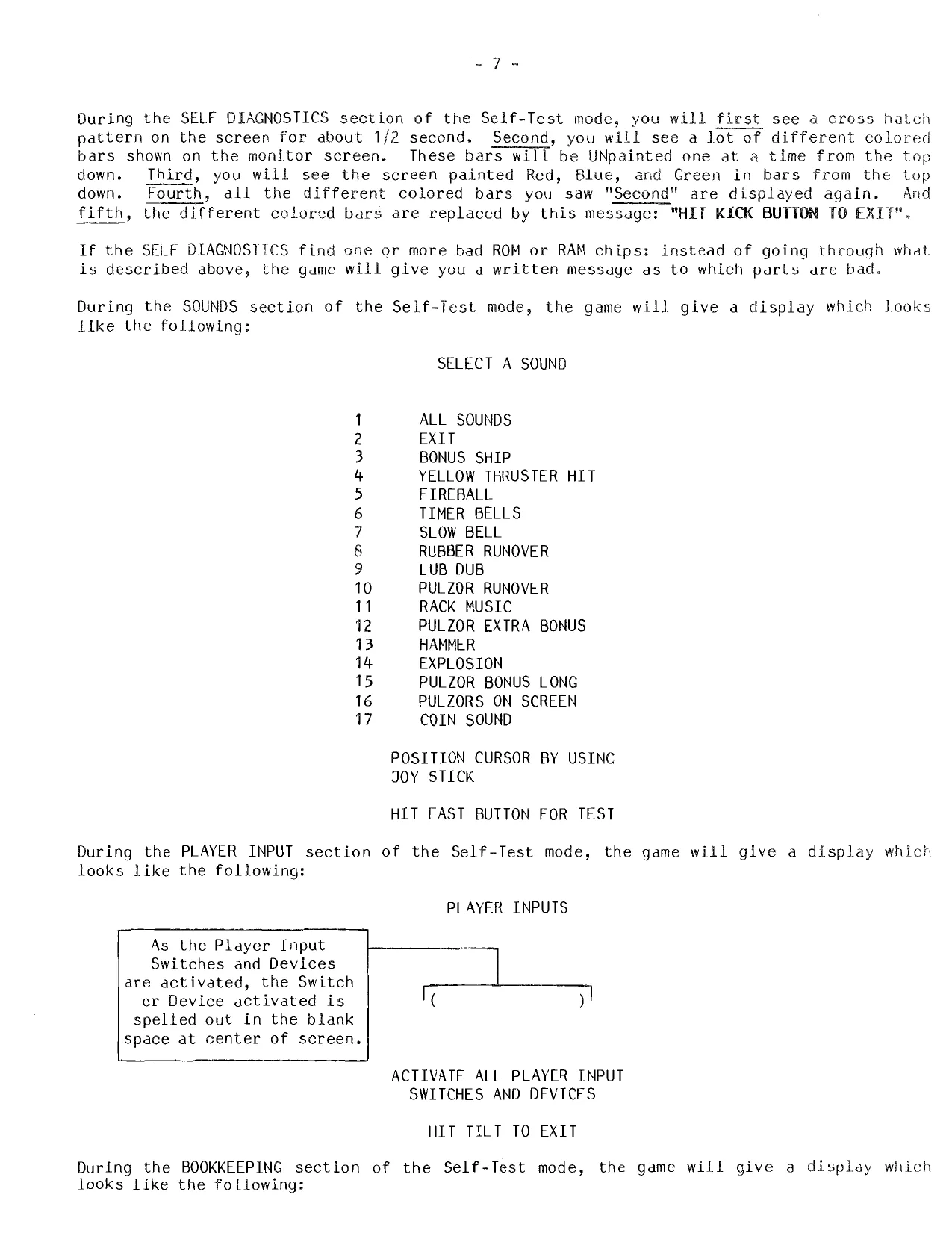
During the SELF DIAGNOSTICS section of the Self-Test mode, you will first see a cross hatch pattern on the screen for about 1/2 second. Second, you will see a lot of different colored bars shown on the monitor screen. These bars will be UNpainted one at a time from the top down. Third, you will see the screen painted Red, Blue, and Green in bars from the top down. Fourth, all the different colored bars you saw "Second" are displayed again. And fifth, the different colored bars are replaced by this message: "HIT KICK BUTTON TO EXIT".
If the SELF DIAGNOSTICS find one or more bad ROM or RAM chips: instead of going through what is described above, the game wili give you a written message as to which parts are bad.
During the SOUNDS section of the Self-Test mode, the game will give a display which looks Like the following:
SELECT A SOUND
ALL SOUNDS EXIT BONUS SHIP YELLOW THRUSTER HIT FIREBALL TIMER BELLS SLOW BELL RUBBER RUNOVER LUB DUB 10 PULZOR RUNOVER 11 RACK MUSIC i2 PULZOR EXTRA BONUS 13 HAMMER 14 EXPLOSION 15 PULZOR BONUS LONG 16 PULZORS ON SCREEN 17 COIN SOUND WDINAUFUN a>
POSITION CURSOR BY USING JOY STICK
HIT FAST BUTTON FOR TEST
During the PLAYER INPUT section of the Self-Test mode, the game will give a display which looks like the following:
PLAYER INPUTS
As the Player Input Switches and Devices are activated, the Switch or Device activated is spelled out in the blank space at center of screen.
ACTIVATE ALL PLAYER INPUT SWITCHES AND DEVICES
HIT TILT TO EXIT
During the BOOKKEEPING section of the Self-Test mode, the game will give a display which looks like the following:
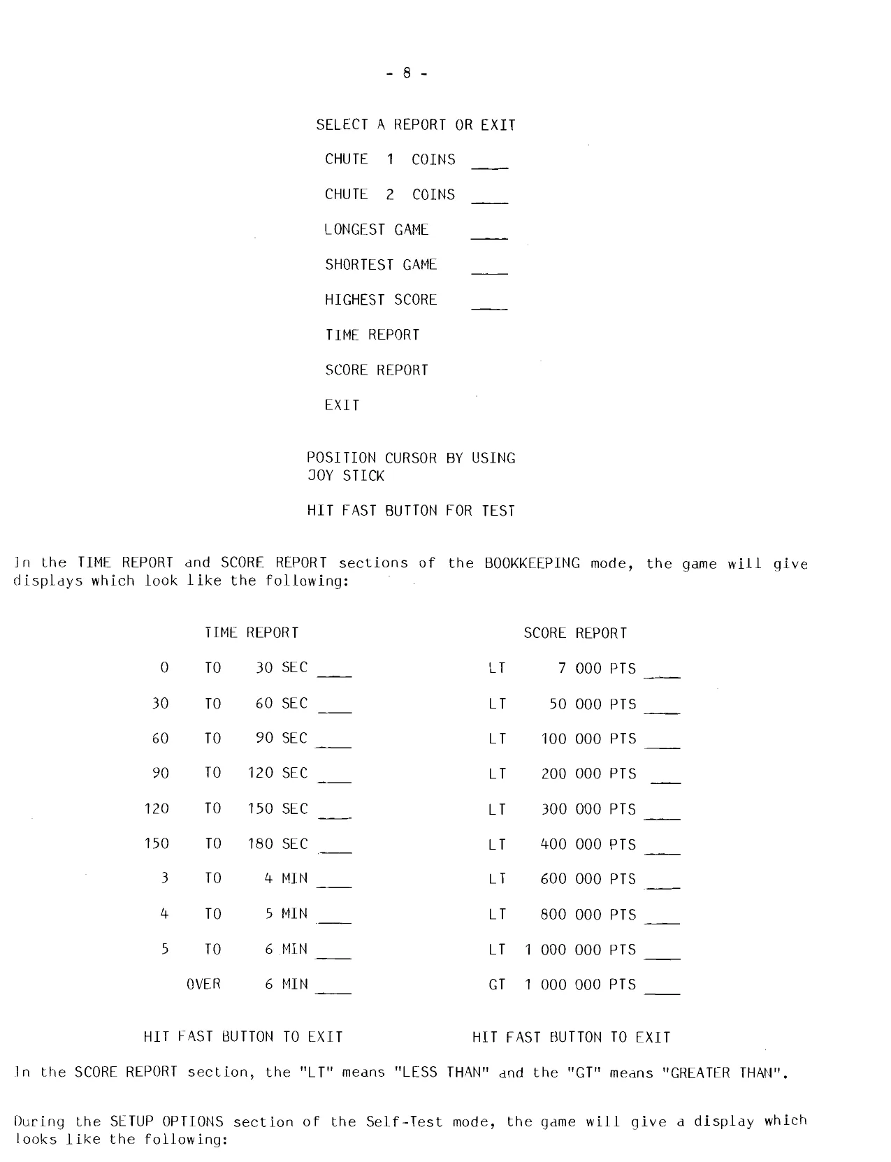
This page is a drawing, shown as the original scan.
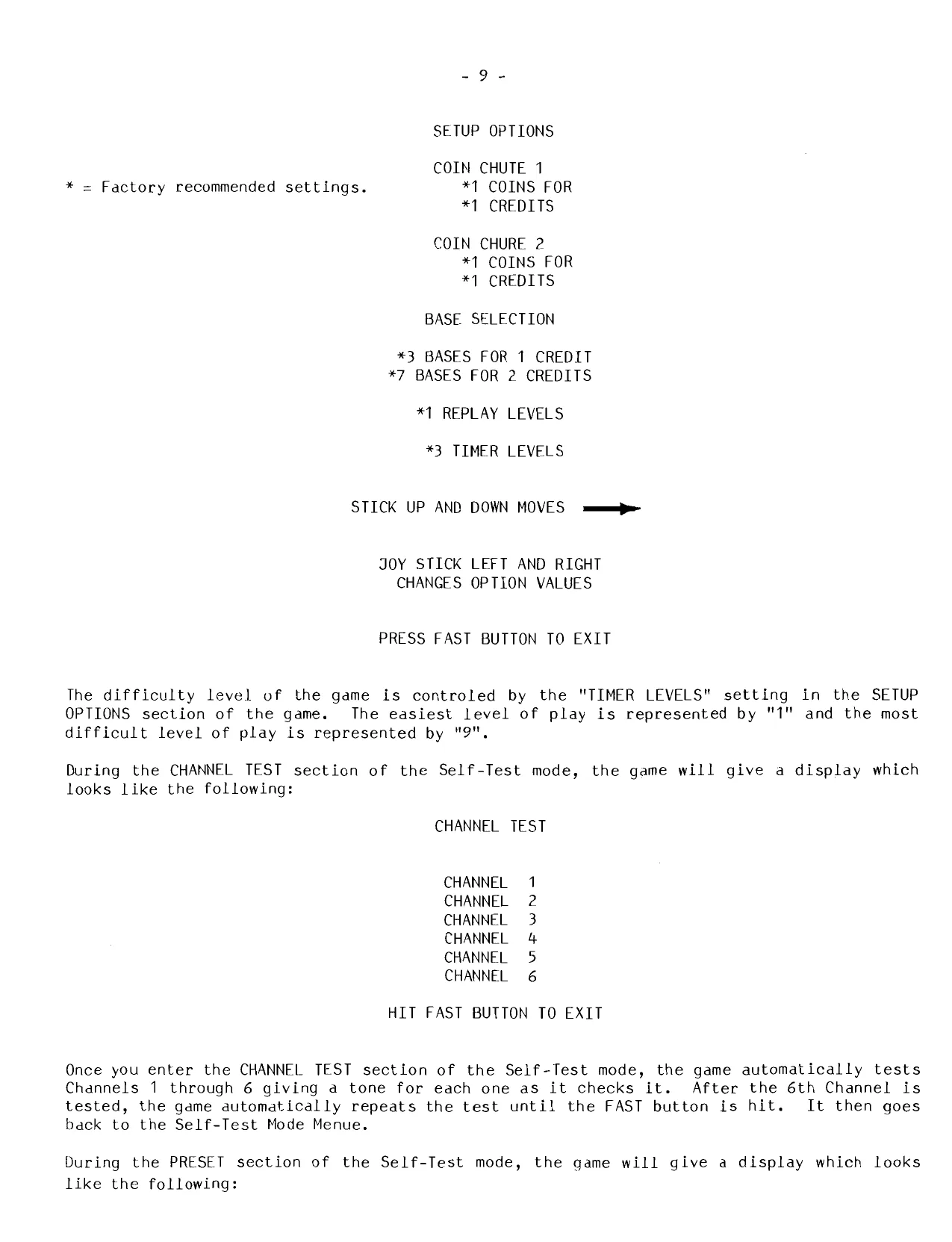
SETUP OPTIONS
COIN CHUTE 1
- = Factory recommended settings. *1 COINS FOR *1 CREDITS
COIN CHURE 2 *1 COINS FOR *1 CREDITS
BASE SELECTION
*3 BASES FOR 1 CREDIT *7 BASES FOR 2 CREDITS
*1 REPLAY LEVELS
*3 TIMER LEVELS
STICK UP AND DOWN MOVES ao
JOY STICK LEFT AND RIGHT CHANGES OPTION VALUES
PRESS FAST BUTTON TO EXIT
The difficulty level of the game is controled by the "TIMER LEVELS" setting in the SETUP OPTIONS section of the game. The easiest level of play is represented by "1" and the most difficult level of play is represented by "9".
During the CHANNEL TEST section of the Self-Test mode, the game will give a display which looks like the following:
CHANNEL TEST
CHANNEL CHANNEL CHANNEL CHANNEL CHANNEL CHANNEL DAUFWNA>
HIT FAST BUTTON TO EXIT
Once you enter the CHANNEL TEST section of the Self-Test mode, the game automatically tests Channels 1 through 6 giving a tone for each one as it checks it. After the 6th Channel is tested, the game automatically repeats the test until the FAST button is hit. It then goes back to the Self-Test Mode Menue.
During the PRESET section of the Self-Test mode, the game will give a display which Looks like the following:
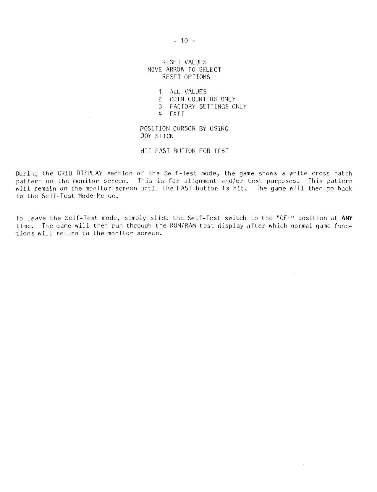
This page is a drawing, shown as the original scan.
SOLAR FOX
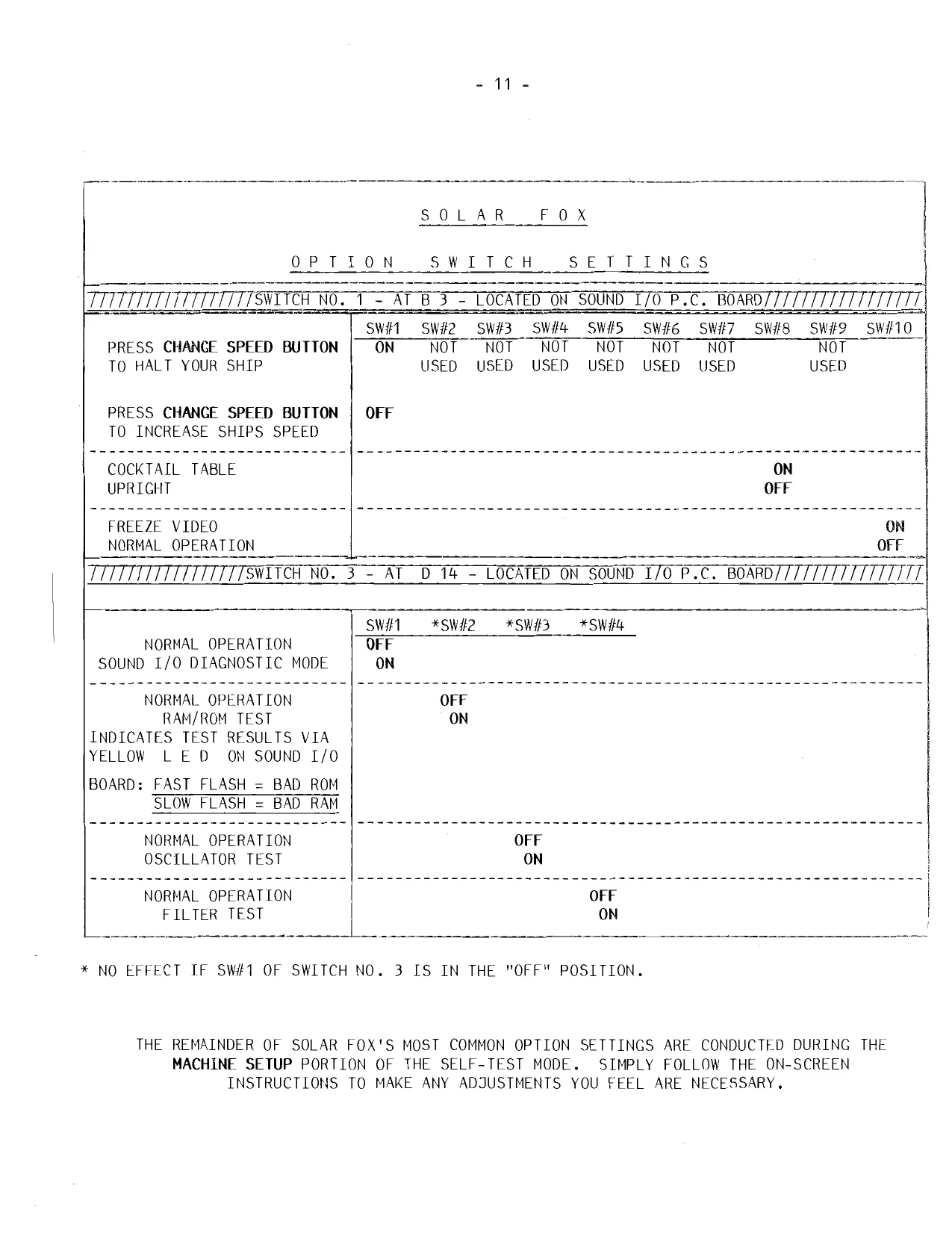
OPTION SWITCH SETTINGS \ TITTTTTTTT THT TTISHTTCH NO. 1 = AT B 3-= LOCATED ON SOUND 1/0 PC. BOARD/7777T7TTTTT TT i SW SWH2 _SWH3 SW WHS _SWi#6 _SNH7 SWS SW#9 _SWHT0 PRESS CHANCE SPEED BUTTON | ON NOT NOT NOT NOT NOT NOT NoT TO HALT YOUR SHIP USED USED USED USED USED USED USED
PRESS CHANGE SPEED BUTTON | OFF TO INCREASE SHIPS SPEED
COCKTAIL TABLE ON UPRIGHT OFF
FREEZE VIDEO ON NORMAL OPERATION _ OFF
NORMAL OPERATION SOUND 1/0 DIAGNOSTIC MODE
NORMAL OPERATION RAM/ROM TEST INDICATES TEST RESULTS VIA YELLOW LED ON SOUND I/0
BOARD: FAST FLASH = BAD ROM
SLOW FLASH = BAD RAM
NORMAL OPERATION OSCILLATOR TEST
NORMAL OPERATION FILTER TEST | Swi *swi2 *SWH3__ *SW4
OFF ON
ij OFF
- NO EFFECT IF SW#1 OF SWITCH NO. 3 IS IN THE "OFF" POSITION.
THE REMAINDER OF SOLAR FOX'S MOST COMMON OPTION SETTINGS ARE CONDUCTED DURING THE MACHINE SETUP PORTION OF THE SELF-TEST MODE. SIMPLY FOLLOW THE ON-SCREEN INSTRUCTIONS TO MAKE ANY ADJUSTMENTS YOU FEEL ARE NECESSARY,
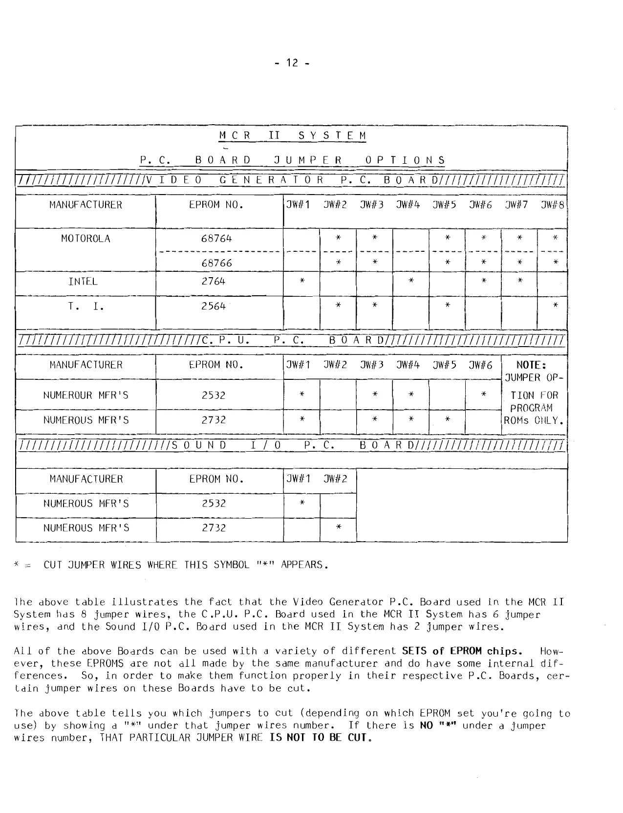
MCR II SYSTEM
| PoC. | BOARD | JUMPER | OPTIONS |
THT ATTTTTTNN TD EO GENERATOR P.-C. BOAR D/IIMMITTTIIT IT
| MANUFACTURER | EPROM NO. | JWT OWH2 WHS WHS OWES = WHEE WHT awe | |||
| MOTOROLA | 68764 | - | 7 | * | |
| 68766 | 4 | * | * | * | |
| INTEL | 2764 | * | 7 | * | 1 |
| | | I] | if" | |||
| TITTTTTTTITTTTTT TTT TIT TTTTIC. PU. | P. Cy | BOAR DITMTMUTITATTITITITNTTI | |||
| MANUF ACTURER | £PROM NO. | Iw#t IWH2 IWS WH WHS WHS | NOTE: |
Tp UHPER OP- *
| NUMEROUR MFR'S | 2532 | * | * | * | TION FOR |
|. PROGRAM
| NUMEROUS MFR'S | 2732 | # | | *. | + | * | ROMs CHLY. |
L. ——L—
| TTT is OUND | 170. | >. C. | BOAR DINTINITTTTTTT |
| MANUFACTURER | EPROM NO. | JWT IWik2 | |
| ~~ NUMEROUS MFR'S | 2532 | * |
=e
| NUMEROUS MFR'S | 2732 | x |
- = ami
- = CUT JUMPER WIRES WHERE THIS SYMBOL "*" APPEARS.
The above table illustrates the fact that the Video Generator P.C. Board used in the MCR IT System has 8 jumper wires, the C.P.U. P.C. Board used in the MCR IT System has 6 jumper wires, and the Sound I/0 P.C. Board used in the MCR II System has 2 jumper wires.
All of the above Boards can be used with a variety of different SETS of EPROM chips. However, these EPROMS are not all made by the same manufacturer and do have some internal differences. So, in order to make them function properly in their respective P.C. Boards, certain jumper wires on these Boards have to be cut.
The above table tells you which jumpers to cut (depending on which EPROM set you're going to use) by showing a "*" under that jumper wires number. If there is NO "*" under a jumper wires number, THAT PARTICULAR JUMPER WIRE IS NOT TO BE CUT.
This page is a drawing, shown as the original scan.
Harness Component Troubleshooting
Introduction
The most common problems occur in harness components such as the coin acceptor, player controls, interconnecting wiring, etc. The TV monitor and PCB computer cause their share of problems too, but not as much as the harness and its component parts. TV monitor troubleshooting will not be covered here because it is covered in that section of this manual. As you already know, the PCB computer is a complex device with a number of different circuits. Some circuits remain basically the same among games, but overall there area great many differences between them. PCB troubleshooting procedures, therefore, can be lengthy and will differ greatly among games. However, some basic Z-80 CPU information is involved in this section.
General Suggestions
The first step in any troubleshooting procedure is correctly identifying the malfunction’s symptoms. This includes not only the circuits or features malfunctioning, but also those still operational. A carefully trained eye will pick up other clues as well. For instance, a game in which the computer functions fail completely just after money was collected may have a quarter shorting the PCB traces. Often, an experienced troubleshooter will be able to spot the cause of the problem even before opening the cabinet.
After all the clues are carefully considered, the possible malfunctioning areas can be narrowed down to one or two good suspects. Those areas can be examined by a process of elimination until the cause of the malfunction is discovered.
Typical problems falling in this category are coin and credit problems, power problems and failure of individual features
5-1 NO GAME CREDIT For example, your prospective player inserts his quarter and is not awarded a game. The first item to check is if the quarter is returned. If the quarter is returned, the malfunction most certainly lies in the coin acceptor itself. First, use a set of test coins (both old and new) to ascertain that the player's coin is not undersize or underweight. If your test coins are also returned, coin acceptor servicing is indicated. Generally, the cause of this particular problem is a maladjusted magnet gate. Normally, this will mean slightly closing the magnet gate alittle by turning the adjusting screw out a bit (see section on coin acceptor for more details). If the quarter is not returned and there is no game credit, the cause of the malfunction may be in one of several areas. First try operating the coin return button; if the coin is returned, the problem is most likely in the magnet gate. Enlarge the gap according to the coin acceptor service procedures. If this does not cure the problem, remove the coin acceptor, clean it and perform the major adjustment procedure. lf the trapped coin is not returned when the wiper lever is actuated, you may have an acceptor jammed by a slug, gummed up with beer, a jammed coin chute, or mechanical failure of the acceptor mechanism. In this case, first check for the slug that will generally be trapped against the magnet. If so, simply remove the slug and test the acceptor. If the chute is blocked, remove the acceptor and remove the jammed coins. {f there is actual failure of the acceptor, remove the unit and repair as indicated in the coin acceptor service procedures. If the coin is making its way through the acceptor (that is, falling into the coin box), yet there is still no game credit, you either have a mechanical failure of the coin switch or electrical failure of the coin and credit circuits. The first place to begin is by checking the coin switch. Most of these switches are the make/break variety of micro switch, which is checked by testing for continuity between the NO, NC, and C terminals. When not actuated, the NC and C terminals should be continuous and the NO terminal open. When operated, the NO and C terminals should close and the NC should be open. If
the coin switch checks out, examine the connections
to the terminals to make sure there is good contact. If necessary, use the continuity tester and check from the terminal lug on the switch to the associated PCB trace. This will tell you if there is a continuous line all the way to the credit circuit.
If the coin switch wires do not check out, the problem is in the computer — most likely in the coin and credit circuitry. If you do get game credit when a coin is deposited, but the game will not start when the start switch is pressed, you may have a problem in the start switch, the interconnecting wiring or in the computer. First check the switch. If the switch is OK, proceed to check the wiring. Again, make sure you go from the terminal lug on the switch to the PCB trace. This way, you will check the terminal contact as well as PCB edge connector contact. If the wiring is continuous,
proceed to check the PCB credit circuit. If not, check
each section of the wiring, until the discontinuity is located. If the wiring is OK, the problem must lie in the computer.
Transformer and Line Voltage Problems
Your machine must have the correct line voltage to operate properly. If the line voltage drops too low, a circuit in the computer will disable game credit: The point at which the computer will fail to work will vary some from game to game, but no game will work on line voltage that drops below 105 VAC. Low line voltage may have many causes. Line voltage normally fluctuates a certain amount during the day as the total usage varies. Peak usage times occur mainly at dawn or dusk, so if your machine’s malfunction seems to be related to the time of day, this may be a factor. A large load connected to the same line as the game (such as a large air conditioner or other device with an exceptionally large motor) may drop the line voltage significantly when starting up. This drop can result in an intermittent credit problem. In addition, poor connections in the location wiring, plug, or line cord may also cause a significant drop in power. Cold solder joints in the game’s harness, especially in areas like the transformer connections, interlock switch, or fuse block, may also produce the same results, although probably on a more permanent basis. Sometimes location owners (especially in bars) replace light switches with dimmer rheostats, and the game is sometimes on the same line. Obviously, the voltage available to the game is going to drop dramatically when the dimmer is turned. In any case, the way to check for correct line voltage is with your VOM. Set the VOM to 250 VAC and stick the probes in the wall receptacle. If it's OK here, check the transformer primary connections. If you do not get 117 VAC, examine the solder joints on the transformer, fuse block, and interlock switch. If you do get 117 VAC, the problem must be either in the transformer, harness connections, or in the PCB power supply.
5-2 if you suspect the transformer, check its secondaries with the VOM set to 50 VAC and correlate the readings with the legend on the side of the transformer. The transformer must also be correctly grounded, so check the ground potential as well,
especially if there is a hum bar rolling up or down the
TV screen.
HARNESS PROBLEMS Other harness problems include blowing fuses and malfunctioning controls. The repeating blown-fuse problem can sometimes be quite exasperating to solve, for short circuits have the tendency to occur in areas almost impossible to find. First, try inserting a new fuse, as old fuses age and blow without cause. If the new one also blows, you definitely have a short. The best way to approach this problem is by turning the power off and disconnecting devices thatmay be causing the problem, such as the TV, transformer, and PCB. Disconnect the devices by pulling off their connectors, but do not allow them to touch. If necessary, insulate them with small pieces of electrical tape. Then, connect your VOM across the terminals of the fuse block (all electrical power shut off), and set it to one of the resistance scales. This will save blowing a fuse each time you want to check the circuit. If the VOM reveals that disconnecting the devices removed the short, reconnect the devices one by one until the short returns. The last device connected is the one that is at fault. If the VOM readsa short even after the devices are disconnected, the fault must lie in the harness itself, and only patient exploration will reveal its location. First, carefully examine all the wiring, looking for terminals that may be touching, metal objects such as coins shorting connections or burned insulation. If necessary, use the VOM to check each suspected wire. MALFUNCTIONING CONTROLS One of the most common problems here is a bad potentiometer. Typically, a bad pot will cause the image to jump asit reaches a certain point. The only cure for this one is to install a new pot. If a feature that is operated by a switch (for example, joysticks, foot pedals, control panei buttons) does not operate at all, check the switch with a VOM or continuity tester to verify its operation. If the switch does not check out, replace it. If the switch is OK, you should suspect the input to the switch from the PCB. In this case, get out the harness and logic schematics and check to see what kind of inputit is.
In many cases, the input will be +5 VDC. If so, use the
VOM to check its presence. Normally, the switch is used to pull a +5 VDC line LOW to GND or to pulla LOW line HIGH. If the PCB output is missing, check the wire length from the PCB. If you find the signal at the PCB trace, the wire length or conneciion is at fault. If not, begin exploring the PCB using the logic schematics.
A Glossary of Microprocessor Terms
MICROPROCESSOR — one or several microcircuits that perform the function of a computer's CPU. Sections of the circuit have arithmetic and comparative functions that perform computations and executive instructions. CPU — central-processing unit. A computing system’s “brain”, whose arithmetic, control and logic elements direct functions and perform computations. The microprocessor section of a microcomputer is on one chip or several chips. PROM — programmable read-only memory. User permanently sets binary on-off bits in each cell by selectively tusing or not fusing electrical links. Nonerasable. Used for low-volume applications.
EPROM — erasable, programmable, read-only memory. Can be erased by ultraviolet light bath, then reprogrammed. Frequently used during design and development to get programs debugged, then replaced by ROM for mass production. ROM — read-only memory. The program, or binary ~ On-Off bit pattern, is set into ROM during manufacture, usually as part of the last metal layer put onto the chip. Nonerasable. Typical ROM's contain up to 16,000 bits of data to serve as the microprocessor's basic instructions. RAM — random-access memory. Stores binary bits as electrical charges in transistor memory cells. Can be read or modified through the CPU. Stores input instructions and results. Erased when power is turned off. LSI — large scale integration. Formation of hundreds or thousands of so-called gate circuits on semiconductor chips. Very large scale integration (VLS) involves microcircuits with the greatest component density. MOS — metal-oxide semiconductor. A layered construction technique for integrated circuits that achieves high component densities. Variations in MOS chip structures create circuits with speed and low-power requirements, or other advantages (static will damage a MOS chip).
Introduction to the
Z-80 CPU
The term “microcomputer” has been used to describe virtually every type of small computing device designed within the last few years. This term has been applied to everything from simple “microprogrammed” controllers constructed out of TTL MSI up to low end minicomputers with a portion of the CPU constructed out of TTL LSI “bit slices.” However, the major impact of the LSI technology within the last few years has been with MOS LSI. With this
technology, it is possible to fabricate complete and
very powerful computer systems with only a few MOS LS! components. The Zilog 2-80 family of components can be configured with any type of standard semiconductor memory to generate computer systems with an extremely wide range of capabilities. For example, as few as two LSI circuits and three standard TTL MSI packages can be combined to form a simple controller. With additional memory and I/O devices a computer can be constructed with capabilities that only a minicomputer could previously deliver. New products using the MOS LSI microcomputer are being developed at an extraordinary rate. The Zilog Z-80 component set has been designed to fit into this market through the following factors:
- ‘The Z-80 is fully software compatible with the popular 8080A CPU.
- Existing designs can be easily converted to include the Z-80.
- The Z-80 component set is at present superior in both software and hardware capabilities to any other microcomputer system on the market today.
4. For increased throughput the Z80A operating ata
4 MHZ clock rate offers the user significant speed advantages. Microcomputer systems are extremely simple to construct using Z-80 components. Any such system consists of three parts: 1, CPU (Central Processing Unit)
- Memory
- Interface Circuits to peripheral devices The CPU is the heart of the system. Its function is to obtain instructions from the memory and perform the desired operations. The memory is used to contain instructions and in most cases data that is to be processed. For example, a typical instruction sequence may be to read data from a specific peripheral device, store it in a location in memory, check the parity and write it out to another peripheral device. Note that the Zilog component set includes the CPU and various general purpose 1/O device controllers, while a wide range of memory devices may be used from any source. Thus, all required components can be connected together in a very simple manner with virtually no other external logic.
This page is a drawing, shown as the original scan.
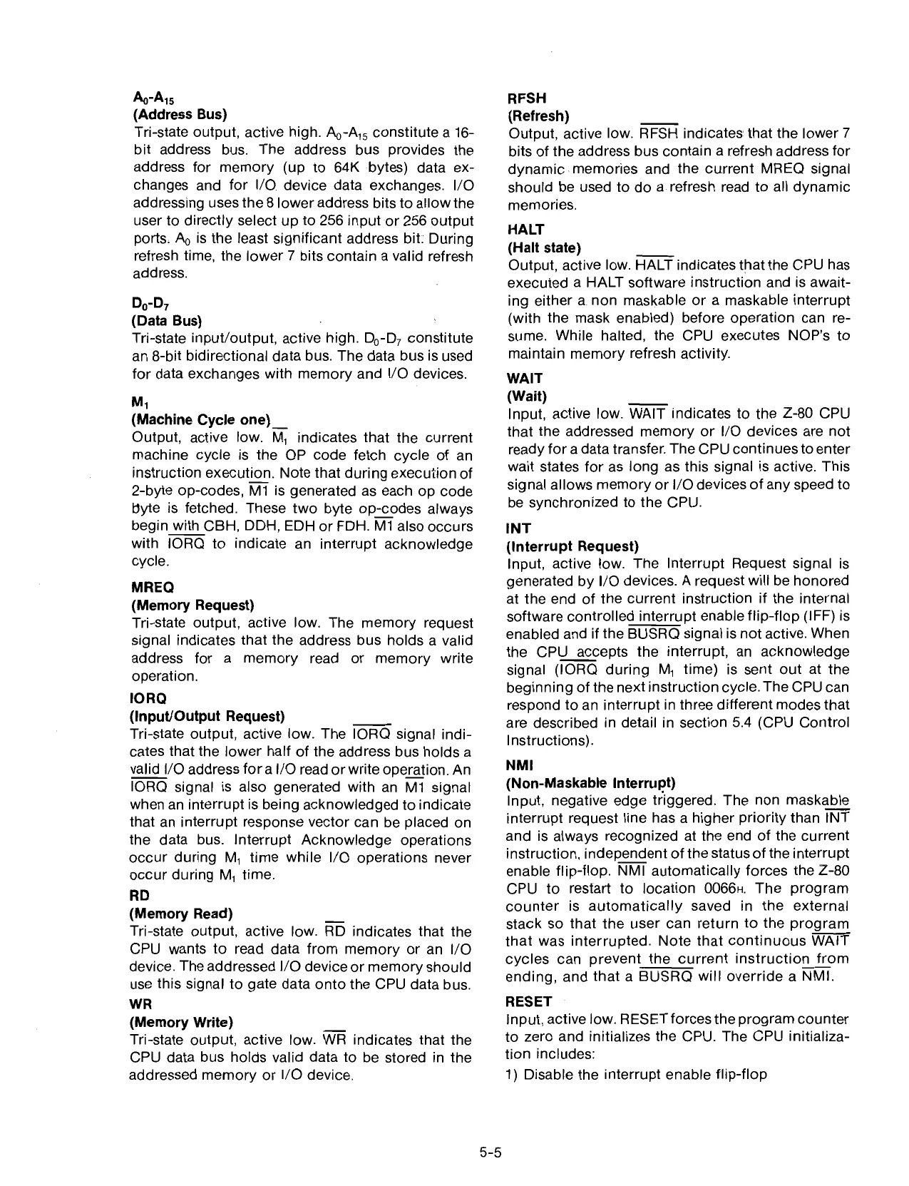
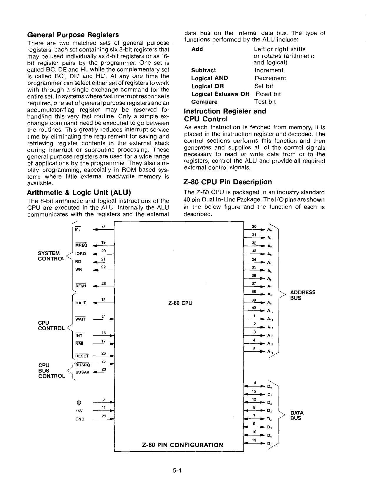
Ao-Ais (Address Bus) Tri-state output, active high. Ap-A,; constitute a 16bit address bus. The address bus provides the address for memory (up to 64K bytes) data exchanges and for \/O. device data exchanges. I/O addressing uses the 8 lower address bits to allow the user to directly select up to 256 input or 256 output ports. Ap is the least significant address bit: During refresh time, the lower 7 bits contain a valid refresh address.
Do-D; (Data Bus) Tri-state input/output, active high. Do-D; constitute an 8-bit bidirectional data bus. The data bus is used for data exchanges with memory and !/O devices.
M, (Machine Cycle one) __ Output, active low. M, indicates that the current machine cycle is the OP code fetch cycle of an instruction execution. Note that during execution of 2-byte op-codes, Mi is generated as each op code byte is fetched. These two byte op-codes always begin with CBH, DDH, EDH or FDH. Mi also occurs with IORQ to indicate an interrupt acknowledge cycle.
MREQ (Memory Request) Tri-state output, active low. The memory request
signal indicates that the address bus holds a valid
address for a memory read or memory write operation. 1oRQ (Input/Output Request) Tri-state output, active low. The ioRQ signal indicates that the lower half of the address bus holds a valid 1/O address fora I/O read or write operation. An IORQ signal is also generated with an M1 signal when an interrupt is being acknowledged to indicaie that an interrupt response vector can be placed on the data bus. Interrupt Acknowledge operations occur during M, time while I/O operations never occur during M, time. RD (Memory Read) Tri-state output, active low. RD indicates that the CPU wants to read data from memory or an I/O device. The addressed I/O device or memory should use this signal to gate data onto the CPU data bus. WR (Memory Write) Tri-state output, active low. WR indicates that the CPU data bus holds valid data to be stored in the addressed memory or I/O device.
5-5 RFSH (Refresh) Output, active low. RFSH indicates that the lower 7 bits of the address bus contain a refresh address for dynamic memories and the current MREQ signal should be used to do a refresh read to all dynamic memories.
HALT (Halt state) Output, active low. HALT indicates that the CPU has executed a HALT software instruction and is awaiting either a non maskable or a maskable interrupt (with the mask enabied) before operation can resume. While halted, the CPU executes NOP’s to maintain memory refresh activity.
WAIT (Wait) Input, active low. WATT indicates to the Z-80 CPU that the addressed memory or I/O devices are not ready for a data transfer. The CPU continues to enter wait states for as long as this signal is active. This signal allows memory or I/O devices of any speed to be synchronized to the CPU. INT (Interrupt Request) Input, active tow. The Interrupt Request signal is generated by I/O devices. A request will be honored at the end of the current instruction if the internal software controlled interrupt enable flip-flop (IFF) is enabled and if the BUSRQ signal is not active. When the CPU_accepts the interrupt, an acknowledge signal (IORQ during M, time) is sent out at the beginning of the next instruction cycle. The CPU can respond to an interrupt in three different modes that are described in detail in section 5.4 (CPU Control Instructions). NMI (Non-Maskable Interrupt)
Input, negative edge triggered. The non maskable
interrupt request line has a higher priority than INT and is always recognized at the end of the current instruction, independent of the status of the interrupt enable flip-flop. NMI automatically forces the Z-80 CPU to restart to location 00664. The program counter is automatically saved in the external stack so that the user can return to the program that was interrupted. Note that continuous WAT cycles can prevent _the current instruction from ending, and that a BUSRQ will override a NMI.
RESET forces the program counter jalizes the CPU. The CPU initializato zero and tion includes:
- Disable the interrupt enable flip-flop
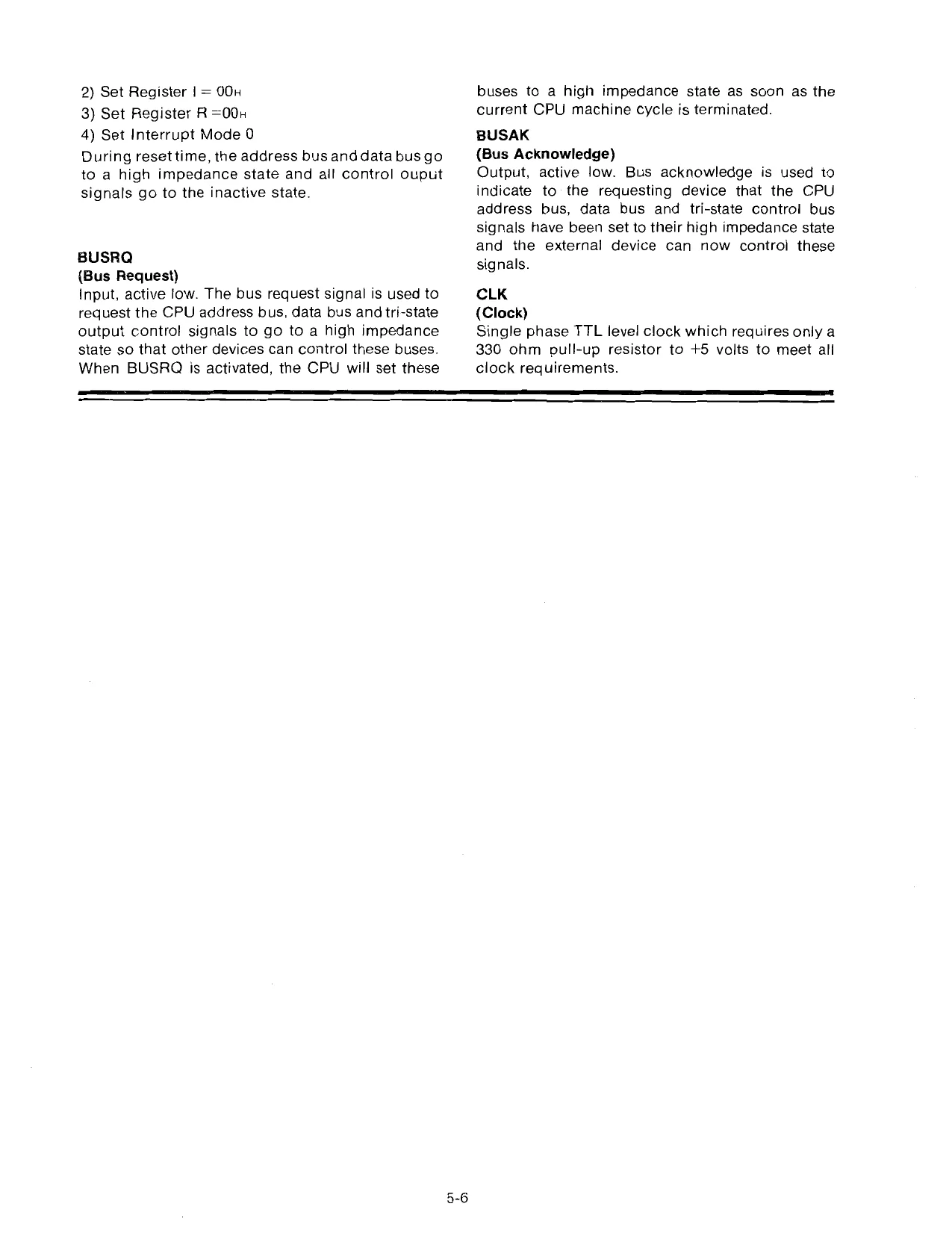
- Set Register | = 00H
- Set Register R =00u
- Set Interrupt Mode 0 During reset time, the address bus and data bus go to a high impedance state and all control ouput signals go to the inactive state.
BUSRQ (Bus Request) Input, active low. The bus request signal is used to request the CPU address bus, data bus and tri-state output control signals to go to a high impedance state so that other devices can control these buses. When BUSRQ is activated, the CPU will set these buses to a high impedance state as soon as the current CPU machine cycle is terminated. BUSAK (Bus Acknowledge) Output, active low. Bus acknowledge is used to indicate to the requesting device that the CPU address bus, data bus and tri-state control bus signals have been set to their high impedance state and the external device can now control these signals.
CLK (Clock) Single phase TTL level clock which requires only a 330 ohm pull-up resistor to +5 volts to meet all clock requirements.
This page is a drawing, shown as the original scan.
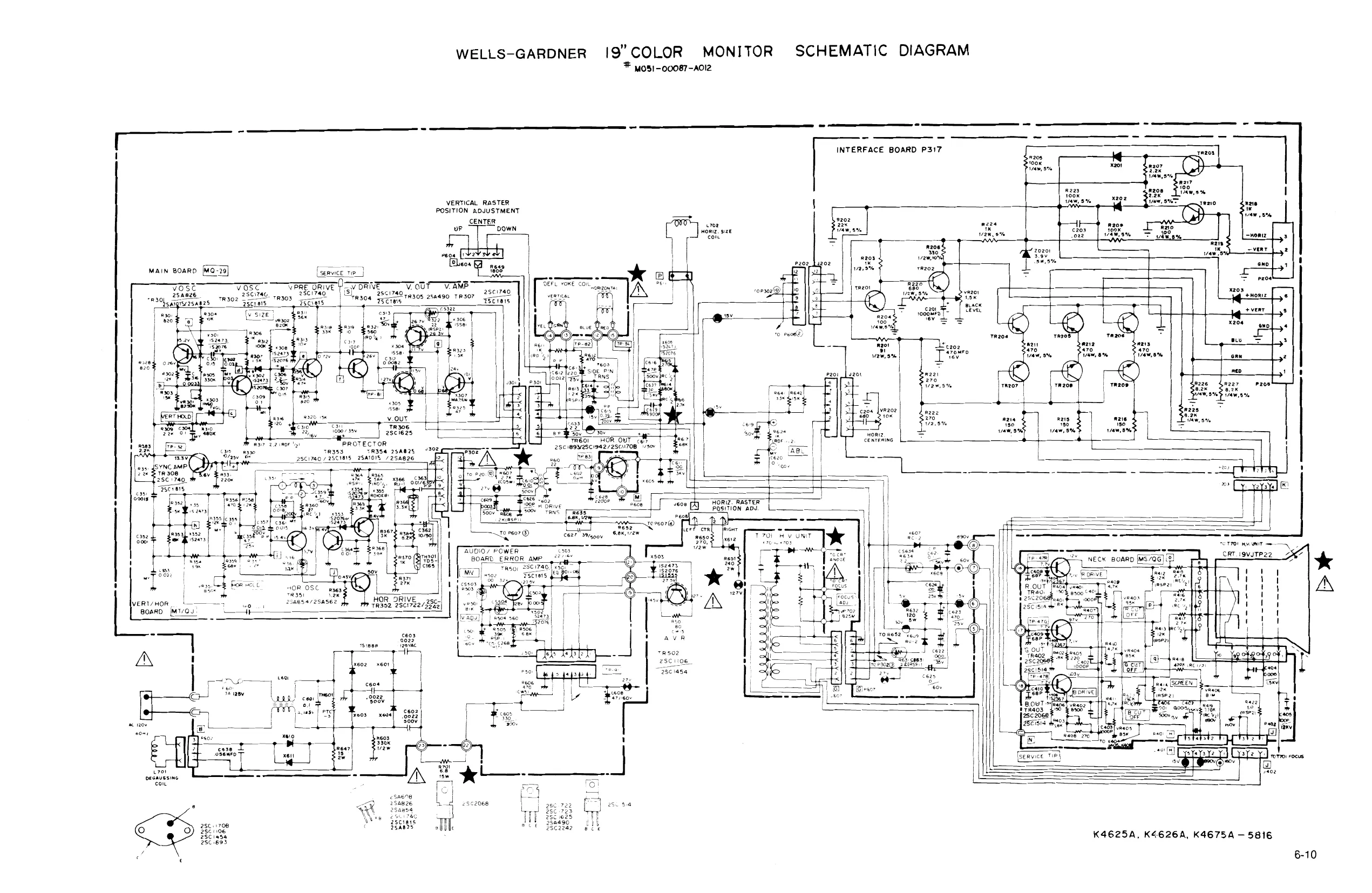
Color T.V.
Color T.V Monitor
Introduction: (How to use this section of your manual.)
This section has been designed to simply familiarize you with one of the more mystical components in your game — the T.V. monitor. If you are an electronics technician who is quite knowledgeable on the subject, you may decide to just go to the schematics and start troubleshooting the defective monitor. But if you are like most people, a monitor is a T.V. set, and that means a complex doo-dad that means big buck repairs. This isn’t necessarily so. This section of the manual will acquaint you with the monitor and could just help you repair it if you feel adventurous enough to give it a try. If you have any knowledge of electronics, especially the use of a voltmeter, the repairs you can make are astonishing. Just keep in mind that ELECTRICITY CAN BE VERY DANGEROUS, SO BE CAREFUL!!
If you want to understand how a monitor works, just read the “THEORY OF OPERATION” subsection. If you wish, you can follow along with the schematics. The information is presented in a very basic manner but more complete treatment of the subject can be found in the technical sections of bookstores.
lf you want to attempt to repair your monitor, it would be a good idea to read this whole section beginning to end before starting. Pay attention to all warnings
6-1 and take them seriously. The more equipment you have the better, but a low cost Volt-Ohm-Miiliameter can often do the trick. Here are the steps to take:
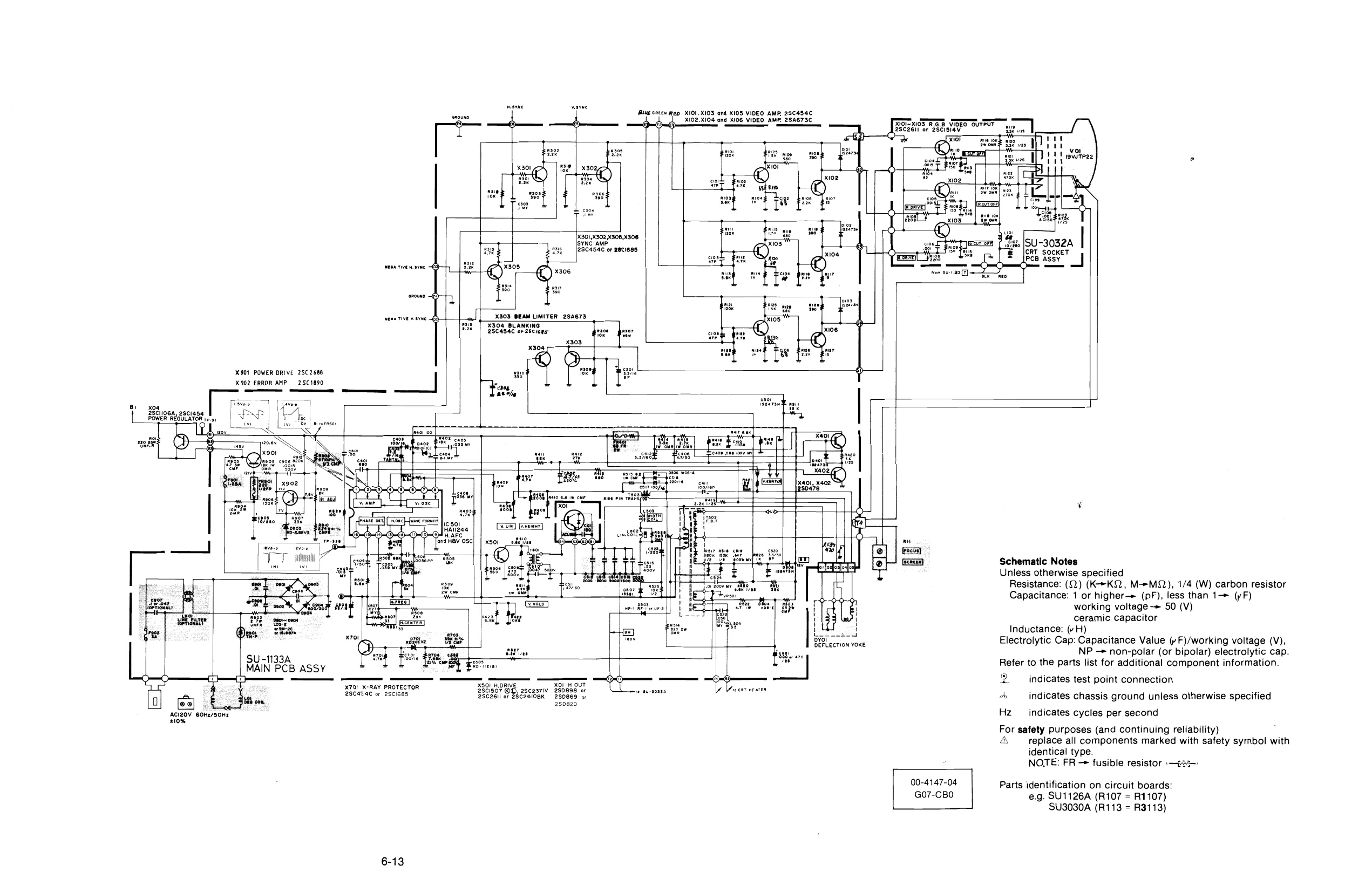
- Find the symptom that matches the problems your monitor has in the “SYSTEM — DIAG- NOSIS" subsection. The diagnosis tells the circuit or area the problem may be in and possibly even the actual component causing it. . Once you have the circuit that is causing the trouble, read the “TROUBLESHOOTING” subsection to learn the procedure for finding the bad part. Next, go to the schematic section and find the schematic that matches your monitor. It may be helpful to read the “DIFFERENCES BETWEEN MONITORS" subsection if you are unsure of which monitor you have. Use the schematic to see what parts are in the offending circuit.
That really is all there is to it. Just remember that there are some bizarre or rare symptoms not covered, or that a monitor may have two or more different problems that only a genius, the experienced, or an experienced genius can figure out. But be patient, follow safety precautions, and remember that there is also literature available from the monitor companies through your distributor or from Midway Manufacturing Company on request. (There is a toll
free number on the back side of the front cover of this
manual.)
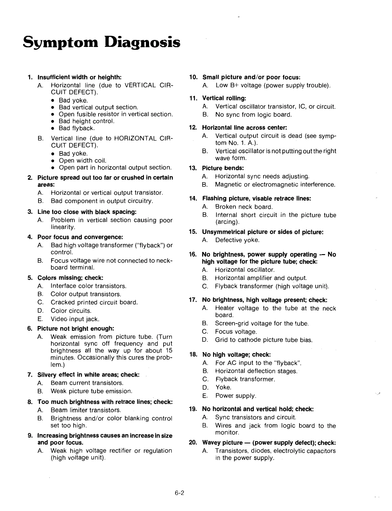
Symptom Diagnosis
. Insufficient width or heighth: A. Horizontal line (due to VERTICAL CIR- CUIT DEFECT). e@ Bad yoke. Bad vertical output section. e@ Open fusible resistor in vertical section. e Bad height control. © Bad flyback. B. Vertical line (due to HORIZONTAL CIR- CUIT DEFECT). e Bad yoke. e@ Open width coil. e Open part in horizontal output section. Picture spread out too far or crushed in certain areas: A. Horizontal or vertical output transistor. B. Bad component in output circuitry. . Line too close with black spacing: A. Problem in vertical section causing poor linearity. . Poor focus and convergence: A. Bad high voltage transformer (“flyback”) or control. B. Focus voltage wire not connected to neckboard terminal. . Colors missing; check: Interface color transistors. Color output transistors. Cracked printed circuit board. Color circuits. . Video input jack. . Picture not bright enough: A. Weak emission from picture tube. (Turn horizontal sync off frequency and put brightness all the way up for about 15 minutes. Occasionally this cures the problem.) . Silvery effect in white areas; check: A. Beam current transistors. B. Weak picture tube emission. moop>
. Too much brightness with retrace lines; check: A. Beam limiter transistors. B. Brightness and/or color blanking control set too high. . Increasing brightness causes an increase in size and poor focus. A. Weak high voltage rectifier or regulation (high voltage unit). 10.
11.
12.
13,
14,
15.
16.
17.
18.
19. Small picture and/or poor focus: A. Low B+ voltage (power suppiy trouble).
Vertical rolling: A. Vertical oscillator transistor, IC, or circuit. B. No sync from logic board.
Horizontal line across center: A. Vertical output circuit is dead (see symptom No. 1. A.). B. Vertical oscillator is not putting out the right wave form.
Picture bends: A. Horizontal sync needs adjusting. B. Magnetic or electromagnetic interference.
Flashing picture, visable retrace lines: A. Broken neck board. B. Internal short circuit in the picture tube (arcing). Unsymmetrical picture or sides of picture: A. Defective yoke.
No brightness, power supply operating — No high voltage for the picture tube; check: A. Horizontal oscillator. B. Horizontal amplifier and output. C. Flyback transformer (high voltage unit).
No brightness, high voltage present; check: A. Heater voltage to the tube at the neck board. B. Screen-grid voltage for the tube. C. Focus voltage. D. Grid to cathode picture tube bias.
No high voltage; check: For AC input to the “flyback”. Horizontal deflection stages. Flyback transformer. Yoke. Power supply. MOOD>
No horizontal and vertical hold; check: A. Sync transistors and circuit. B. Wires and jack from logic board to the monitor. Wavey picture — (power supply defect); check: A. Transistors, diodes, electrolytic capacitors in the power supply.
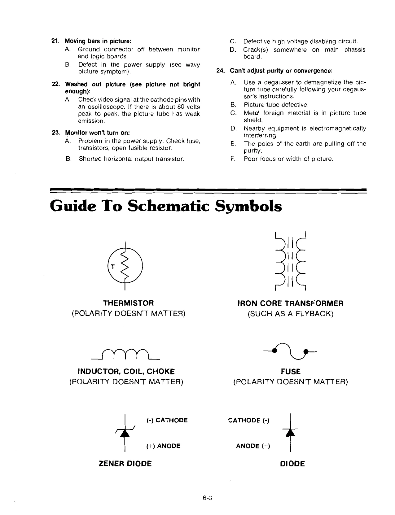
21.
22.
23. Moving bars in picture: A.
B. Ground connector off between monitor and logic boards. Defect in the power supply (see wavy picture symptom).
Washed out picture (see picture not bright enough): A. Check video signal at the cathode pins with an oscilloscope. If there is about 80 volts peak to peak, the picture tube has weak emission,
Monitor won't turn on: A. Problem in the power supply: Check fuse, transistors, open fusible resistor. B. Shorted horizontal output transistor. Cc. D. Defective high voltage disabiing circuit. Crack(s) somewhere on main chassis board.
- Can't adjust purity or convergence:
A.
B. Cc.
D.
m
™m Use a degausser to demagnetize the picture tube carefully following your degausser’s instructions. Picture tube defective. Meta! foreign material is in picture tube shield. Nearby equipment is electromagnetically interferring. The poles of the earth are pulling off the purity. Poor focus or width of picture.
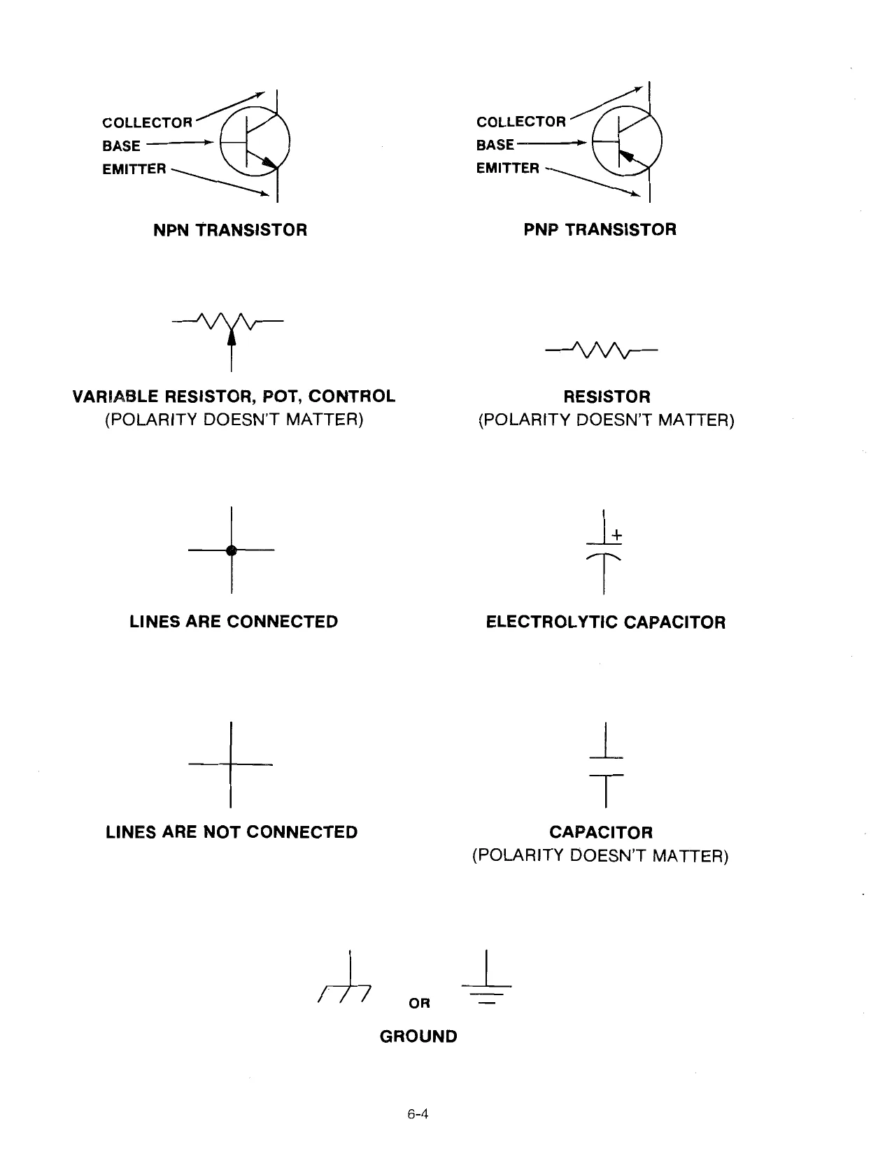
Guide To Schematic Symbols
THERMISTOR (POLARITY DOESN'T MATTER)
SY YW
INDUCTOR, COIL, CHOKE
(POLARITY DOESN'T MATTER)
(-) CATHODE
(+) ANODE
ZENER DIODE
6-3 IRON CORE TRANSFORMER (SUCH AS A FLYBACK)
OV
FUSE (POLARITY DOESN'T MATTER)
CATHODE (-)
ANODE (+)
DIODE
This page is a drawing, shown as the original scan.
Troubleshooting
Troubleshooting monitors requires experience, patience, and luck. The first step is to match the symptom the monitor displays to the diagnosis next to it in the “SYMPTOM-DIAGNOSIS” subsection. This will pinpoint the circuit the problem is probably in, and often the parts to check. Next, the circuit should be visually inspected to see if there are any parts broken, burned, or if something is there that shouldn't be, like a loose screw, etc. Some parts go bad before others and should be checked first. In fact, following is the general order in which parts usually go bad:
- Semiconductors (like transistors, diodes, and integrated circuits). Fusible resistors. Electrolytic capacitors, Resistors. Capacitors and coils. Always remember that a monitor can bite like a snake. Even when it is turned off, capacitors hold voltage and will discharge it to you should you be touching chassis ground. The picture tube or CRT, itself, is a giant capacitor, so avoid the flyback anode plug hole. With the monitor on, the power supply circuit and/or the flyback, which puts out at least 18,000 volts, CAN BE KILLERS! Avoid handling power transistors (usually output transistors), yoke terminals, and other hign power components when the monitor is on.
To maintain the safety and performance of the monitor, always use exact replacement parts. For instance, the wrong components in the power supply can cause a fire, or the wrong color transistor may give a funny color to the picture. Service your monitor on a nonconductive firm table like wood, NOT METAL, and take off all of your jewelry justin case. With all this in mind, you are ready to begin troubleshooting.
Observe the picture carefully. Try to vary the appropriate control that would most likely affect your particular symptom. For example, if there is poor brightness or no picture, try turning up the brightness or contrast control. If the controls have no effect at all, chances are there is trouble with the control itself, the circuit it controls, or a nearby circuit that
may be upsetting voltages. Go to the list of symptoms
and determine with the schematic where the bad circuit is.
Keep in mind that capacitors hold a charge as can the picture tube (for at least a week and usually longer), and could shock you.
First, check for obvious visual defects such as broken or frayed wires, solder where it is not supposed tobe, missing components. burned components, or cracked printed circuit boards. If everything looks good up to this point, make sure that diodes, electrolytic capacitors, and iransistors have their leads connected in the right polarity as shown on the schematic and the circuit board, Turn on the power and measure the voltages at the leads of the active devices such as tubes, transistors, or integrated circuits. Any voltage that does not come within at least 10% to 15% of the voltage specified on the schematic indicates either a problem with that device or acomponent connected with it in the circuit. The next step is to use the onmmeter to narrow down the field of possible offenders.
To test a transistor, one lead of the ohmmeter is placed on the base;-and the other lead placed just on the emitter, then on the collector. A normal transistor will read either high resistance (infinite), or littie resistance (400 to 900 ohms), depending on the polarity of this type transistor. Then the leads should be switched, one remaining on the base, and the other switched from the emitter to the collector. Now the opposite condition should result: the resistance should be infinite if it was lower when the other lead was on the base. Consistantly infinite readings indicate an open, and ashort is demonstrated by 0-30 ohms on most of these test readings. Finally, place one lead on the collector, then the other on the emitter. No matter which lead is used, there should be infinite resistance. Any lower reading, such as 50 ohms (which is typical on a bad transistor), indicates a short. This all sounds pretty confusing, but a little experience on a good transistor will make you an expert in no time. Usually, the lowest ohmmeter setting is used for testing transistors. Once in a great while a transistor may check out good on this test, but may actually be “leaky” or break down only on higher
voltages. If in doubt, change it. Itis also wise to check
the transistor out of the circuit just in case some component in the circuit is affecting the ohnmmeter reading. A diode is tested like a transistor except it only has two leads. Again, there should be high resistance one way and little resistance the other. If it tests bad, take one lead out of the circuit in case some component is messing up the ohmmeter reading.
Without special equipment, integrated circuits are checked by verifying the proper DC voltage on the pins and the correct AC wave form using an oscilliscope. BE CAREFUL: Shorting their pins can easily destroy them. Resistors are checked with an ohmeter and should usually be within ten percent of the value stated on them and on the schematic. You may have to desolder one lead from the printed circuit board. If you wreck the foil on the board, carefully solder a small wire over the break to reconnect the conductive foil. Capacitors are tricky. Their resistance goes up when checked with an ohmmeter which shows a charging action. As they suck up current from the meter, the voltage goes up and so does the resistance. Ityou are sure a particular circuit is giving you a problem and everything else checks out O.K., Electrolytic capacitors are prime suspects. Substitute a new one and keep your fingers crossed.
Theory of Operation
To understand what goes on inside the monitor, large general groups of circuits will be examined instead of laboriously analyzing the branches and small circuits that make up these groups. This will help avoid confusion and aid in a basic, concrete, knowledge of what makes up a monitor.
THE POWER SUPPLY — The AC going to the monitor from the game transformer is just like the voltage and current from your
wail outlet. lt jumps up and down going positive and
negative sixty times a second. But a monitor needs nice, smooth DC; direct current, not alternating. So
diodes chop up the AC and a big electrolytic
capacitor filters it out to make it even smoother. Since the monitor is a big piece of electronic equipment, with many circuits demanding a lot of power from the power supply, there are also zener diodes and transistors to help maintain a nice, constant, smooth voltage so that the monitor circuits don't jump around. And this is what happens when you see a wavy picture. There is AC creeping
6-6 through the power supply, so it must be malfunctioning. If the voltage from the power supply is too low, the other circuits will be starved for power and you may see a small, wavy picture, or none atall. Some circuits receive voltages that are higher than what the power supply should put out. But they come from the flyback transformer which will be discussed later.
THE INTERFACE SECTION OF THE CHASSIS — The interface section of the chassis is fairly easy to identify. It is right by the place where the video jack(s) from the logic board(s) plug into. There are sets of transistors that receive the separate red, green, blue, and sync information from the cables that come from the logic boards. The circuits jack up the voltage and match impedances, or in other words, prepare the logic board outputs for the circuits that will really amplify them for the output devices such as the yoke in the case of the sync, or the picture tube that shows the colors.
An interesting aside is that our sync is composite negative sync. That means two things:
- The sync is a negative going wave form.
- There are two pulses going at different speeds over the same wire: a. Vertical wave forms at 60 times per second (or Hertz) and b. Horizontal wave forms at about 15,750 times per second (Hz).
The sync is amplified by a sync amplifier transistor and sent on its wey to the oscillators. The sync or timing information wil! be explained along with the oscillator shortly The color information is sent via wires to the neck board where the main amplification occurs. This wilt also be discussed later.
VERTICAL AND HORIZONTAL DEFLECTION — After the sync signal is amplified by the sync amp, it goes to two different sections, the vertical and horizontal circuits. Basically, the sync signals are for timing so the picture doesn't mess up since it is assmebled like an orderly jigsaw puzzle, but so fast that you can't see ihe electron beams for each color painting the picture on the screen. This will all become clear soon. For now, we will follow the 60 cycle component of the sync as it goes onits journey to the deflection yoke. The 60 cycle pulse goes to the vertical oscillator to make sure this circuit goes back and forth (or oscillates) at 60 times a second. Without this pulse keeping the circuit at the correct speed, it may get lazy and oscillate at 58 cycles or lower, or get ambitious and oscillate at 62 cycles or higher. At the wrong speed, the picture will start to roll up or down. A Wells Gardner 13” or 19” color monitor uses transistors for its sync section. An Electrohome 13” or 19" color monitor uses an integrated circuit IC501 for its sync section. The idea is all the same. The output to the vertical amplitying transistors for all monitors must be a sawtooth wave form, sort of likea bunch ef pyramids, racing to the yoke’s vertical coils at 60 times a second. Along the way to the output transistors, the 60 cycle pulse is shaped and amplified to do the job: the yoke magnetically pushes the electron beam to fill the screen out sideways looking at the screen with the greatest length going up and down. Or viewing the screen sitting like a home television set. The amplified vertical output fills the screen up and down. Watching a monitor like this, seeing only ahorizontal line means a problem with the vertical coils of the yoke or anything from the vertical output section on back to the oscillator.
6-7 The horizontal section is very similar with a few exceptions. The horizontal wave shape is more like 4 square and has a frequency of 15,750 cycles a second. Again, Wells Gardner usestransistors for the horizontal oscillator, and Electrohome uses the other side of \C501. Still, the effect is the same. If the oscillator isn't going at the correct speed, the picture may move sideways, start to slant, or tear up with sianted thin figures. With both the vertical and horizontal of all monitors, there are variable resistors that change the speed of the oscillators up and down. This way you have controls that can make the correct frequencies to keep the electronic jigsaw puzzle nicely locked in place. \f you’re driving in a car and next to you someone else is driving their car at exactly the same speed, it will appear that they are not moving. And this is why the sync frequency and the osciliators frequencies must match, so the picture doesn't appear to move. The correct wave form is shaped and amplified in the circuitry just like in the vertical section. But the horizontal output transistor is a large power transistor and not only serves to give current to the horizontal yoke windings, it also feeds the flyback transformer.
THE FLYBACK TRANSFORMER (OR HIGH VOLTAGE UNIT)
HIGH VOLTAGE UNIT) — The picture tube needs high voltage to light up, and the power supply can’t meet this demand. The flyoback transformer receives current alternating at about 15,750 times per second from the horizontal output transistor. The “flyback” jacks up its input voltage and puts out a higher voitage alternating at the same speed. But, in your “flyback” there are diodes that chop up the alternating voltage to rake it asmooth DC output just like in the power supply. This is what goes through that thick red wire to your picture tube. THIS AREA HAS ABOUT 18,000 VOLTS ON IT AND IT CAN KILL YOU! The “flyback” may be dangerous, but it is also generous. It has extra output windings which give voltage to the heater pins of the picture tube, voltage for the vertical deflection circuits, and picture tube screen-grid voltage. So in a way, the high voltage “flyback” is like a second power supply.
COLOR CIRCUITS The color circuits are pretty straight forward. The signais go into the interface section where some amplification and impedance matching occurs. These circuits are pretty sparse and simple. Each color just has two transistors and a diode with some resistors and capacitors. From here, the AC color signal is sent by wires io the neck board. The color output circuits are on the neck board. The color signais going to the transistors are controlled by two variable resistors called drive controls. There only two, one for the red and one for the green. The
blue doesn’t have one. In the emitter part of each transistor is another variable resistor that is the cut off control. These controls vary the amount of amplified AC signal that goes to the cathodes of the picture tube. The more signal, the more color. The bases of each of these transistors are connected together and are all connected to the blanking and beam iimiting transistors which are in the interface section. The beam limiter helps control the brightness level, and the blanking transistor rapidly turns the picture tube on and off so that retrace tines don’tshow up on the screen. By turning up the brightness on a good monitor, these four to six retrace lines can be seen slanting diagonally across the picture.
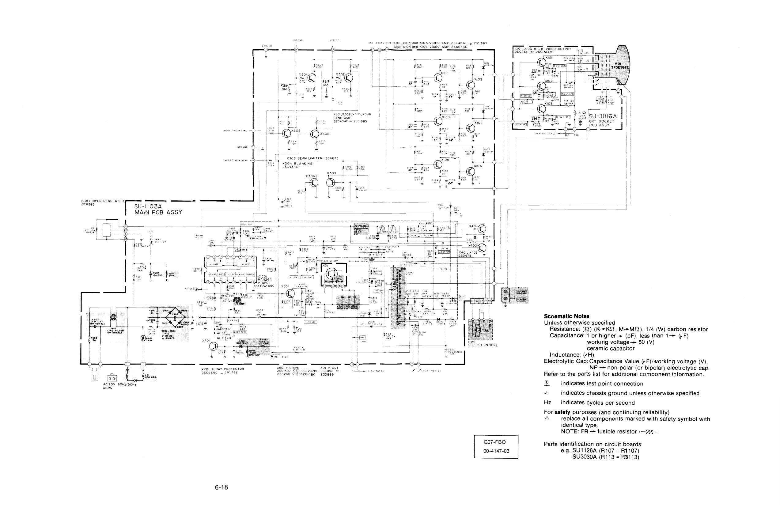
PROTECTION CIRCUIT — To protect the high voltage section against voltages that are too high coming from the power supply which could cause X-rays to be emitted from the “flyback”, a circuit senses the higher power supply voltage, and using a transistor, turns off the horizontal oscillator. Since the horizontal oscillator doesn’t work, the horizontal output transistor has nothing to feed the “flyback” which in turn has nothing to feed the picture tube. The monitor will be silent, have no picture, and will appear to be off. But don’t be fooled, There is still that excessive amount of voltage coming from the power supply. To find out, check ihe emitter on TR502 of the Wells Gardner monitors; or the emitter of X04 for the Electrohome monitor. Here are the voltages you should receive: Wells Gardner = 127VDC Electrohome = 120VDC
The best place to measure this voltage on an Electrohome monitor is at a pin marked B1 on the chassis. This is because a 13 inch color Electrohome monitor, the GO7-FBO or G07-902, has an integrated circuit and very little else in the power supply. Still, there should be 120VDC at B1.
THE PICTURE TUBE (OR CRT) — The picture tube or CRT is an output device. In other words, the end result of the circuits work is displayed by this part. Actually, the output of other circuits is in the neck of the picture tube. First, there_is the heater. The heater boils off electrons from the cathodes so that they (the electrons) shoot up to the screen to excite the phosphors so that the three phosphors emit three colors of light. The cathodes are next, and again they emit electrons to turn on the tube phosphors, making it glow. The cathode can arc or short to the heater resulting in no picture and a defective picture tube. Next come the grids. The first grid is grounded. The following grid is the screen grid which receives about 300VDC depending on the brightness setting. The next grid closest to the picture tube screen is the focus grid which gets about one fifth the amount of voltage that is applied to the picture tube anode. After jetting from the cathode through all these grids, the electrons speed through a mask, a sheet of material with tiny holes, and then excite the tiny dots of phosphor in the inside surface of the picture tube screen. The green electron gun (or cathode and circuitry) spits out electrons which head for the green phosphors only. The same goes for the red and blue guns. The way the phosphor light blends determines the color seen. Should these electron beams become too intense, they may burn the phosphor. With the monitor off, this can be seen as a dark permanent image of the video information on the tube screen.
Differences Between Monitors
The easiest way to identify the brand of monitor you are working with, assuming you can’t find the brand name written on it anywhere, is to see if there are two circuit boards rising up from the chassis toward the picture tube neck. In other words, they stand up, or are perpendicular to the chassis, with a black plastic bracket holding them in place. This is a description of a Wells Gardner monitor. They use separate boards for main chunks of circuitry. Therefore, you have a “power board” (the power supply), an “interface board” (the interface section), and a “horizontal/ vertical board” (for the deflection circuitry). Still, there are a few parts on the chassis, but most can be found on the board. An Electrohome monitor has no separate boards, except for the neck board, and just has a flat chassis.
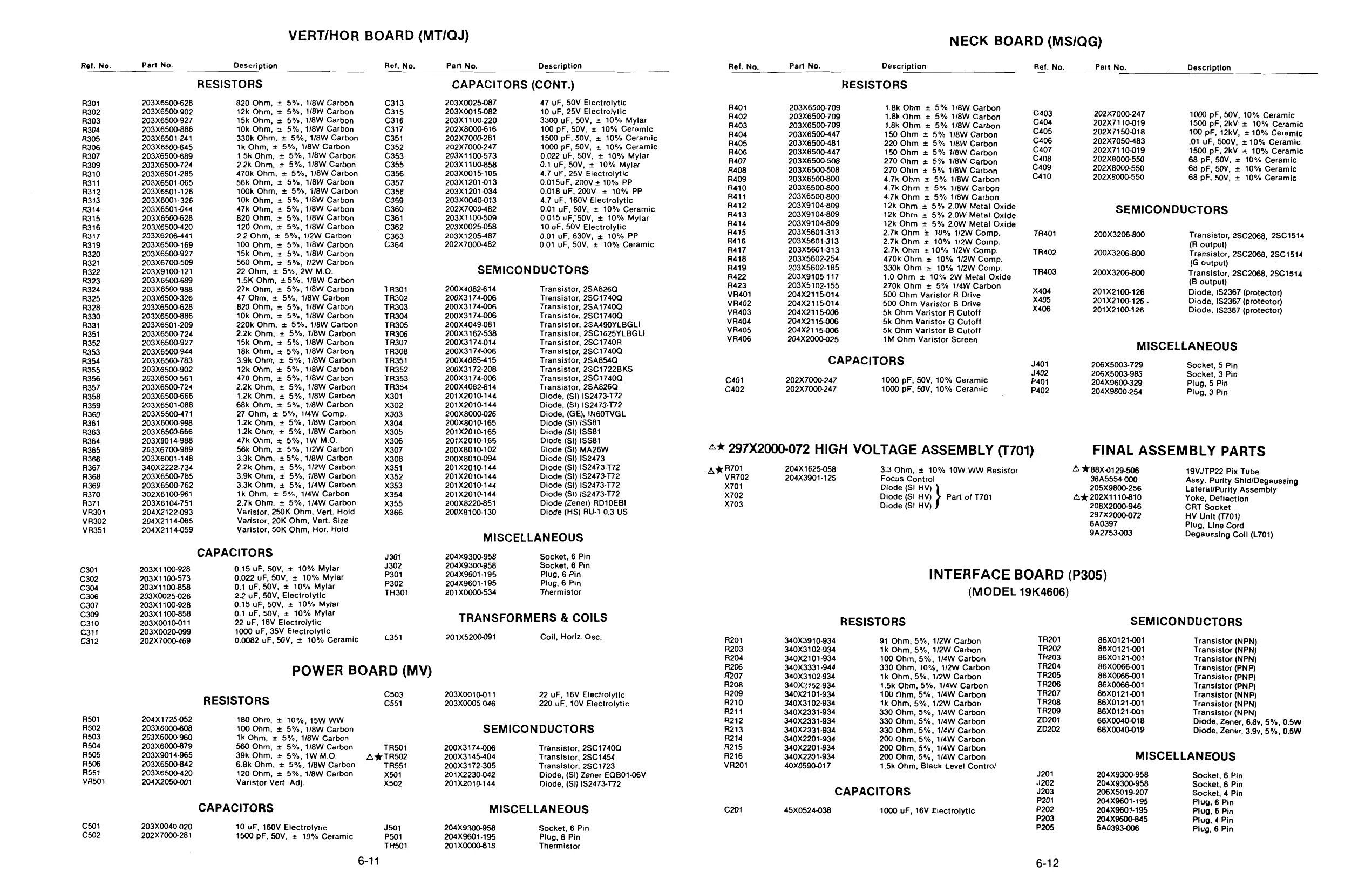
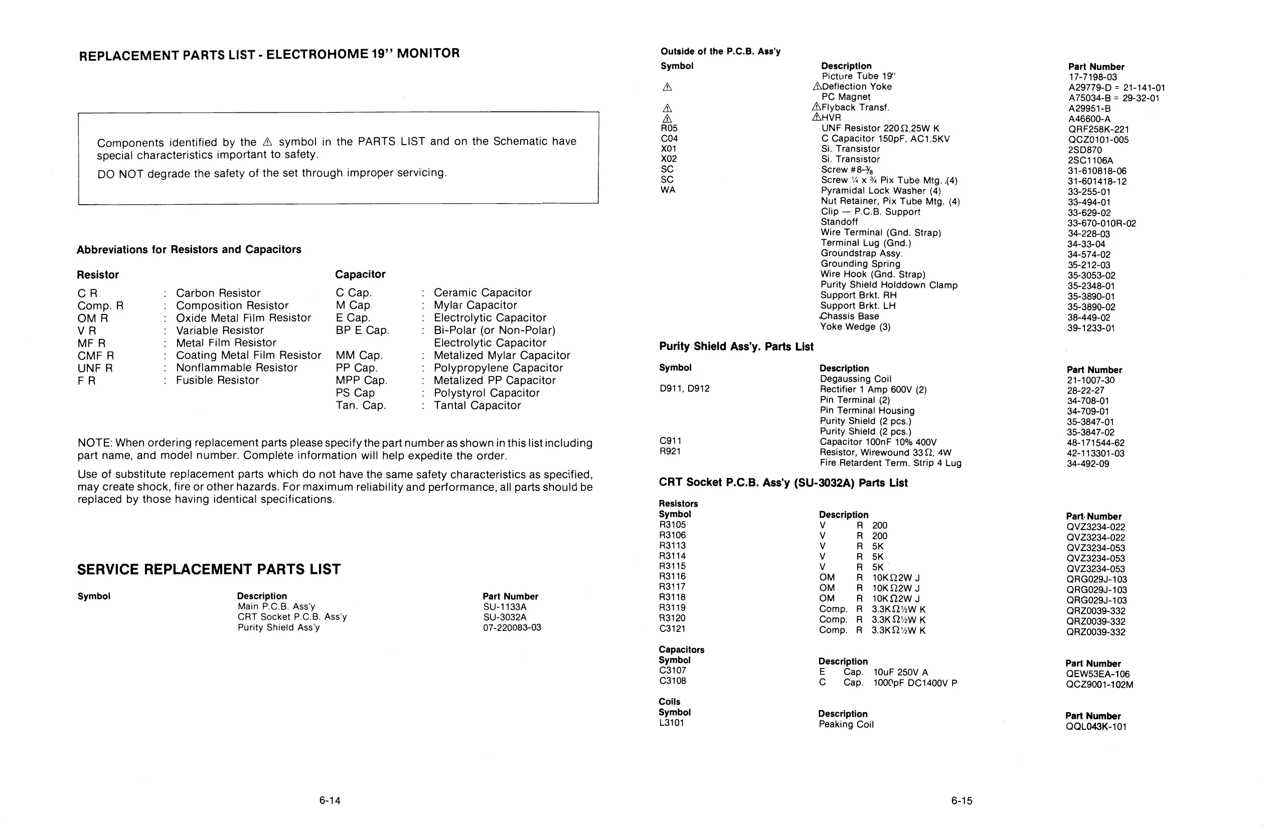
Another good way to determine which monitor you have is to check the transistor call out numbers that are printed on the chassis next to the part. For instance, on the neck board, one of the color output transistors is TR401. If you look through the schematics or the parts lists, you will find TR401 in the Wells Gardner literature. On the other hand, the neck board transistor may say X101. X101 can be found in the Electrohome literature. So, ail Wells Gardner transistor call outs begin with TR, and Electrohome transistor call outs start with an “Xx”.
This page is a drawing, shown as the original scan.
This page is a drawing, shown as the original scan.
VERT/HOR BOARD (MT/QJ)
| Rel. No. | Part No. | Description | Ret. No. | Part No. | Description |
RESISTORS CAPACITORS (CONT.)
| R301 | 203X6500-628 | 820 Ohm, + 5%, 1/8W Carbon | C313 | 203X0025-087 | 47 uF, SOV Electrolytic | ||
| R302 | 203X6500-902 | 12k Ohm, * 5%, 1/BW Carbon | C315 | 203X0015-082 | 10 uF, 25V Electrolytic | ||
| R303 | 203X6500.927 | 15k Ohm, + 5%, 1/8W Carbon | C316 | 203X1100-220 | 3300 UF, 50V, + 10% Mylar | ||
| R304 | 203X6500-886 | 10k Ohm, = 5%, 1/8W Carbon | 317 | 202X8000-676 | 100 pF, 50V, * 10% Ceramic | ||
| 305 | 203X6501-241 | 330k Ohm, + 5%, 1/8W Carbon | C351 | 202X7000-281 | 1500 pF, 50V, + 10% Ceramic | ||
| 306 | 203X6500-645, | 1k Ohm, * 5%, | 1/8W Carbon | C352 | 202X7000-247 | 1000 pF, 50V, + 10% Ceramic | |
| R307 | 203x6500-689 | 1.5k Ohm, + 5%, | 1/8W Carbon | C353 | 203X1100-573 | 0.022 uF, 50V, + 10% Mylar | |
| R309 | 203X6500-724 | 22k Ohm, + 5%, | 1/8W Carbon | C355 | 203X1100-858 | 0.1 uF, 50V, + 10% Mylar | |
| R310 | 203X6501-285 | 470k Ohm, + 5%, 1/8W Carbon | C356 | 203X0015-105 | 4.7 UF, 25V Electrolytic | ||
| R311 | 203X6501-065 | 56k Ohm, + 5%, | 1/8W Carbon | C357 | 203X1201-013 | 0.015uF, 200 + 10% PP | |
| R312 | 203X6501-126 | 100k Ohm, + 5%, i/8W Carbon | C358 | 203X1201-034 | 0.018 uF, 200V, + 10% PP | ||
| F313 | 203X6001-326 | 10k Ohm, + 5%, | 1/8W Carbon | C359 | 203x0040-013 | 4.7 UF, 160V Electrolytic | |
| F314 | 203X6501.044 | 47k Ohm, + 5%, | 1/8W Carbon | C360 | 202X7000-482 | 0.01 uF, 50V, + 10% Ceramic | |
| R315 | 203X6500-628 | 820 Ohm, = 5%, 1/8W Carbon | C361 | 203X1100-500 | 0.015 uF-50V, + 10% Mylar | ||
| R316 | 203X6500-420 | 120 Ohm, + 5%, 1/8W Carbon | _ C362 | 203X0025-058 | 10 uF, 50V Electrolytic | ||
| R317 | 203X6206-441 | 22Ohm, | 5%, 1/2W Carbon | 6363 | 203X1205-487 | 0.01 uF, 630V, + 10% PP | |
| A319 | 203X6500-169 | 118W Carbon | C364 | 202X7000-482 | 0.01 uF, 50V, * 10% Ceramic | ||
| R320 | 203X6500-927 | 118W Carbon | |||||
| R321 | 203X6700-509 | 4/2W Carbon | |||||
| R322 | 203X9100-121 | 22 Ohm, + 5%, 2W M.O. | SEMICONDUCTORS | ||||
| R323 | 203X6500-689 | 1.5K Ohm, +5%, 1/8W Carbon | |||||
| R324 | 203X6500-988 | 27% Ohm, * | 5%, 1/8W Carbon | R301 | 200X4082614 | Transistor, 25A826Q | |
| R325, | 203X6500-326 | 47 Ohm, + 5%, | 1/8W Carbon | TR302 | 200X3174-006 | Transistor, 28617400 | |
| A328 | 203X6500628 | 820 Ohm, * 5%, | 1/8W Carbon | TRI03 | 200X3174-006 | Transistor, 25A17400 | |
| 330 | 203X6500-886 | 10k Ohm, * 5%, | 1/8W Carbon | R304 | 200X3174-006 | Transistor, 2C1740Q | |
| R331 | 203X6501.209 | 220k Ohm, + 5%, | 1/8W Carbon | TR305 | 200X4049-081 | Transistor, 2SA490YL BGLI | |
| R351 | 203X6500-724 | 22k Ohm, + 5%, 1/8W Carbon | TR306 | 200X3162-538 | Transistor, 2SC1625YLBGLI | ||
| R352 | 203X6500-927 | 15k Ohm, + | 5%, | 1/8W Carbon | R307 | 200X3174.014 | Transistor, 28C1740R |
| R353, | 203X6500-944 | 18k Ohm, = 5%, | 1/8W Carbon | TR308 | 200X3174.006 | Transistor, 25617400 | |
| R354 | 203X6500-783 | 3.9k Ohm, + 5%, 1/8W Carbon | R351 | 200X4085-415, | Transistor, 25A854Q | ||
| R355 | 203X6500-902 | 12k Ohm, + 5%, 1/8W Carbon | TR352 | 206X3172-208 | Transistor, 2SC1722BKS. | ||
| R356 | 203X6500-561 | 470 Ohm, * 5%, 1/8W Carbon | R353 | 200%3174-006 | Transistor, 28C17400 | ||
| R357 | 203X6500-724 | 2.2k Ohm, + 5%, | 1/8W Carbon | TR354 | 200X4082.614 | Transistor, 25A826Q | |
| A358 | 203X6500-666, | 1.2k Ohm, + 5%, | 1/8W Carbon | x301 | 201X2010-144 | Diode, (SI) 182473-172 | |
| R359 | 203X6501-088 | 68k Ohm, + 5%, | 1/8W Carbon | X302 | 201X2010-144 | Diode, (SI) 1S2473-T72 | |
| R360 | 203X5500-471 | 27 Ohm, * 5%, 1/4W Comp. | x303 | 200X8000-026 | Diode, (GE), INGOTVGL | ||
| R361 | 203X6000.998 | 1.2k Ohm, + 5%, 1/8W Carbon | x304 | 200%8010-165, | Diode (S!) ‘SS81 | ||
| R363 | 203X6500-666 | 1.2k Ohm, + 5%, 1/8W Carbon | X305 | 201X2010-165 | Diode (SI) 1SS81 | ||
| R364 | 203x90 14-988 | 47k Ohm, * | 5%, | 1W MO. | X306 | 201X2010-165, | Diode (SI) 1SS81 |
| R365 | 203X6700-989 | 56k Ohm, + 5%, 1/2W Carbon | x307 | 200X8010-102 | Diode (S!) MA26W | ||
| R366, | 203X6001-148 | 3.3k Ohm, 5%, | 1/8W Carbon | x308 | 200X8010-094 | Diode (SI) 182473 | |
| R367 | 340X2222-734 | 2.2k Ohm, * 5%, 1/2W Carbon | x351 | 201X2010-144 | Diode (SI) 182473-172 | ||
| R368 | 203X6500-785 | 3.9k Ohm, + 5%, 1/8W Carbon | x362 | 201X2010-144 | Diode (S!) 182473172 | ||
| R369 | 203X6500-762 | 3.3k Ohm, = 5%, 1/4W Carbon | X353 | 201X2010-144 | Diode (SI) 1$2473-T72 | ||
| R370 | 302X6 100-961 | 1k Ohm, * 5%, | 1/4W Carbon | x354 | 201X2010-144 | Diode (S1) 1S2473-172 | |
| R371 | 203x6104-751 | 2.7k Ohm, * 5%, 1/4W Carbon | x355 | 200X8220-851 | Diode (Zener) RD10EBI | ||
| VR301 | 204x2122.093 | Varistor, 250K Ohm, Vert. Hold | 366 | 200x8100-130 | Diode (HS) RU-1 0.3 US | ||
| R302 | 204X2114-065 | Varistor, 20K Ohm, Vert. Size | |||||
| VR351 | 204X2114-059 | Varistor, 50K Ohm, Hor. Hold |
MISCELLANEOUS
| CAPACITORS | 301 | 204x9300-958 | Socket, 6 Pin | |||
| 4302 | 204X9300.958 | Socket, 6 Pin | ||||
| c301 | 203X1100-928 | 0.15 uF, 50V, = 10% Mylar | oe | 204g 300 058. | Par | ee |
| 302 | 203X1100-573 | 0.022 uF, 50V, + 10% Mylar | ||||
| C304 | 203X1100-858 | 0.1 uF, SOV, + 10% Mylar | P02 | 204X9601-195 | Plug, 6 Pin | |
| C306 | 203X0025.026 | 2.2 uF, 50V, Electrolytic | TH301 | 201X0000-534 | Thermistor | |
| 307 | 203X1100-928 | 0.15 uF, SOV, = 10% Myer | ||||
| 309 | 203X1100-858 | 0.1 uF, SOV, + 10% | Mylar | |||
| C310 | 203X0010-011 | 22 uF. ABV Electroytic | TRANSFORMERS & COILS | |||
| cant | 203X0020-099 | 1000 uF, 35V Electrolytic | ||||
| one | 202X7000-469 | 0.0082 uF, 50V, + tov Ceramic | 351 | 201X5200-091 | Coil, Horlz. Osc. |
POWER BOARD (MV)
| C503 | 203X0010-011 | 22 uF, 16V Electrolytic | ||||
| RESISTORS | C551 | 203X0005-046 | 220 uF, 10V Electrolytic | |||
| R501 | 204X1725-052 | 180 Ohm, + 10%, 15W WW | ||||
| R02 | 203X6000-608 | 100 Onm, + 5%, | 1/8W Carbon | SEMICONDUCTORS | ||
| R503 | 203X6000-960 | 1k Ohm, * 5%, 1/8W Carbon | ||||
| R504 | 203X6000-879 | 418W Carbon | TR501 | 200X3174.006 | Transistor, 2861740 | |
| R505 | 203x9014-965 | 1W MO. | Awe TR502 | 200X3145-404 | Transistor, 2801454 | |
| R506 | 203X6500-842 | 6.8k Ohm, = 5%, 1/8W Carbon | TRSS1 | 200X3172-305 | Transistor, 2561723 | |
| Rost | 203X6500-420 | 120 Ohm, * 5%, | 1/8W Carbon | X501 | 201X2230-042 | Diode, (S!) Zener EQB01-06V |
| A501 | 204X2050-001 | Varistor Vert. Adj | xX502 | 201X2010-144 | Diode, (SI) 182473-172 |
CAPACITORS MISCELLANEOUS
| 501 | 203x0040-020 | 10 uF, 160V Electrolytic | J501 | 204x9300-958 | Socket, 6 Pin |
| 502 | 202X7000-281 | 1500 PF, SOV, * 10% Ceramic | P501 | 204X9601.195 | Plug, 6 Pin |
| TH501 | 201X0000618 | Thermistor |
6-11 NECK BOARD (MS/QG)
| Ret. No. | Part No. | Description | Ref. No. | Part No. | Description |
RESISTORS
| R401 | 203X6500-709 | 1.8k Ohm = 5% 1/8W Carbon | |||||
| R402 | 203X6500-709 | 1.8k Ohm * 5% 1/8W Carbon | a | oxen | (oon Oe Sa 105% cere | ||
| R403 | 203X6500-709 | 4.8k Oh | 5% BW C: | DF, 2kV | 10% | Ceramic | |
| R404 | 203X6500-447 | 130 Ohm = 5% {1BW Carbon" | aed | 202X7 180-018 | 100 PF, 12kV, | 10% | Ceramic |
| aos | 203X6500-461 | 220 Ohm & 8% GW Carbon | C406 | 202X7050-483 | 01 UF, 500V, + 10% Ceramic | ||
| Rave | 203X8500447 | 150 Ohm # 5% | wW6W Carbon | C407 | 202X7110-019 | 1500 pF, 2kV + 10% Ceramic | |
| R407 | 203X6500-508 | 270 Ohm * 5% 18W Carbon | C408 | 202%8000-550 | 68 pF, SOV, £ 10% Ceramic | ||
| R408 | 203X6500-508 | 270 Ohm * 5% | 1/8W Carbon | ca08 | 202X8000-550 | 68 pF, SOV, + 10% Ceramic | |
| R409 | 203X6500-800 | 4.7k Ohm + 5% 1/8W Carbon | eno | 202X8000'520 | 68 PF, SOV, + 10% Ceramic | ||
| Ra10 | 203X6500-800 | 4.7k Ohm * 5% 1/8W Carbon | |||||
| Ratt | 203X6500-800 | 4.7k Ohm = 5% | 1/8W Carbon | ||||
| Ra12 | 203x9104-809 | 12k Ohm + 5% | 2.0W Metal Oxide | ||||
| Ra13 | 203X9104-809 | 12k Ohm + 5% 2.0W Metal Oxide | SEMICONDUCTORS | ||||
| Rat4 | 203X9104-809 | 12k Ohm + 5% 20W Metal Oxide | |||||
| RAIS | 203x5601-313 | 2.7k Ohm ' 10% 1/2W Comp. | TRa01 | 200X3206-800 | Transistor, | 2562068, 25C1514 | |
| RA16 | 203X5601-313 | 2.7k Ohm x 10% 1/2W Comp. | (output) es | ||||
| RA17 | 203X5601-313 | 2.7k Ohm | 10% 1V2W Comp. | TRaoz | 200X3206-800 | f | 2068, |
| R418 | 203X5602-254 | 470k Ohm + 10% 1/2W Comp. | ame | eer BSEONGD, | ZECTR | ||
| R419 | 203X5602-185 | 330k Ohm = 10% 1/2W Comp. | : | ||||
| Razz | 203x9105-117 | 3.0 Ohm + 10% 2W Metal Oxide | T4038 | 200%3206-800 | Fenian PSCZ0GE ZSCIS 4 | ||
| Raza | 203X5102-155 | 270k Ohm + 5% W4W Carbon | xan. | a | |||
| vR401 | 204x2115-014 | 500 Ohm Varistor R Drive | xaos | foci | iheerers ioe | ||
| vR402 | 204X2115-014 | 500 Ohm Varistor B Drive | . | janet | oo | ||
| YR403 | 204X2115-006 | 5k Ohm V; | or R Cutoff | X406 | 201X2100-126 | Diode, 182367 (protector) | |
| vR404 | 204x2175-006 | 5k Ohm Varistor G Cutoff | |||||
| R405 | 204X2115-006 | 5k Ohm Varistor B Cutoff | |||||
| vR406 | 204X2000-025 | 1M Ohm Varistor Screen |
MISCELLANEOUS
| CAPACITORS | 1401 | 206X5003-729 | Socket, 5 Pin | ||
| 402 | 206X5003-983 | Socket, | 3 Pi | ||
| C401 | 202X7000-247 | 1000 pF, 50V, 10% Ceramic | Pa0t | 204X9600-329 | Plug 5 Pin |
| c402 | 202X7000-247 | 1000 pF. 50V, 10% Ceramic | Pao2 | 204X9600-254 | Plug, 3 Pin |
4 297X2000-072 HIGH VOLTAGE ASSEMBLY (1701) Ak R701 vR702 x701 x702 X703
R201 R203 R204 R206 R07 R208 R209 R210 R211 R212 R213 R214 R215 R216 R201
C201 204X 1625-058 204X3901-125 3.3 Ohm, + 10% 10W WW Resistor Focus Control Diode (SI HV) Diode (SI HV) » Part of T701 Diode (SI HV) FINAL ASSEMBLY PARTS
- 88x.0129-506 38A5554-000 205x9800-256 Ak 202X1110-810 208X2000-946 297X2000-072 6A0397 9A2753-003
INTERFACE BOARD (P305) (MODEL 19K4606)
RESISTORS 340X3910-934 91 Ohm, 5%, 1/2W Carbon 340X3102-934 1k Ohm, 5%, 1/2W Carbon 340X2101-934 100 Ohm, 5%, 1/4W Carbon 340X3331-944 330 Ohm, 10%, 1/2W Carbon 340X3102-934 1k Ohm, 5%, 1/2W Carbon 340X2152-934 1.5k Ohm, 5%, 1/4W Carbon 340X2101-934 1/4W Carbon 340X3102-934 /2W Carbon 340X2331-934 114W Carbon 340X2331-934 330 Ohm, 5%, 1/4W Carbon 340X2331-934 330 Ohm, 5%, 1/4W Carbon 340X2201-934 200 Ohm, 5%, 1/4W Carbon
| 340X2201-934 | 200 Ohm, 5%, | 1/4W Carbon |
340X2201.934 200 Ohm, 5%, 1/4W Carbon 40X0590-017 1.5k Ohm, Black Level Contro! CAPACITORS 45X0524-038 1000 uF, 16V Electrolytic TR201 TR202 TR203 TR204 TR205, TR206 TR207 TR208 TR209 z0201 20202
J201 J203 P26 P202 P205
6-12 19VJTP22 Pix Tube Assy. Purity Shid/Degaussing Lateral/Purity Assembly Yoke, Defiection CRT Socket HV Unit (1701) Plug, Line Cord Degaussing Coil (L701)
SEMICONDUCTORS 86X0121-001 Transistor (NPN) 86X0121-001 Transistor (NPN} 86X0121.001 Transistor (NPN) 86X0066-001 Transistor (PNP) 86X0066-001 Transistor (PNP) 86X0066-001 Transistor (PNP) 86X0121-001 Transistor (NNP) 86X0121-001 Transistor (NPN) 86X0121-001 Transistor (NPN) 66X0040-018 Diode, Zener, 6.8v, 5%, 0.5W 66x0040-019 Diode, Zener, 3.9v, 5%, 0.5W MISCELLANEOUS 204x9300-958 Socket, 6 Pin 204x9300-958 Socket, 6 Pin 206X5019-207 Socket, 4 Pin 204X9601-195 Plug, 6 Pin 204x9601-195 Plug, 6 Pin 204X9600-845 Plug, 4 Pin 6A0393-006 Plug, 6 Pin
This page is a drawing, shown as the original scan.
REPLACEMENT PARTS LIST - ELECTROHOME 19”’ MONITOR
special characteristics important to safety. Components identified by the A symbol in the PARTS LIST and on the Schematic have
DO NOT degrade the safety of the set through improper servicing.
Abbreviations for Resistors and Capacitors
Resistor Capacitor
| CR | : Carbon Resistor | C Cap. |
| Comp. R | : Composition Resistor | M Cap |
| OMR | : Oxide Metal Film Resistor | E Cap. |
| VR | : Variable Resistor | BP E Cap. |
MF R : Metal Film Resistor
| CMF R | : Coating Metal Film Resistor | MM Cap. |
| UNF R | : Nonflammable Resistor | PP Cap. |
| FR | : Fusible Resistor | MPP Cap. |
PS Cap Tan. Cap. Ceramic Capacitor Mylar Capacitor Electrolytic Capacitor Bi-Polar (or Non-Polar) Electrolytic Capacitor Metalized Mylar Capacitor Polypropylene Capacitor Metalized PP Capacitor Polystyrol Capacitor Tantal Capacitor
Use of substitute replacement parts which do not have the same safety characteristics as specified, may create shock, fire or other hazards. For maximum reliability and performance, all parts should be replaced by those having identical specifications.
SERVICE REPLACEMENT PARTS LIST
Symbol Description Main P.C.B. Ass'y CRT Socket P.C.B. Ass'y Purity Shield Ass'y
6-14 Part Number SU-1133A, SU-3032A 07-220083-03 Outside of the P.C.B. Ass’y Symbol Description Picture Tube 19” A AXDeflection Yoke PC Magnet A AFlyback Transf. A AHVR ROS UNF Resistor 2202,25W K C04 C Capacitor 150pF, AC1.5KV X01 Si. Transistor x02 Si. Transistor sc Screw #8-% sc Screw % x % Pix Tube Mtg. (4) WA Pyramidal Lock Washer (4)
Purity Shield Ass’y. Parts List
Symbol
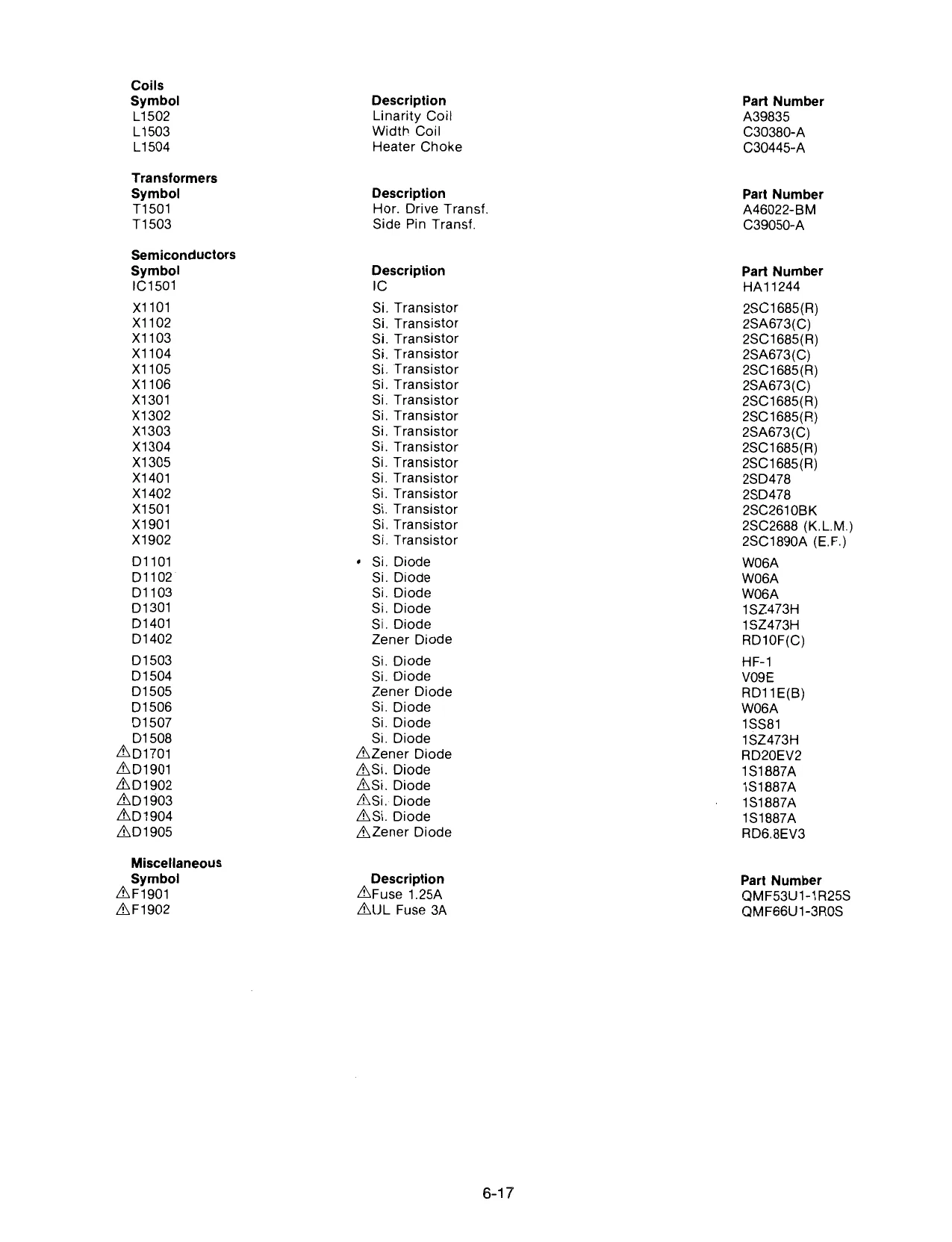
D911, D912
ct R921
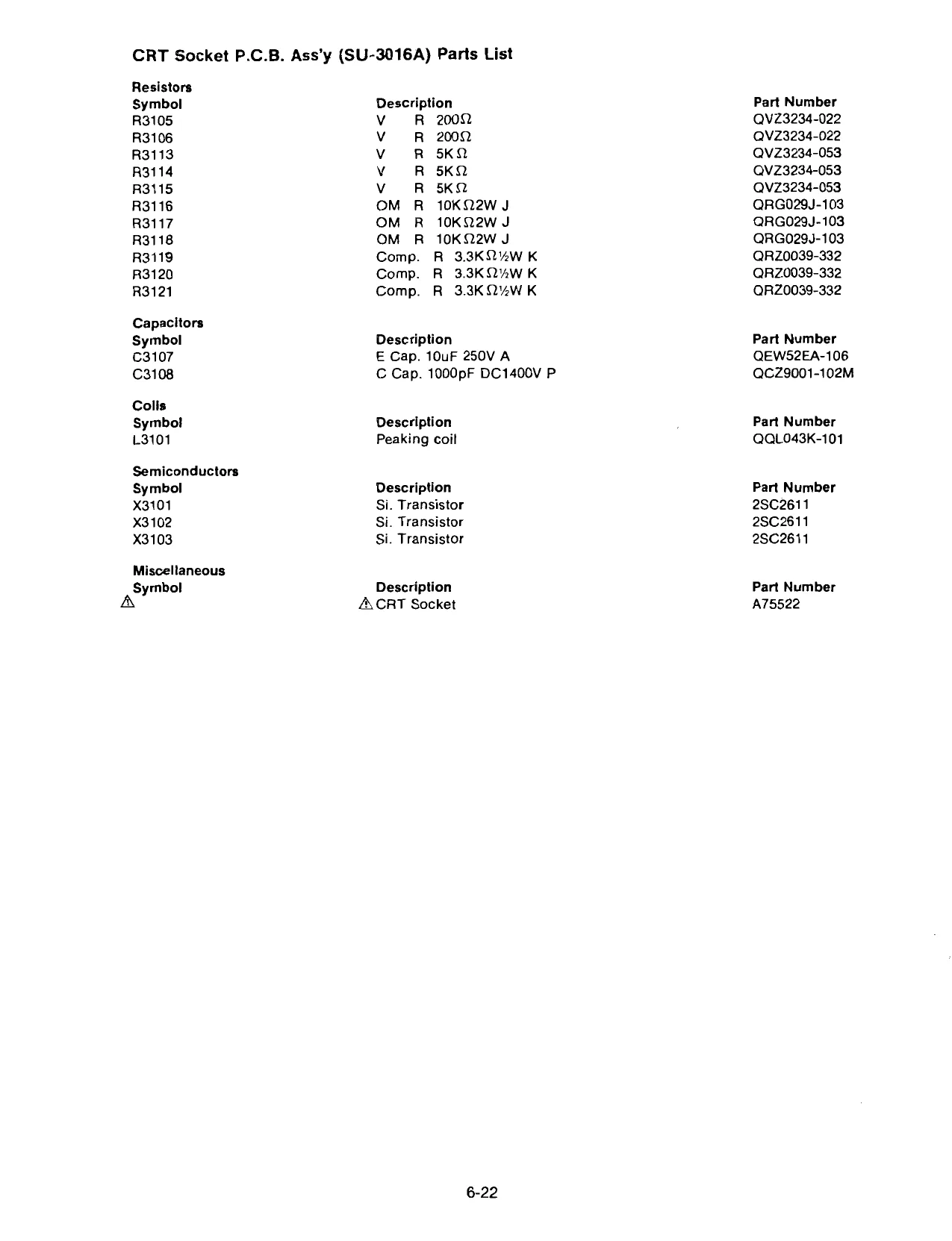
CRT Socket P.C.B. Ass’y (SU-
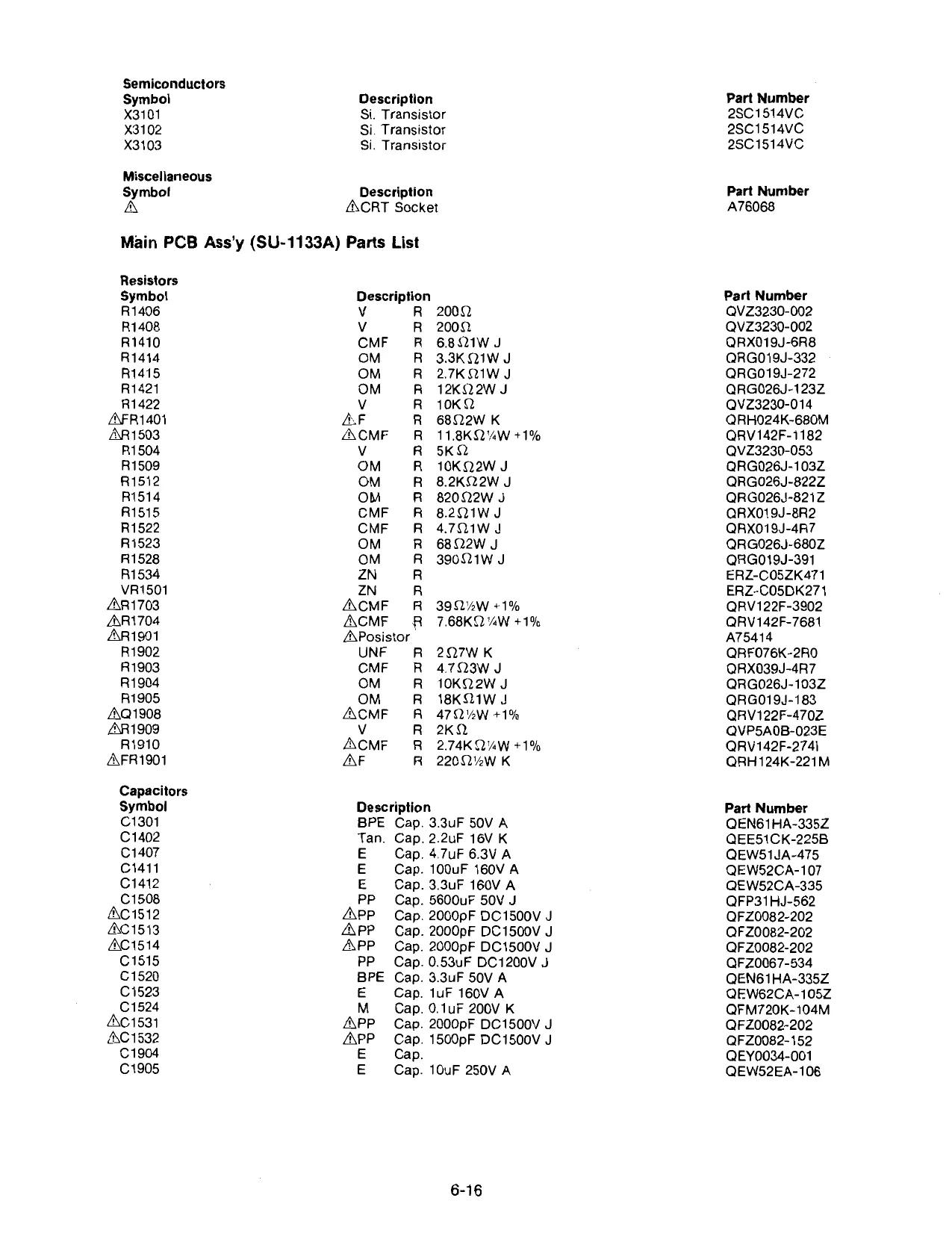
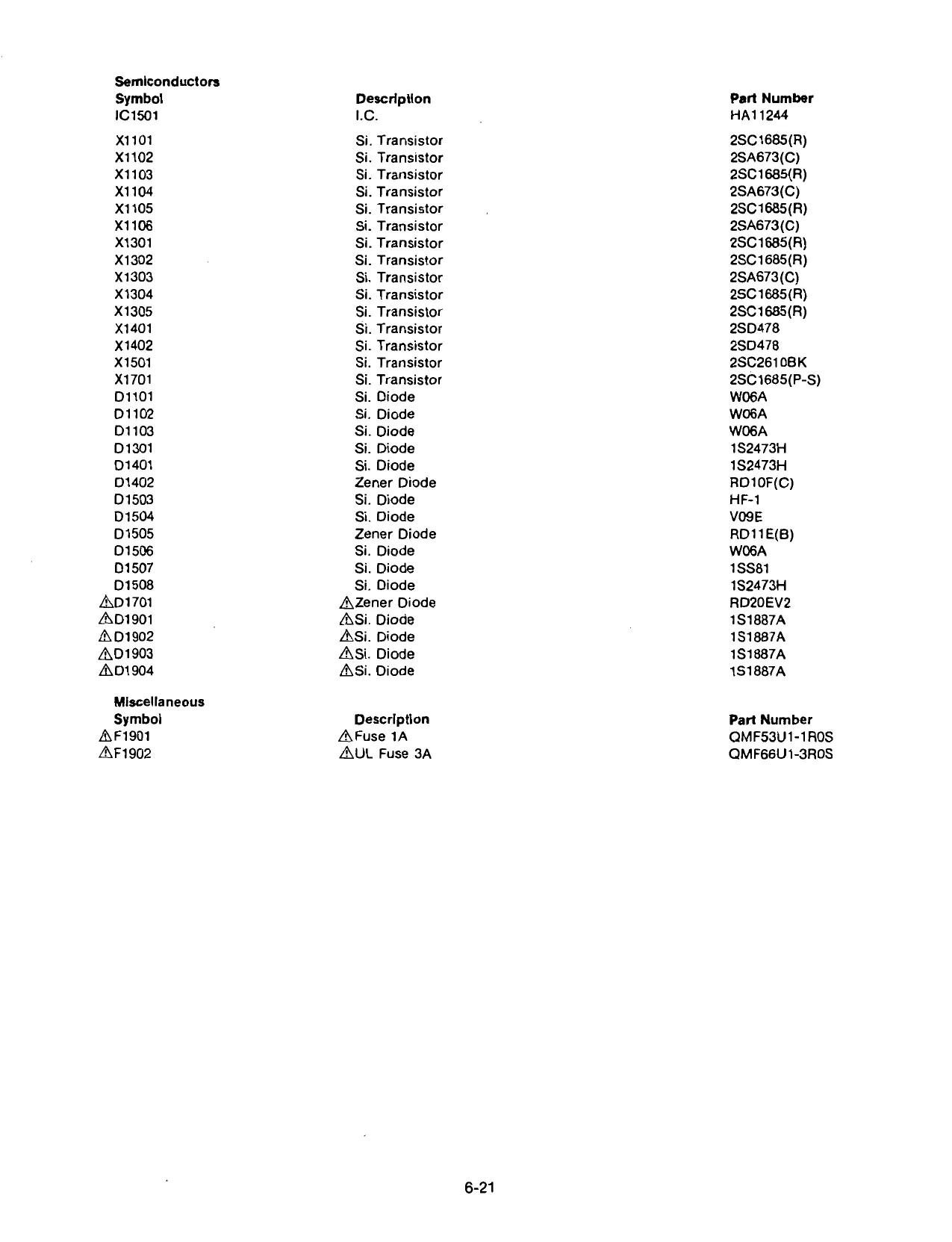
Resistors Symbol R3105 R3106 R3113 R3114 R3115 R3116 R3117 R3118 R3119 R3120 3121
Capacitors Symbol C3107 C3108
Coils Symbol L3101 Nut Retainer, Pix Tube Mtg. (4) Clip — P.C.B. Support Standoff Wire Terminal (Gnd. Strap) Terminal Lug (Gnd.) Groundstrap Assy. Grounding Spring Wire Hook (Gnd. Strap) Purity Shield Holddown Clamp Support Brkt. RH Support Brkt. LH Chassis Base Yoke Wedge (3)
Description Degaussing Coil Rectifier 1 Amp 600V (2) Pin Terminal (2) Pin Terminal Housing Purity Shield (2 pcs.) Purity Shield (2 pes.) Capacitor 100nF 10% 400V Resistor, Wirewound 332, 4W Fire Retardent Term. Strip 4 Lug
3032A) Parts List
Description Vv R 200 Vv R 200 Vv R 5K Vv R 5K v R 5K OM R 10KQ2W J OM R 10K Q2W J OM R 10KQ2W J Comp. R 3.3KQ%W K Comp. R 3.3KQ2“4W K Comp. R 3.3KQ%WK
Description E Cap. 10uF 250V A C Cap. 1000pF DC1400Vv P
Description Peaking Coil Part Number 17-7198-03 A29779-D = 21-141-01 A75034-B = 29-32-01 A29951-B A46600-A QRF258K-221 QCZ0101-005 2SD870 2SC1106A 31-610818-06 31-601418-12 33-255-01 33-494-01 33-629-02 33-670-010R-02 34-228-03 34-33-04 34-574-02 36-212-03 35-3053-02 35-2348-01 35-3890-01 35-3890-02 38-449-02 39-1233-01
Part Number 21-1007-30 28-22-27 34-708-01 34-709-01 35-3847-01 35-3847-02 48-171544-62 42-113301-03 34-492-09
Part. Number QVZ3234-022 QVZ3234-022 QVZ3234-053 QVZ3234-053 QVZ3234-053 QRGO029J-103 QRG029J-103 QRG029J-103 QRZ0039-332 QRZ0039-332 QRZ0039-332
Part Number QEWS53EA-106 QCZ9001-102M
Part Number QQL043K-101
This page is a drawing, shown as the original scan.
This page is a drawing, shown as the original scan.
This page is a drawing, shown as the original scan.
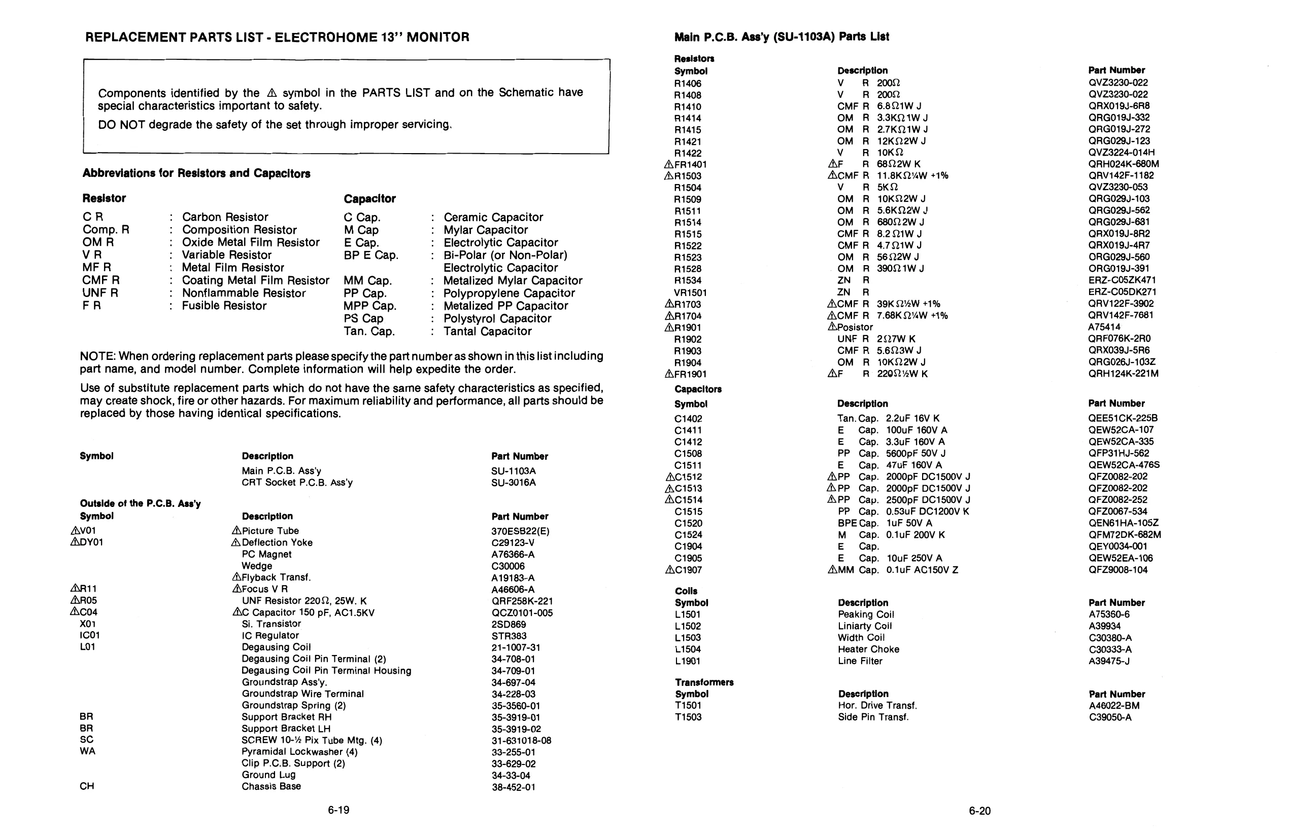
REPLACEMENT PARTS LIST - ELECTROHOME 13”’ MONITOR
Components identified by the A\ symbol in the PARTS LIST and on the Schematic have special characteristics important to safety.
DO NOT degrade the safety of the set through improper servicing.
Abbreviations for Resistors and Capacitors
Resistor Capacitor
| CR | : | Carbon Resistor | C Cap. |
| Comp. R | : | Composition Resistor | M Cap |
| OMR | : | Oxide Metal Film Resistor | E Cap. |
| VR | : | Variable Resistor | BP E Cap. |
| MFR | : | Metal Film Resistor | |
| CMF R | : | Coating Metal Film Resistor | MM Cap. |
| UNF R | : | Nonflammable Resistor | PP Cap. |
| FR | : | Fusible Resistor | MPP Cap. |
PS Cap Tan. Cap. Ceramic Capacitor Mylar Capacitor Electrolytic Capacitor Bi-Polar (or Non-Polar) Electrolytic Capacitor Metalized Mylar Capacitor Polypropylene Capacitor Metalized PP Capacitor Polystyrol Capacitor Tantal Capacitor
Use of substitute replacement parts which do not have the same safety characteristics as specified, may create shock, fire or other hazards. For maximum reliability and performance, all parts should be replaced by those having identical specifications.
Symbol
Outside of the P.C.B. Ass’y Symbol Asvo1 ADY01
AR11 ASROS; Aco4 X01 1c01 Lo1
BR BR sc WA
CH Description Main P.C.B. Ass'y CRT Socket P.C.B. Ass'y
Description A’Picture Tube A\Deflection Yoke PC Magnet Wedge AFlyback Transf. Focus V R UNF Resistor 2202, 25W. K AC Capacitor 150 pF, AC1.5KV Si. Transistor IC Regulator Degausing Coil Degausing Coil Pin Terminal (2) Degausing Coil Pin Terminal Housing Groundstrap Assy. Groundstrap Wire Terminal Groundstrap Spring (2) Support Bracket RH Support Bracket LH SCREW 10-% Pix Tube Mtg. (4) Pyramidal Lockwasher (4) Clip P.C.B. Support (2) Ground Lug Chassis Base
6-19 Part Number
SU-1103A SU-3016A
Part Number
370ES822(E) 29123-V A76366-A 30006 A19183-A A46606-A QRF258K-221 QCZ0101-005 2SD869 STR383 21-1007-31 34-708-01 34-709-01 34-697-04 34-228-03 35-3560-01 35-3919-01 35-3919-02 31-631018-08 33-255-01 33-629-02 34-33-04 38-452-01 Main P.C.B. Ass'y (SU-1103A) Parts List
Resistors Symbol R1406 R1408 R1410 R1414 R1415 R1421 R1422 ASFR1401 AXR1503 R1504 R1509 R1511 R1514 R1515 R1522 R1523 R1528 R1534 VR1501 AsR1703 ASR1704 AX\R1901 R1902 R1903 R1904 AFR1901
Capacitors Symbol ©1402 c1411 C1412 C1508 C1511 AC1512 AC1513 AC1514 C1515 C1520 1524 1904 1905 A\C1907
Coils Symbol L1501 L1502 L1503 11504 L1901
Transformers Symbol 71501 T1503 Descripti voeR vVoR CMF R OM R OM R OM R VoR AF OR ASCMF R voR OM R OM R OM R CMF R CMF R OM R OM R ZN R ZN R A\CMF R ACMF R APosistor UNF R CMF R OM R AF OR
Descripti. Tan. Cap. E Cap. E Cap. PP Cap. E Cap. AXPP Cap. AXPP Cap. AXPP Cap. PP Cap. BPE Cap. M_ Cap. ion 2002 2002 6.8Q1W J 3.3KQ1W J 2.7KQ1W J 12KN2W J 10KQ. 6822W K 11.8KQUW +1% 5KQ. 10K22W J 5.6KQ2W J 6802 2W J 8.201W J 4.7Q1W J 56Q2W J 3902.1W J
39K DAW +1% 7.68K QYUW 1%
2Q7W K 5.623W J 1OKQ2W J 2202%W K
jon
2.2uF 16V K 100uF 160V A 3.3uF 160V A 5600pF 50V J ATuF 160V A 2000pF DC1500V J 2000pF DC1500V J 2500pF DC1500V J 0.53uF DC1200V K 1uF 50V A 0.1uF 200V K E Cap. E Cap. A\MM Cap. 10uF 250V A 0.1uF AC150V Z
Description Peaking Coil Liniarty Coil Width Coil Heater Choke Line Filter
Description Hor. Drive Transf. Side Pin Transf.
6-20 Part Number QVZ3230-022 QVZ3230-022 QRX019J-6R8 QRGO019J-332 QRG019J-272 QRG029J-123 QVZ3224-014H QRH024K-680M QRV142F-1182 QVZ3230-053 QRGO029J-103 QRG029J-562 QRG029J-631 QRX019J-8R2 QRX019J-4R7 ORG029J-560 ORG019J-391 ERZ-C05ZK471 ERZ-C05DK271 QRV122F-3902 QRV142F-7681 A75414 QRFO76K-2RO QRX039J-5R6 QRGO026J-103Z QRH124K-221M
Part Number
QEES1CK-225B QEW52CA-107 QEW52CA-335 QFP31HJ-562 QEWS2CA-476S QFZ0082-202 QFZ0082-202 QFZ0082-252 QFZ0067-534 QEN61HA-105Z QFM72DK-682M QEY0034-001 QEWS2EA-106 QFZ9008-104
Part Number A75360-6 A39934 30380-A C30333-A A39475-J
Part Number A46022-BM C39050-A
This page is a drawing, shown as the original scan.
This page is a drawing, shown as the original scan.
VII. Coin Door Maintenance
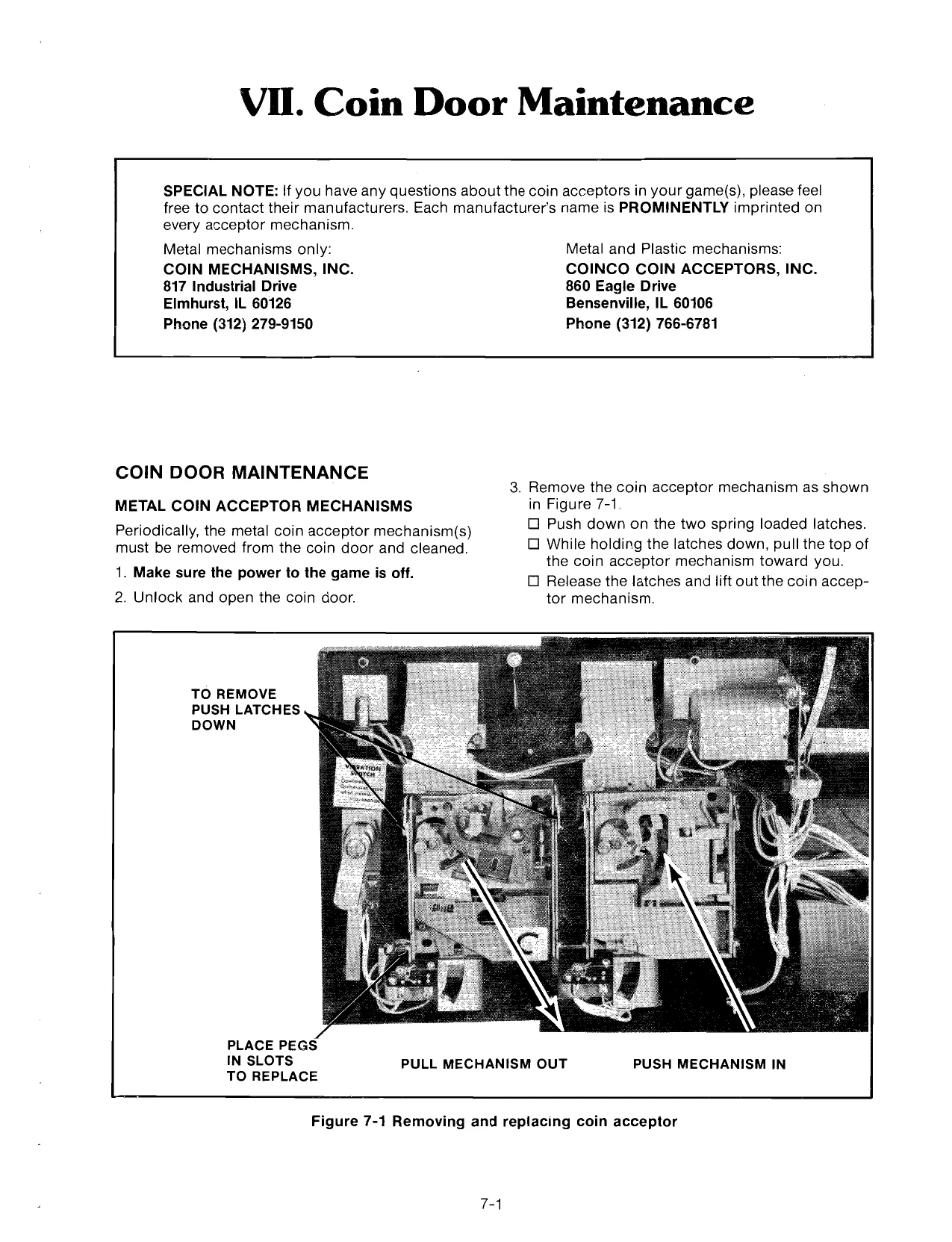
SPECIAL NOTE: If you have any questions about the coin acceptors in your game(s), please feel free to contact their manufacturers. Each manufacturer's name is PROMINENTLY imprinted on every acceptor mechanism. Metal mechanisms only: COIN MECHANISMS, INC. 817 Industrial Drive Elmhurst, iL 60126 Phone (312) 279-9150
COIN DOOR MAINTENANCE
METAL COIN ACCEPTOR MECHANISMS
Periodically, the metal coin acceptor mechanism(s) must be removed from the coin door and cleaned.
- Make sure the power to the game is off.
- Unlock and open the coin door.
TO REMOVE PUSH LATCHES DOWN
PLACE PEGS IN SLOTS TO REPLACE PULL MECHANISM OUT Metal and Plastic mechanisms: COINCO COIN ACCEPTORS, INC. 860 Eagle Drive Bensenville, IL 60106 Phone (312) 766-6781
- Remove the coin acceptor mechanism as shown in Figure 7-1 O Push down on the two spring loaded latches. O While holding the latches down, pull the top of the coin acceptor mechanism toward you. O Release the latches and lift out the coin acceptor mechanism.
PUSH MECHANISM IN
Figure 7-1 Removing and replacing coin acceptor
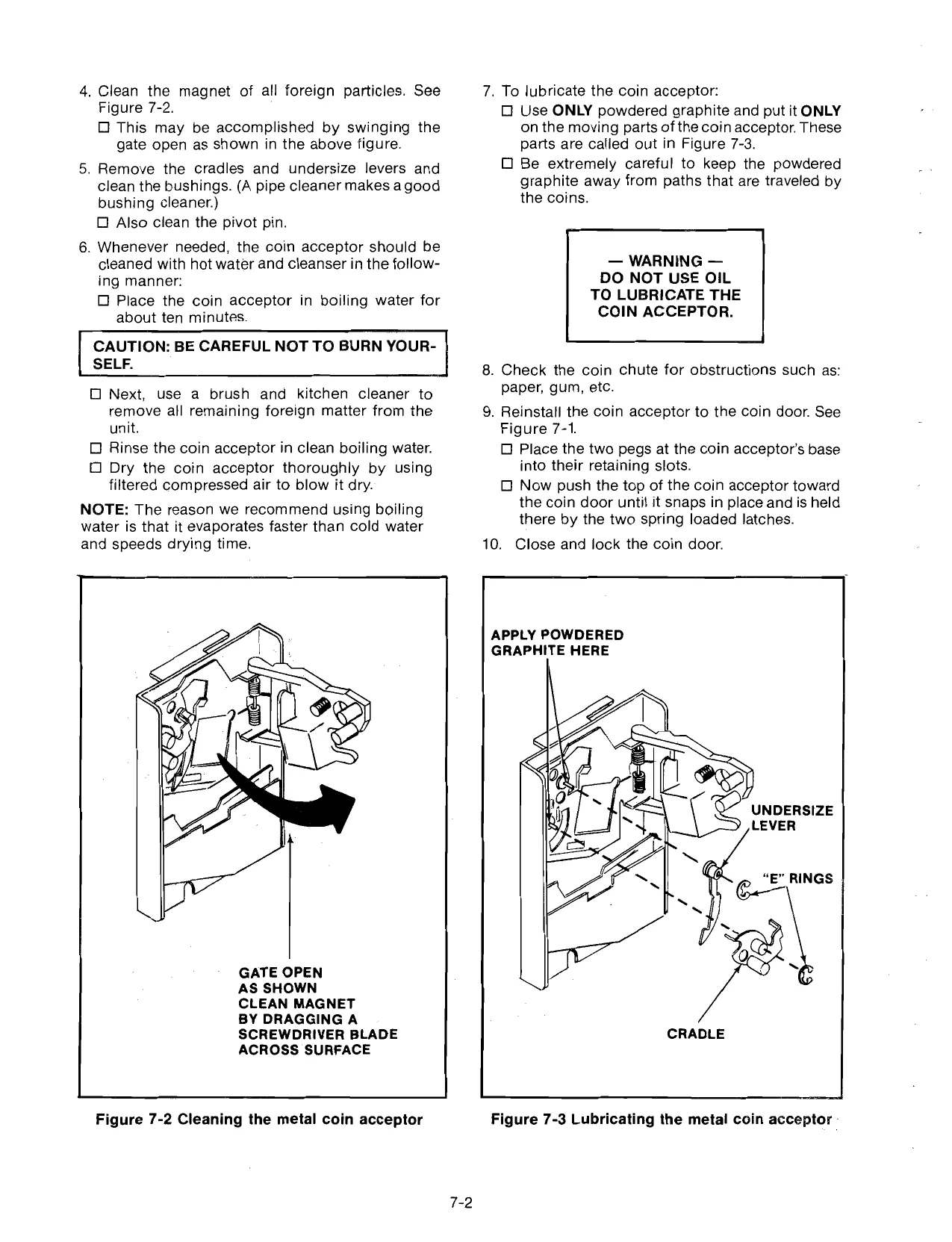
4, Clean the magnet of all foreign particles. See Figure 7-2. O This may be accomplished by swinging the gate open as shown in the above figure.
- Remove the cradles and undersize levers and clean the bushings. (A pipe cleaner makes agood bushing cleaner.) O Also clean the pivot pin.
- Whenever needed, the coin acceptor should be cleaned with hot water and cleanser in the following manner: O Place the coin acceptor in boiling water for about ten minutes.
O Next, use a brush and kitchen cleaner to remove all remaining foreign matter from the unit. D Rinse the coin acceptor in clean boiling water. C Dry the coin acceptor thoroughly by using filtered compressed air to blow it dry.
GATE OPEN AS SHOWN CLEAN MAGNET BY DRAGGING A SCREWDRIVER BLADE ACROSS SURFACE
Figure 7-2 Cleaning the metal coin acceptor
- To lubricate the coin acceptor: 0 Use ONLY powdered graphite and put it ONLY on the moving parts of the coin acceptor. These parts are called out in Figure 7-3. O Be extremely careful to keep the powdered graphite away from paths that are traveled by the coins.
- WARNING — DO NOT USE OIL TO LUBRICATE THE COIN ACCEPTOR.
- Check the coin chute for obstructions such as: paper, gum, etc.
- Reinstall the coin acceptor to the coin door. See Figure 7-1. O Place the two pegs at the coin acceptor’s base into their retaining slots. O Now push the top of the coin acceptor toward the coin door unti! it snaps in place and is held there by the two spring loaded latches.
- Close and lock the coin door.
APPLY POWDERED GRAPHITE HERE
CRADLE
Figure 7-3 Lubricating the metal coin acceptor
7-2
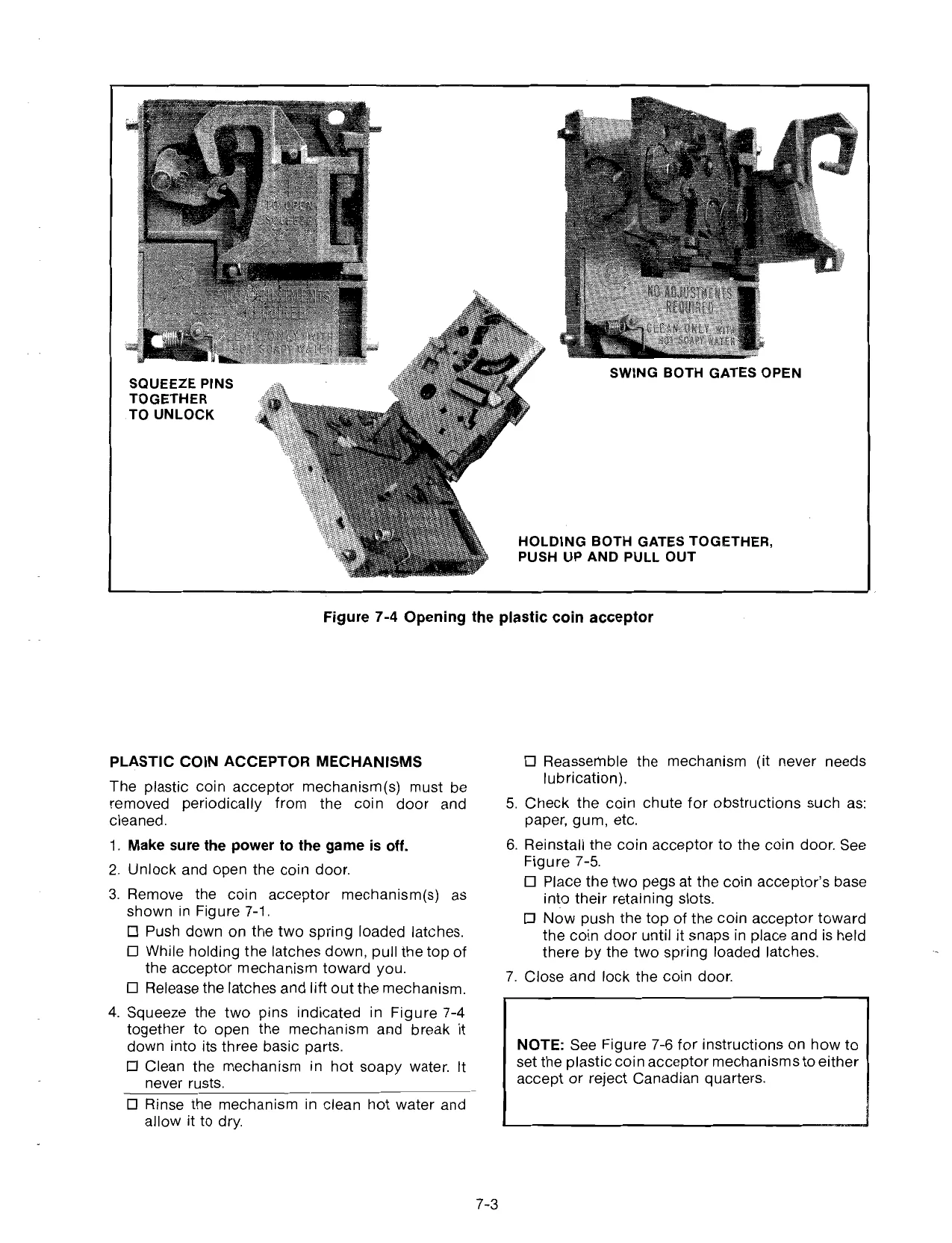
SQUEEZE PINS TOGETHER TO UNLOCK
HOLDING BOTH GATES TOGETHER, PUSH UP AND PULL OUT
Figure 7-4 Opening the plastic coin acceptor
PLASTIC COIN ACCEPTOR MECHANISMS The plastic coin acceptor mechanism(s) must be removed periodically from the coin door and cleaned.
- Make sure the power to the game is off.
- Unlock and open the coin door.
- Remove the coin acceptor mechanism(s) as shown in Figure 7-1. O Push down on the two spring loaded latches. D While holding the latches down, pull the top of the acceptor mechanism toward you. O Release the latches and lift out the mechanism.
- Squeeze the two pins indicated in Figure 7-4 together to open the mechanism and break it down into its three basic parts. O Clean the mechanism in hot soapy water. It never rusts. 0 Rinse the mechanism in clean hot water and allow it to dry. UO Reassemble the mechanism (it never needs lubrication).
- Check the coin chute for obstructions such as: paper, gum, etc.
- Reinstall the coin acceptor to the coin door. See Figure 7-5. O Place the two pegs at the coin acceptor’s base into their retaining slots. D Now push the top of the coin acceptor toward the coin door until it snaps in place and is held there by the two spring loaded latches.
- Close and lock the coin door.
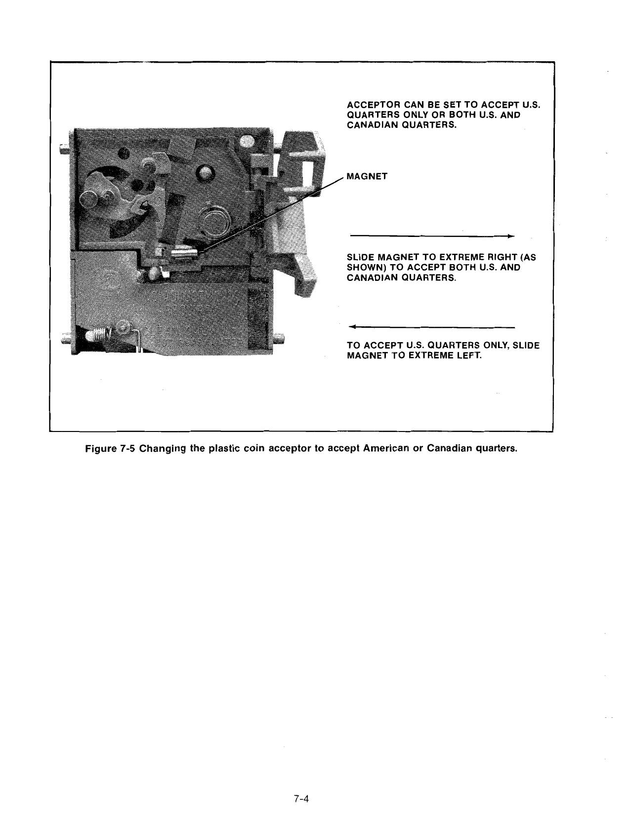
This page is a drawing, shown as the original scan.
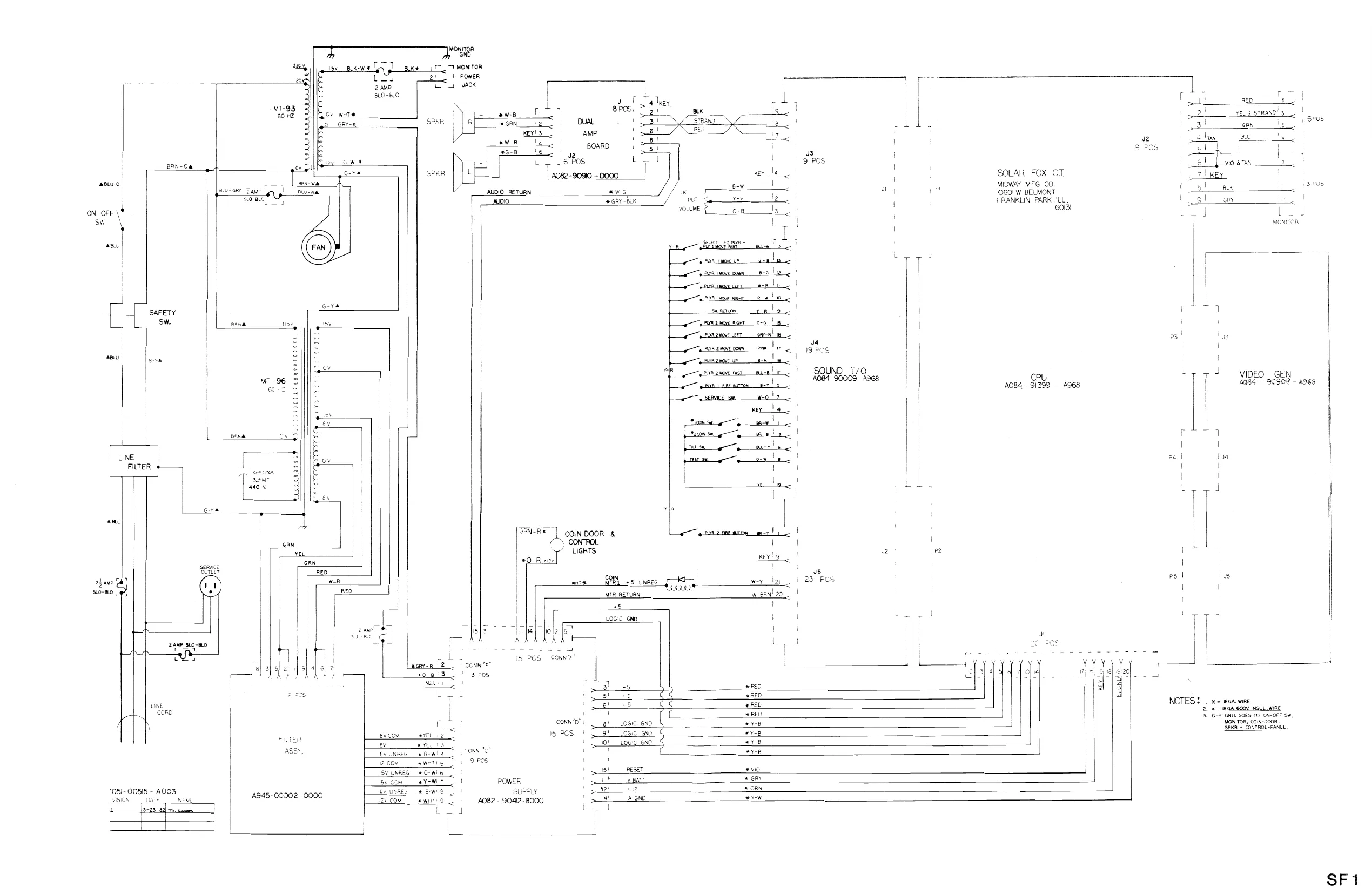
This page is a drawing, shown as the original scan.
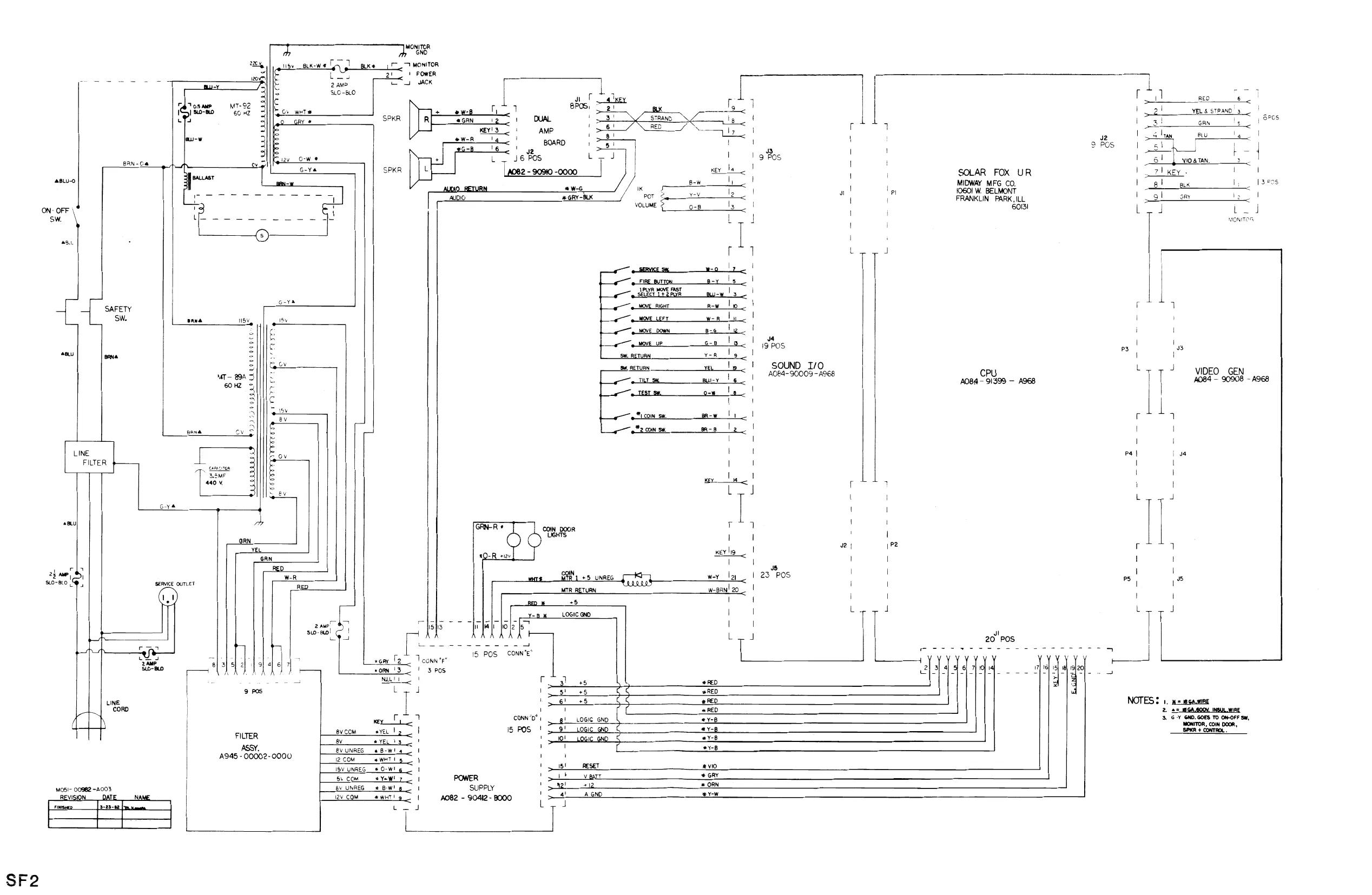
This page is a drawing, shown as the original scan.
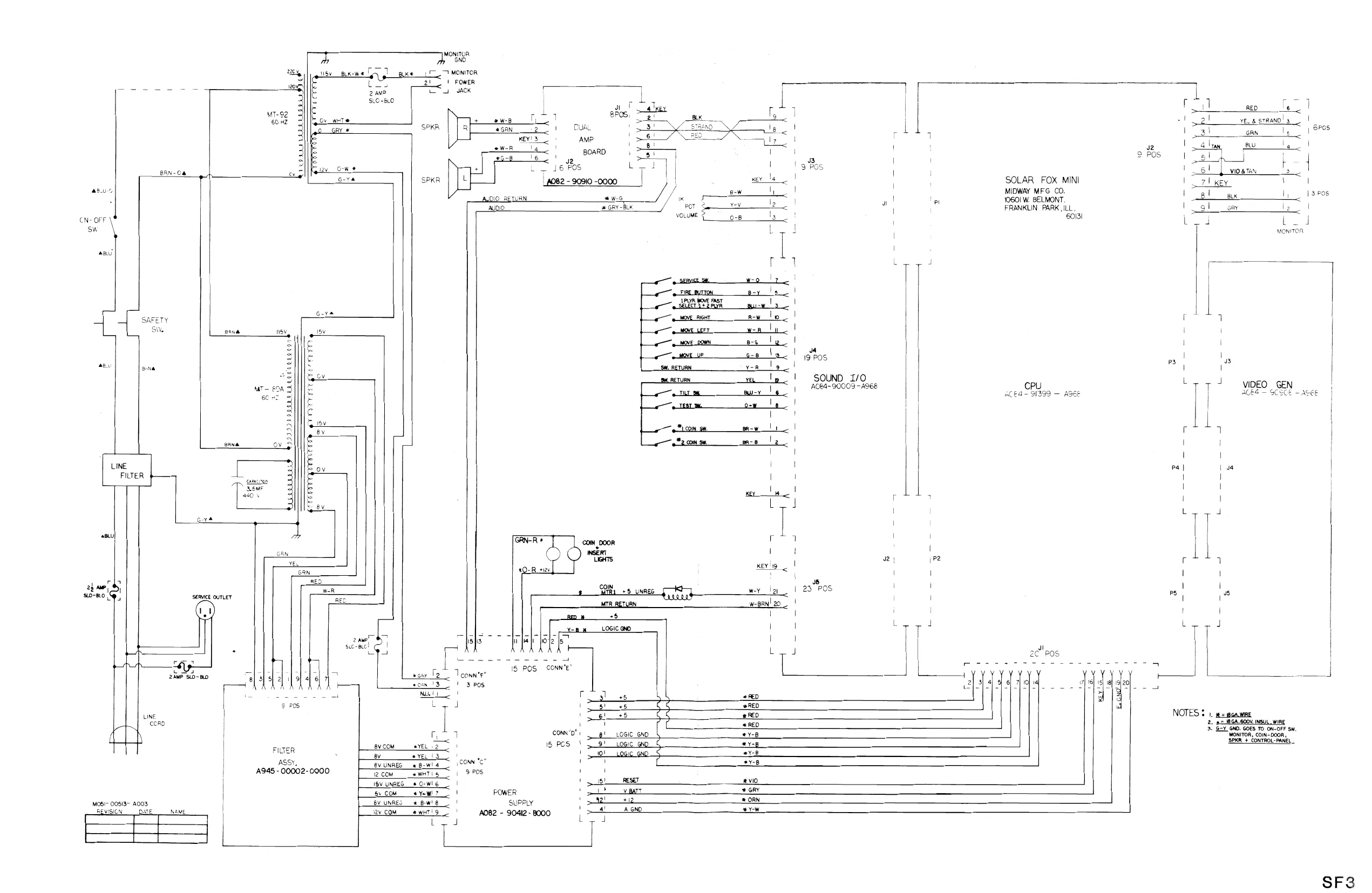
This page is a drawing, shown as the original scan.
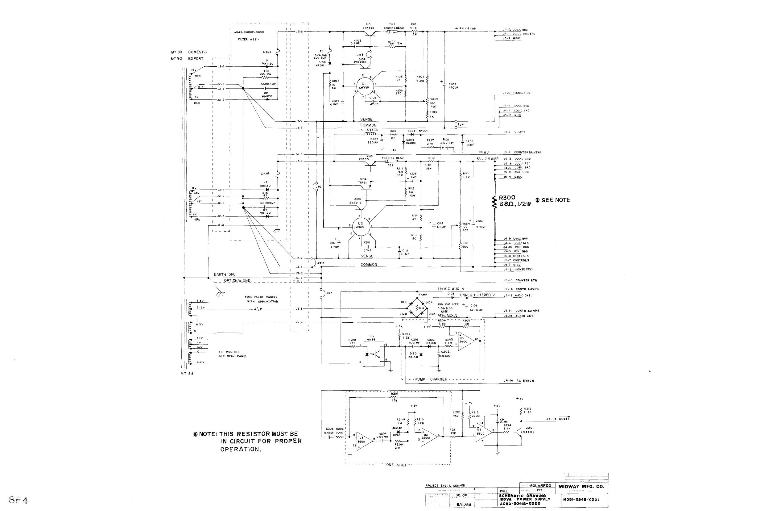
This page is a drawing, shown as the original scan.
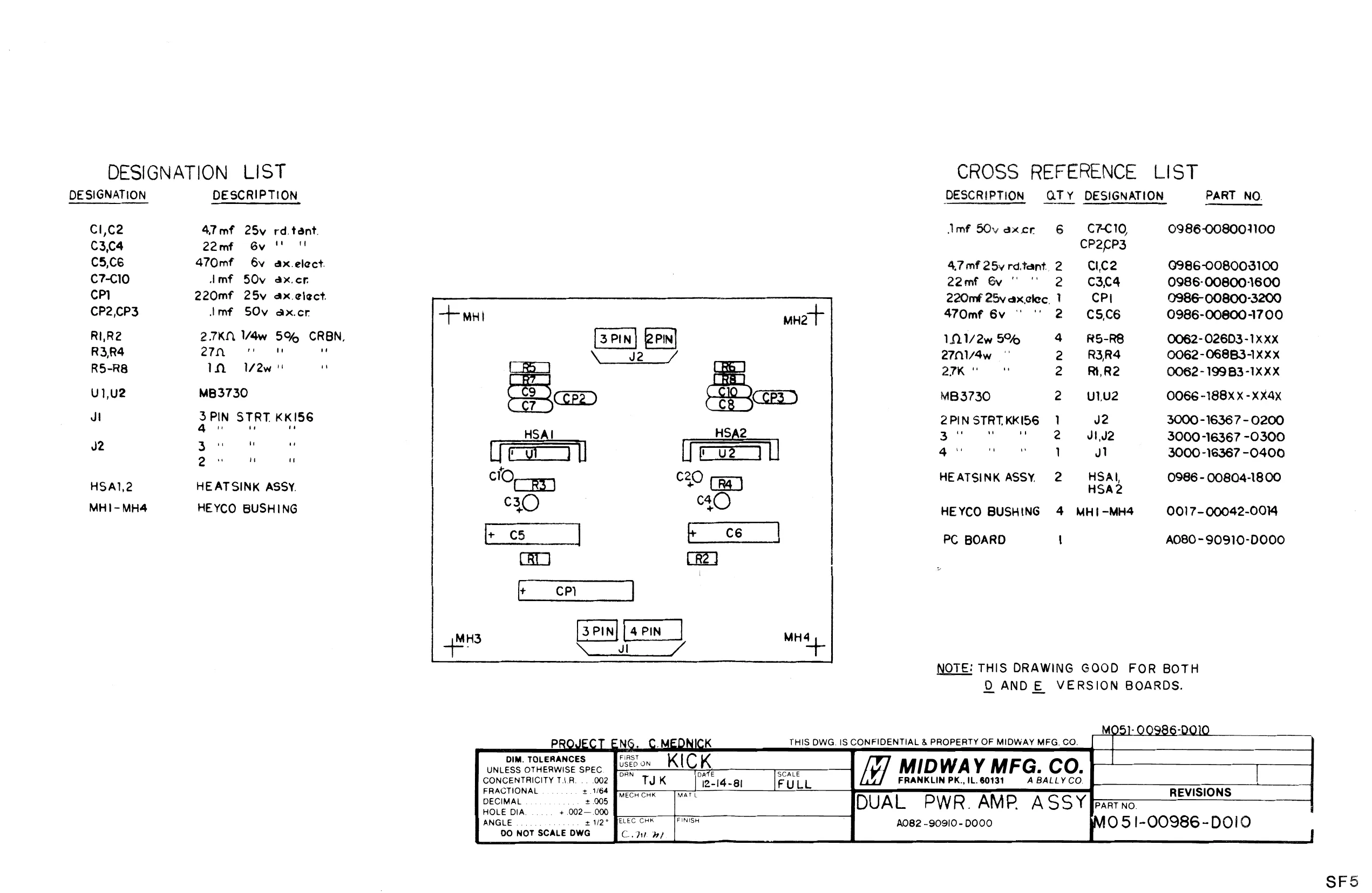
This page is a drawing, shown as the original scan.
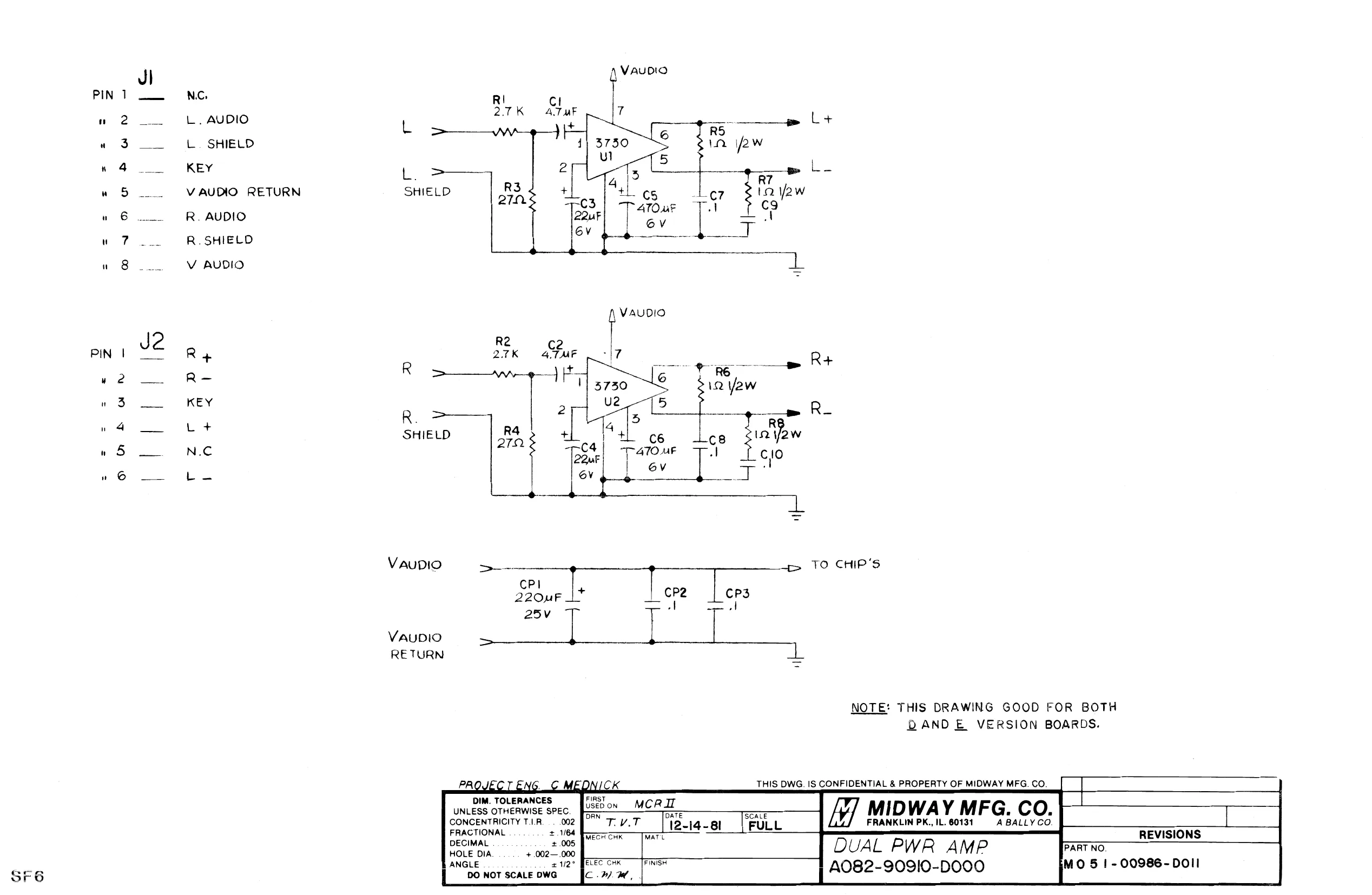
This page is a drawing, shown as the original scan.
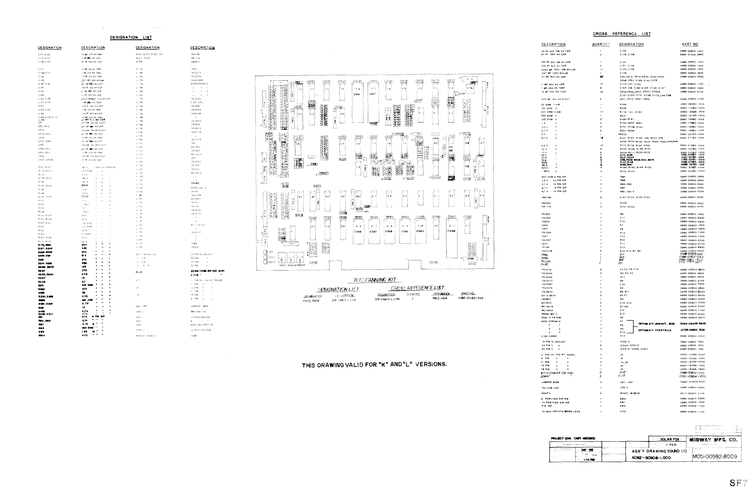
This page is a drawing, shown as the original scan.
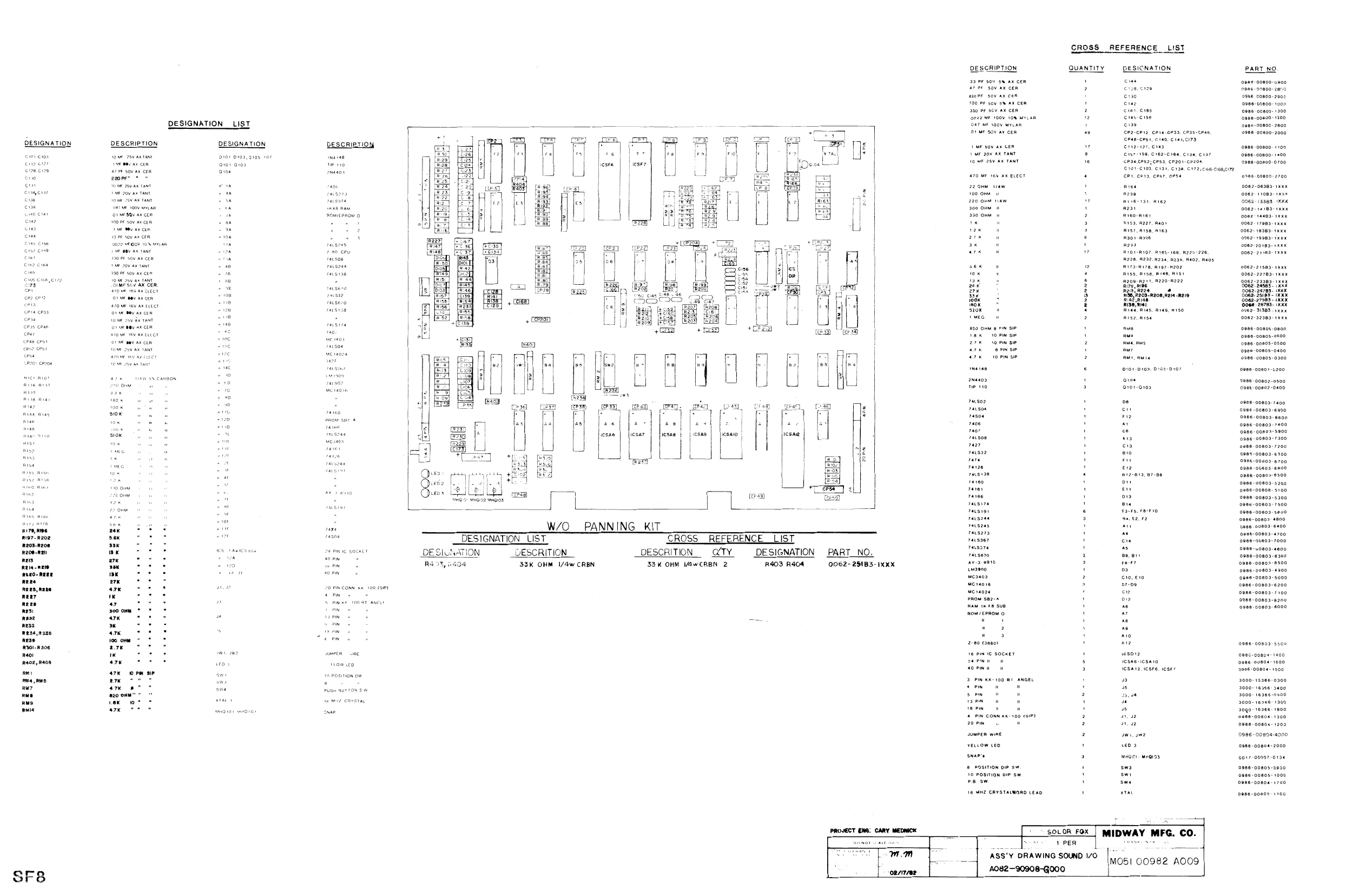
This page is a drawing, shown as the original scan.
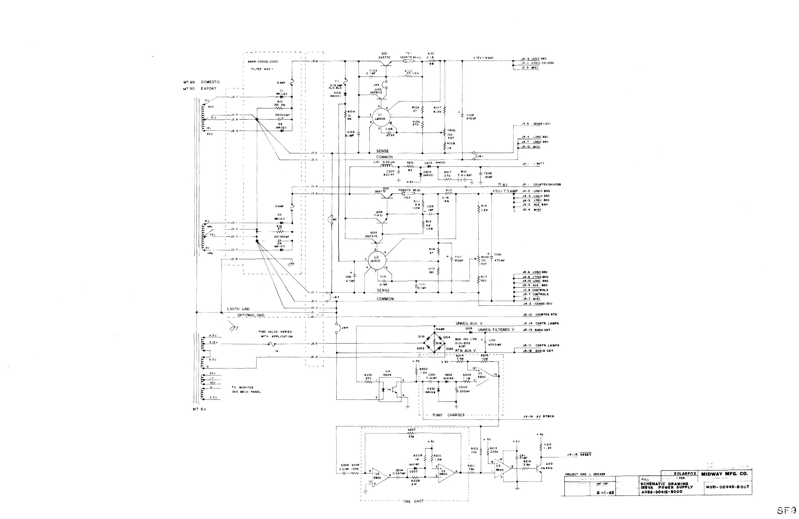
This page is a drawing, shown as the original scan.
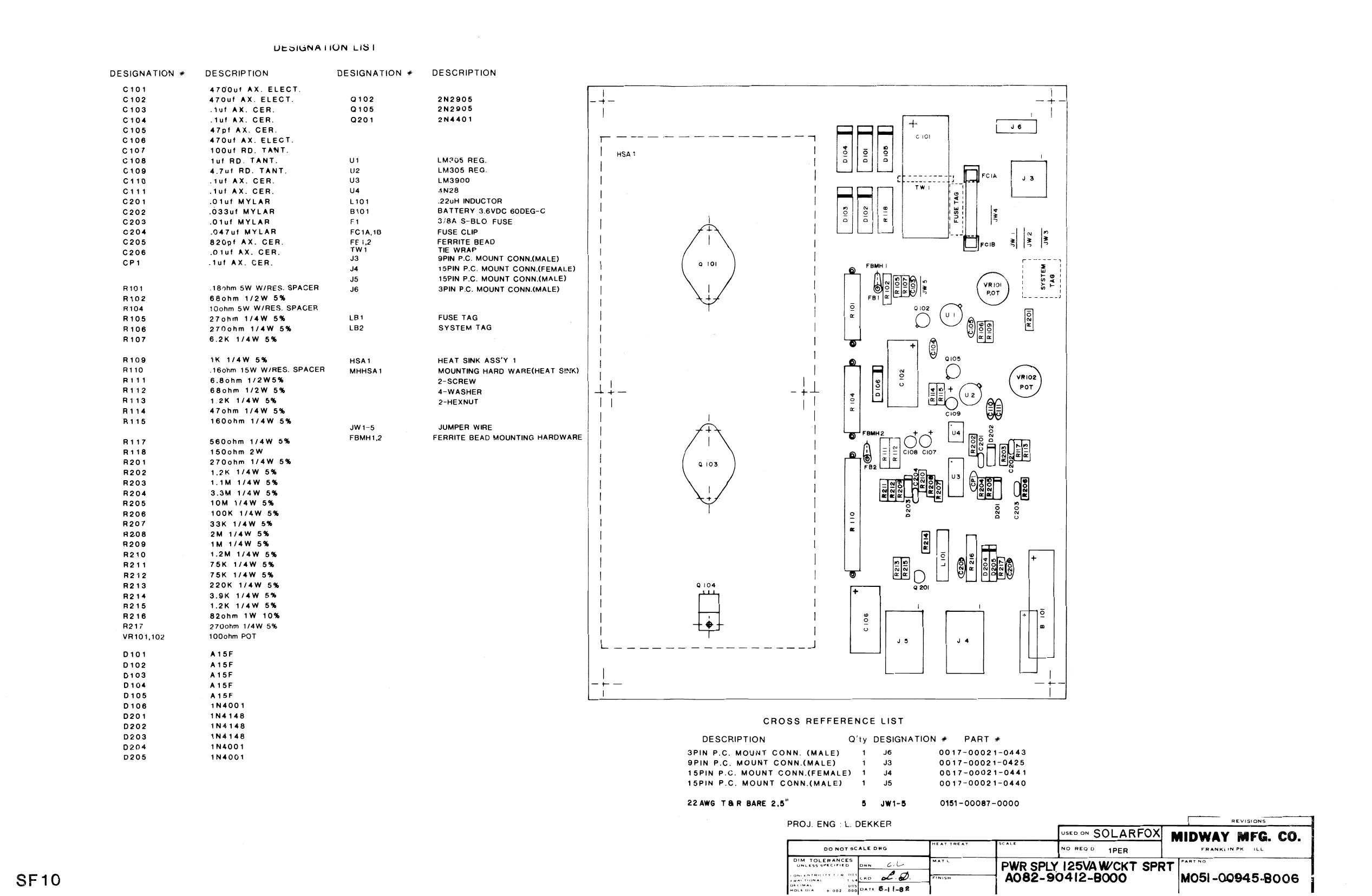
This page is a drawing, shown as the original scan.
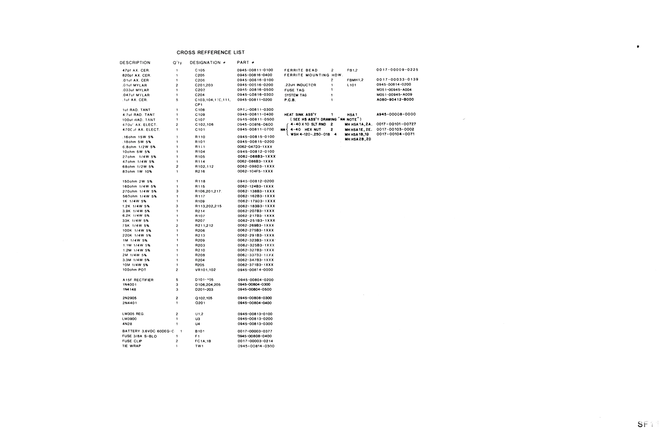
This page is a drawing, shown as the original scan.
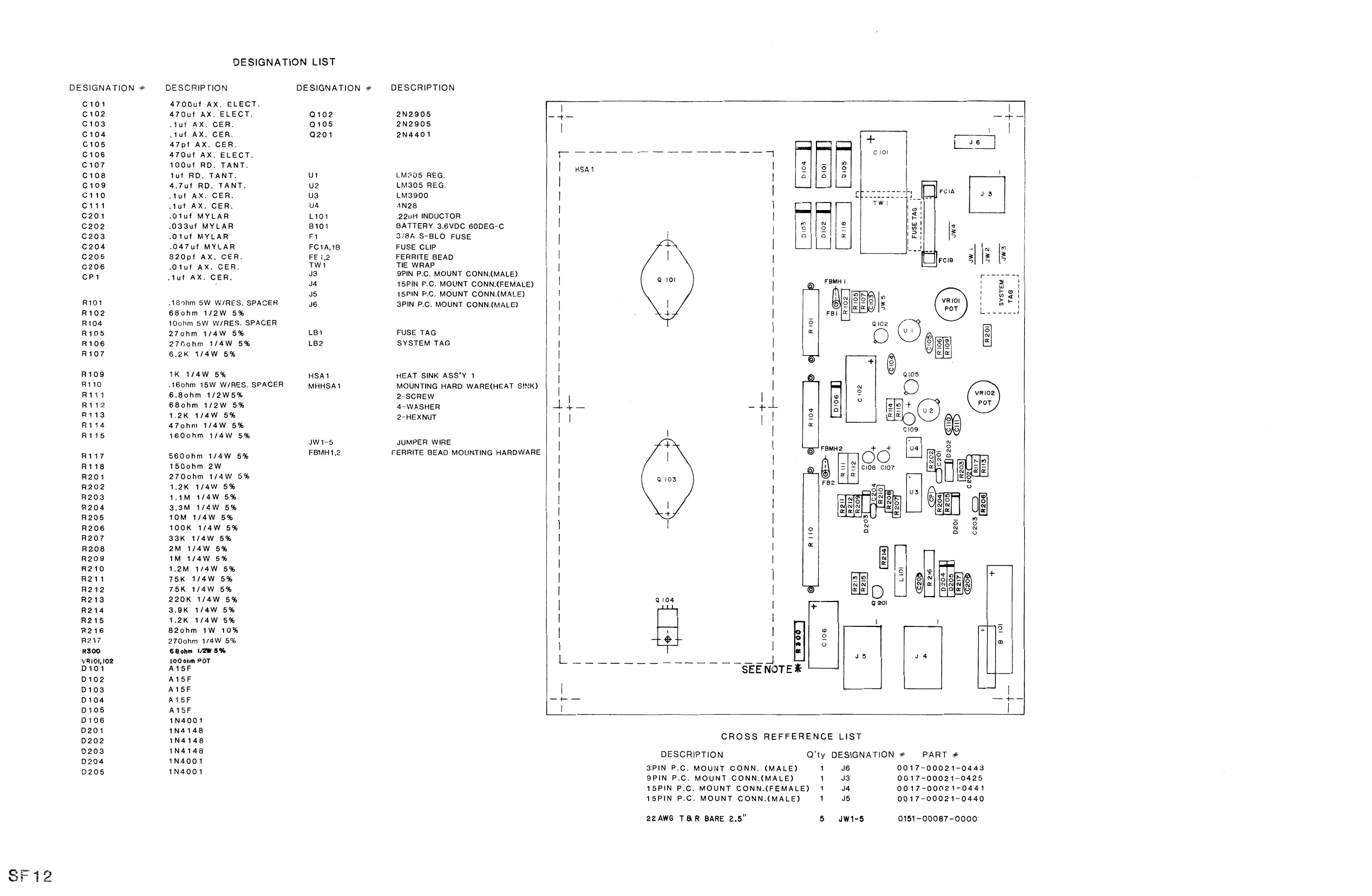
This page is a drawing, shown as the original scan.
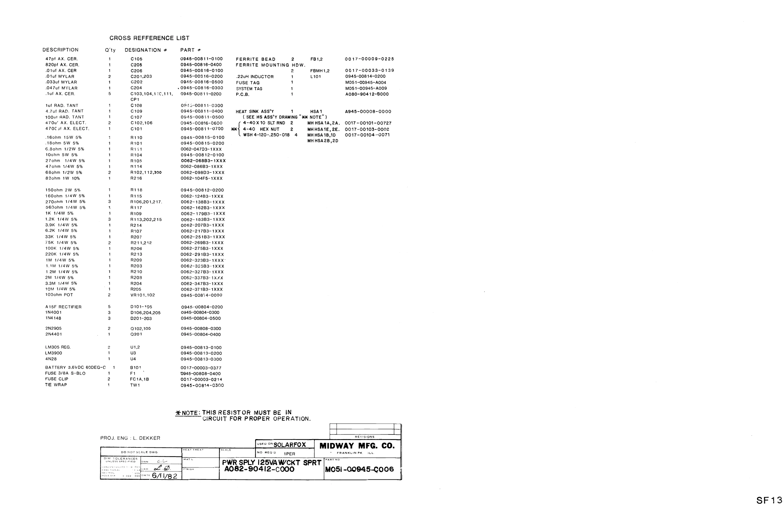
This page is a drawing, shown as the original scan.
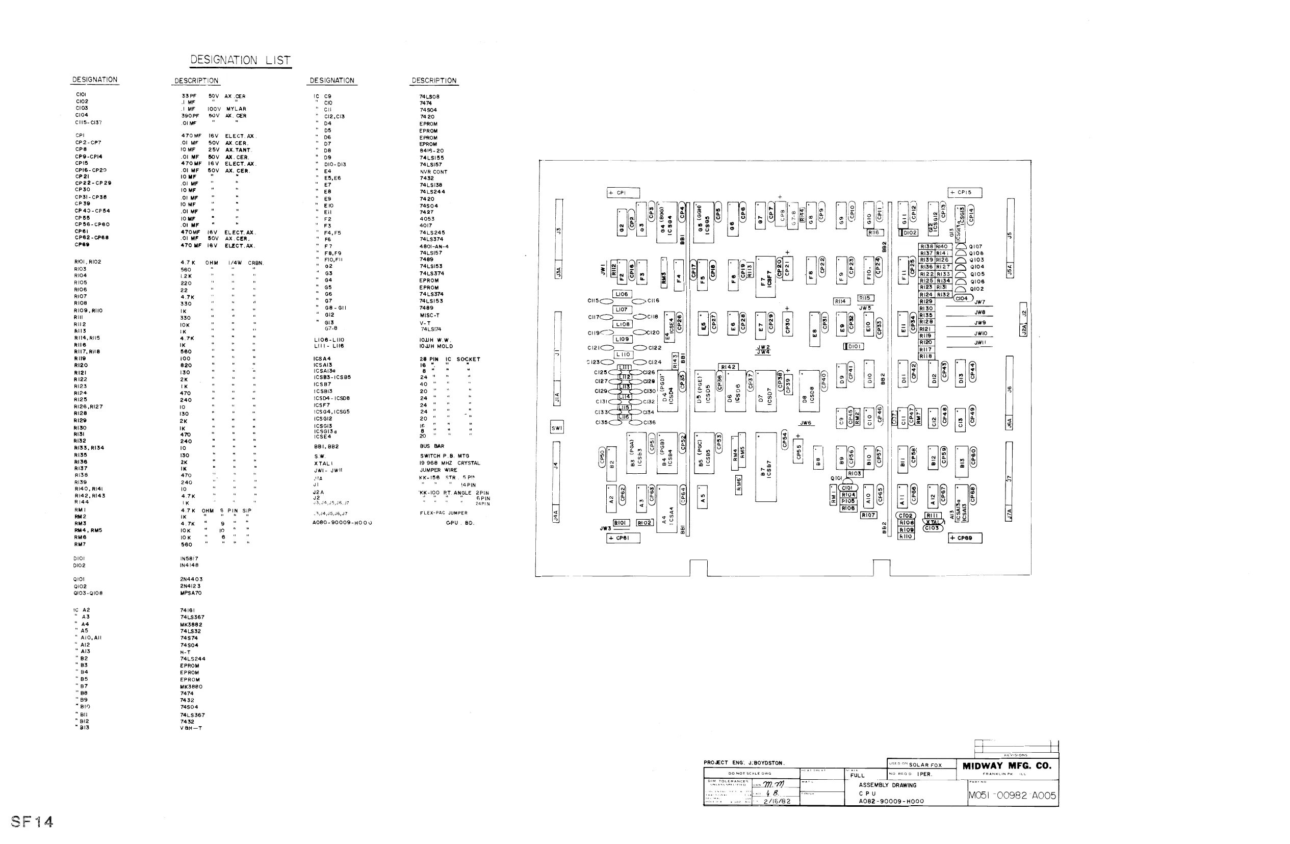
This page is a drawing, shown as the original scan.
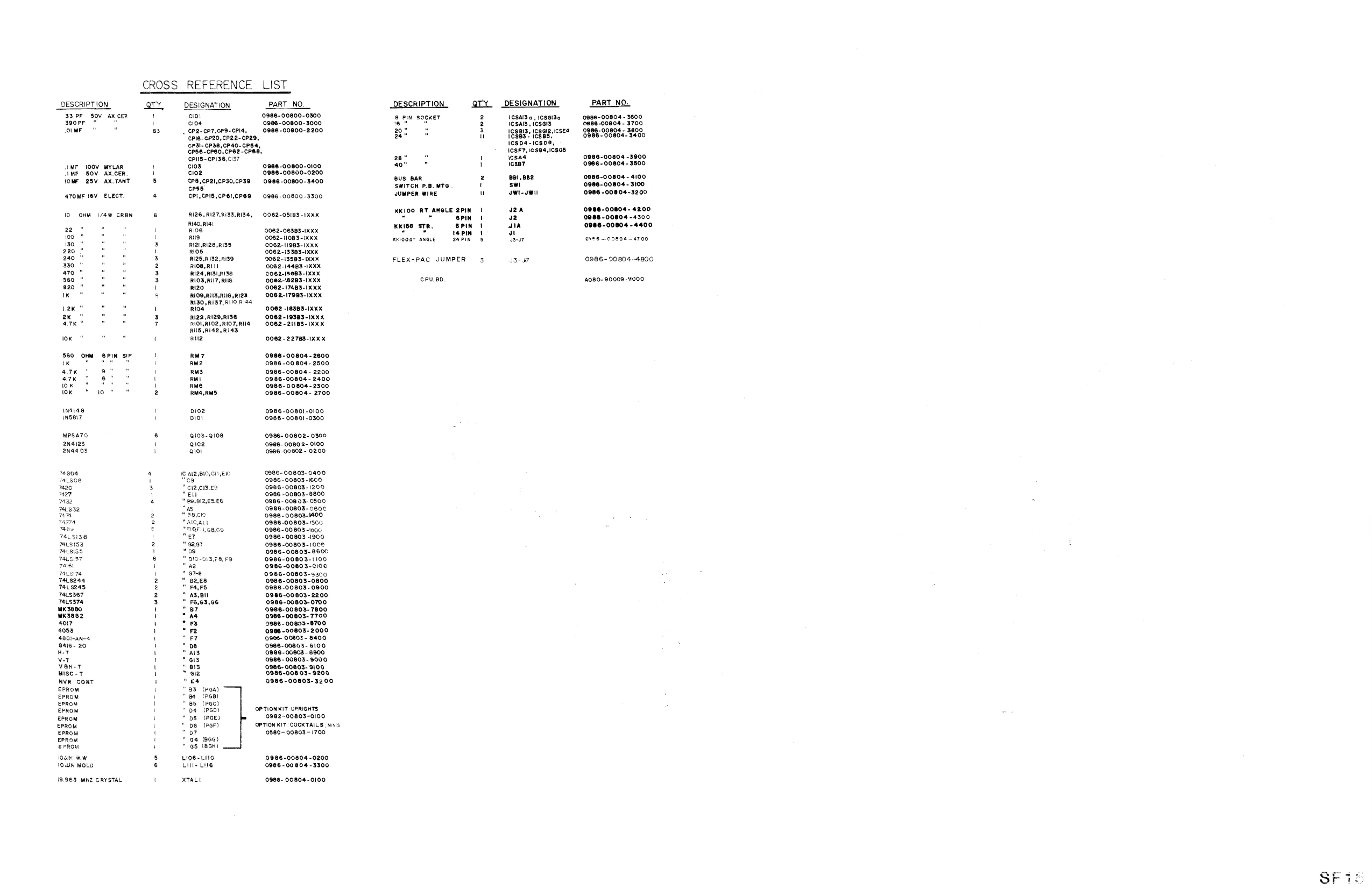
This page is a drawing, shown as the original scan.
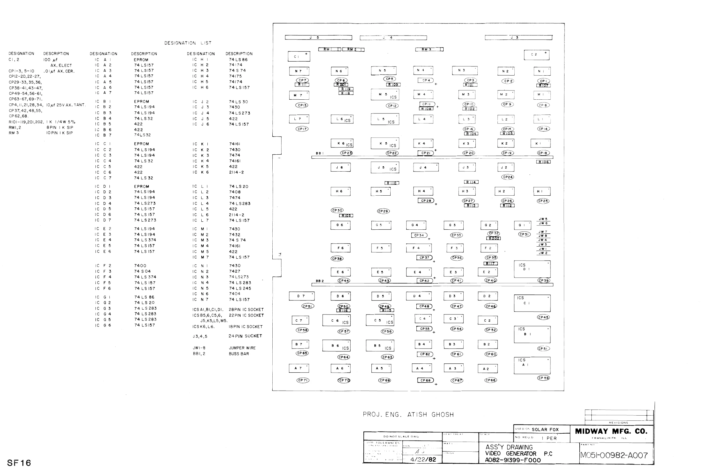
This page is a drawing, shown as the original scan.
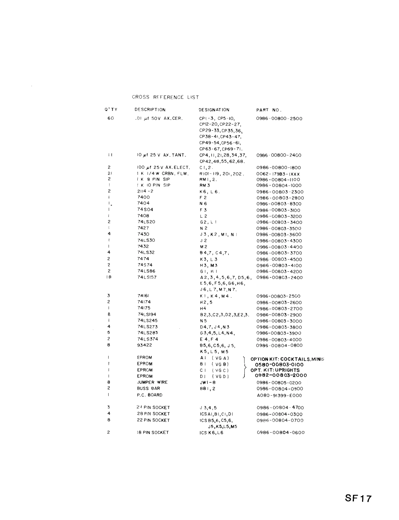
This page is a drawing, shown as the original scan.
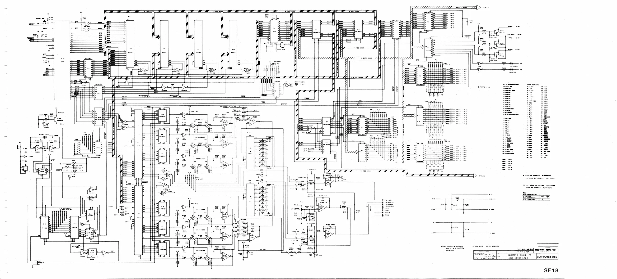
This page is a drawing, shown as the original scan.
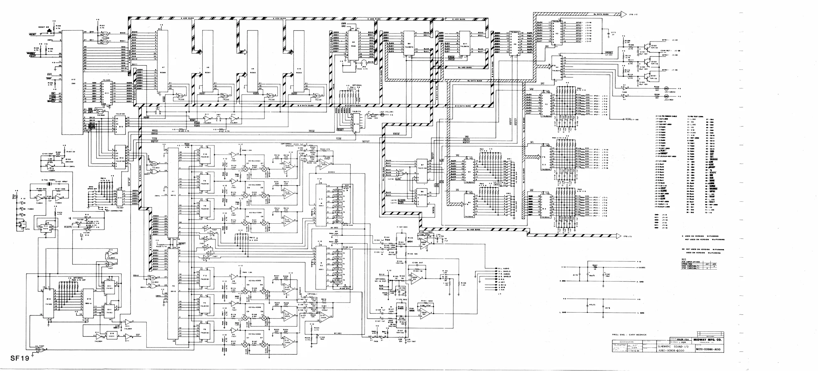
This page is a drawing, shown as the original scan.
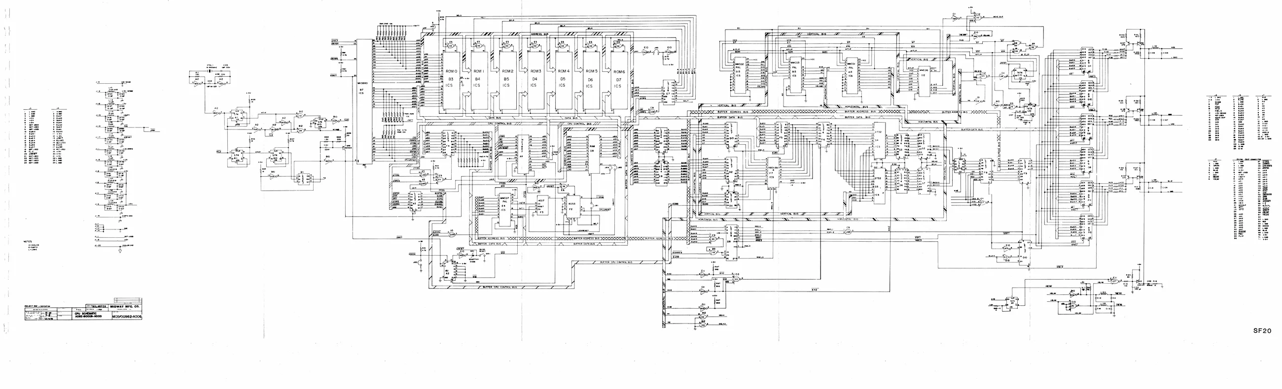
This page is a drawing, shown as the original scan.
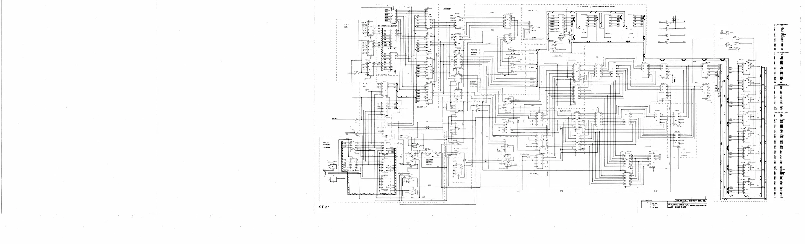
This page is a drawing, shown as the original scan.