Indy 4 TM-055
Indy 4 (Atari/Kee, 1976) · Technical Manual · 84 pages · 32 sections · original scan
TM-055
Operation - Maintenance + Service Manual
ATARI Innovative leisure
5s) 334690. Winchester Blvd. =< tags Gatos, CA-95030 J -Phyeine- 408/374-2440 owe Sex 357-488 Copyright @)1976 by Atari, Inc.
iM SNOUT “NBO RREgaO Sead receete Aou suoszed 03 pesoTosTp: FSR SU eee
- Fz . ee
- eee oe Soop ee 30 soueuequTeM « Jo
- ee pubes Sa x ee tae me = TOGNNCO NI SHEET’ ANY AL Hog swnssy SEUNG HON SUSY OUD A OW “ale Tas RE iE Ste 0 on rs ae ae @ se i Ke Won era ee ae es ported e 40}. sopATes pue asn Teltou Jepm ee ee ore ee
TABLE OF CONTENTS
I.
Il.
III. General Maintenance Information
1.1
1.2
1.3
1.4
1.5
Indy
2.1
2.2
2.3
2.4
2.5
2.6 Introduction
New Machine Set-Up Procedure
New Machine Checkout
General Inspection Interior Inspection Applying Power Coin & Bill Acceptors Start Game Interlock Switch
Coin Mech Inc.'s Q-530 Coin Acceptor 2 -- Operation, Adjustment and Maintenance
1.4.1 Kicker and Separator 1.4.2 Magnet Gate 1.4.3 Acceptor Maintenance General Machine Maintenance 3 PRR PR
PRRRRPR +3
+3 DUBWNE
4 Circuits
General System Description
2.1.1 Parts of the Indy 4 Electronics System 2.1.2 Basic Functional Description of each PCB
Syne Printed Circuit Board
Score Printed Circuit Board
Coin Control Printed Circuit Board ll
Car Printed Circuit Board 13
Power Supply Printed Circuit Board 18
Adjustments and Servicing 19
3.1
3.2
3.3
3.4 Operator Adjustments and Operating 19 Instructions
3.1.1 Adjustments 3.1.2 Operating Instructions
Service and Troubleshooting 19
Test Equipment 21
Required Equipment 21
3.4.1 Logic Probe 3.4.2 Video Probe
ii
3.5 Optional Equipment 21 3.5.1 Hewlett-Packard 10529A Logic Comparator 3.5.2 Hewlett-Packard 10526T Logic Pulser 3.5.3 Tektronix 465 Oscilloscope 3.6 Logic Types and Functions 22
IV. Schematics, Parts Lists and Drawings 25
I. GENERAL MAINTENANCE INFORMATION
1.1 INTRODUCTION
The Atari Indy 4 game consists of a cabinet, TV monitor, printed circuit boards (PCBs), interconnecting wiring, and various cabinet-mounted circuit camponents. The TV monitor, a GE 25-inch color unit, is not discussed in this manual, nor is a schematic of its PCB reproduced here. Rather, an in-depth manual has been prepared on this monitor, and it is available from Atari. Ask for TM-053, G.E. #25MB Color Monitor Troubleshooting Manual (for Indy 800 and similar games) from Atari, Inc., Customer Service Dept., 2175 Martin Avenue, Santa Clara, CA 95050.
TV circuit malfunctions can be solved using standard television troubleshooting techniques. However, the PCB computer requires troubleshooting techniques that may be unfamiliar to the average technician. Therefore, the troubleshooting information in this manual is dedicated to the PCBs and their associated cabinet circuitry.
1.2 NEW MACHINE SET-UP PROCEDURE
Before turning this machine on, inspect it carefully for any damage which may have occurred during shipment. Inspect both interior and exterior of the machine for any obvious damage to the cabinet or internal components. Check for cracked or disconnected wires, or foreign objects shorting electrical connections. After the machine has been plugged in and turned on, perform the checkout procedure.
1.3 NEW MACHINE CHECKOUT
As each new machine leaves the factory, every component and subassembly is carefully checked for proper operation. However, since parts may have been damaged or adjustments changed during shipping, the following checkout procedure must be repeated prior to placing the machine on location:
1.3.1 GENERAL INSPECTION: Inspect both the exterior and interior of the machine for obvious shipping damage such as cracked or broken cabinet parts, subassemblies broken loose, etc.
1.3.2 INTERIOR INSPECTION: Carefully inspect the interior of the machine to see that all solder joints, slip-on connectors, and plug-in type connectors are firmly seated. Pay particular attention to the PCB edge connector and the fuses. Also check the connections to the coin switch, the TV monitor, the interlock switches, and all other Molex-type connectors.
1.3.3 APPLYING POWER: Plug the machine in, and pull out the white actuator shafts of the interlock switches if the rear door is open. Inspect the cathode ray tube image for a steady and sharp picture that exhibits the proper levels of brightness and contrast.
1.3.4 COIN & BILL ACCEPTORS: Insert several old and new quarters and $1.00 bills into the acceptors. No genuine money should be rejected, and each insertion should step the counter one digit when using coins (no counter advancing occurs when inserting a bill). Depress the coin
rejector button to make sure that the linkage is operating smoothly.
1.3.5 START GAME: Coin or $1.00 bill insertion should start the game. Check for proper game sequence, making sure that all aspects of the game are functioning correctly.
1.3.6 INTERLOCK SWITCH: The interlock switch mist turn off the entire Machine when the lower cabinet doors are opened.
1.4 COIN MECH, INC.'S Q-530 COIN ACCEPTOR -- OPERATION, ADJUSTMENT AND MAINTENANCE
All coin acceptors leave the factory adjusted for maximum performance. If, however, more critical adjustments are desired, or if the unit has been com pletely disassembled for service, the following adjustment procedure is suggested (see Figure 1-1). If the coin acceptor has been removed from the machine, place it in a vertical position on a level surface. If the acceptor is still mounted on the coin door, place the coin door in a vertical position on a level surface.
1.4.1 KICKER AND SEPARATOR:
a. Set the acceptor with the back of the unit facing you in the test position. Loosen the screws holding the kicker (1) and the separator (3), and move both the kicker (2) and the separator (4) as far to the right as they will go. Tighten the screws.
b. Insert several test coins, both old and new, and note that some are returned by striking the separator. Loosen the separator screw and move the separator a slight amount to the left. Tighten the screw.
c. Insert the test coins again, and if some of them are still returned, repeat Step "b" until all the coins are accepted.
d. Loosen the kicker screw and move the locker as far to the left as it will go. Tighten the screw. Insert the test coins and note that some are returned. Now loosen the kicker screw and move the kicker slightly to the right. Tighten the screw.
e. Insert the coins again, and if some are still returned, repeat Step "d" until all the coins are accepted. Be sure that both screws are tight after the adjustments have been made.
1.4.2 MAGNET GATE: Set the acceptor with the front of the unit facing you in the test position. Turn the magnet gate adjusting screw (2) out or counterclockwise until none of the coins will fit through.
With a coin resting in the acceptor, turn the adjuster in or clockwise until the coin barely passes through the magnet gate. Test this adjustment using several other coins, both old and new, and if any of them fail to pass the magnet gate, repeat the above adjustment until all the coins are accepted.
Fix the magnet gate in this position with a drop of glue or Loctite™, if necessary.
1.4.3 ACCEPTOR MAINTENANCE: Depending on the environment in which the acceptor is used, periodic preventive maintenance should be performed. The mainplate
- may be cleaned with any household cleaner. Thorough rinsing and drying are necessary to remove deposits and/or film. Remove all metal particles from the magnet by guiding the point of a screwdriver or similar tool along the edges of the magnet. You will notice that the particles will cling to the point of the tool.
Remove the transfer cradle (9) and the undersize lever (10) and clean the bushings and the pivot pins. A pipe cleaner is an effective cleaning tool. Apply powdered graphite or pencil lead to the pivot pins and bushings, and reassemble. Spray the entire unit lightly with wD-40®, a lubricant.
1.5 GENERAL MACHINE MAINTENANCE
Due to its solid-state circuitry, your machine will require very little maintenance other than periodic cleaning, lubrication and TV monitor adjustment. The cabinet and plexiglass screen may be cleaned with any non-abrasive household cleaner. The coin acceptor and the rej rr linkage should be sprayed lightly once every three months with WD-40% or a silicone lubricant. The potentiometer shafts must never be lubricated in any way. The TV monitor is adjusted only when the CRT picture is distorted, or if the contrast or brightness appear to be out of adjustment.
KICKER SCREW KICKER SEPARATOR SCREW SEPARATOR MAINPLATE ASSEMBLY GATE ASSEMBLY COVERPLATE ASSEMBLY RAIL CRADLE ASSEMBLY UNDERSIZE LEVER MAGNET GATE ASSEMBLY
MAGNET GATE ADJUSTER SCREW
LOWER GATE PLVOT SPRING UPPER. GATE PIVOT PIN WIPER WIPER WIPER GATE PIVOT SPRING.
LEVER SPRING LEVER COIN ACCEPTOR — EXPLODED
COIN MECHANISM ~ EXPLODED
Figure 1-1 Coin Acceptor and Mechanism
II. INDY 4 CIRCUITS
2.1 GENERAL SYSTEM DESCRIPTION
2.1.1 Parts of the Indy 4 electronics system include:
Steering PCB* Car PCB* Coin Control PCB* Score PCB* Sync PCB* Backplane PCB Power Supply PCB 25" color TV monitor Harness and controls PRPRPRPE PPE
The sync, score, coin control, and four individual car boards are housed ina card rack within the game. These PCBs are interconnected by the backplane circuit board which is located at the rear of the card rack. The backplane board also provides edge connectors for interfacing with the other system components through the harness. Figure 2-1 shows the locations of the various boards and connectors within the card rack. The car colors and steering wheel locations, as well as locations of the card rack and power supply, are shown in Figure 2-2.
2.1.2 BASIC FUNCTIONAL DESCRIPTION OF EACH PCB:
a. Sync PCB. This includes the system clock, the video sync counters, and timing function generators, the race track video, the score checkpoints, score video windows, and the ORing circuitry for detection of collisions with other cars. The master audio volume control is also located on this board.
b. Score PCB. This includes all the circuitry necessary for detecting, counting, and displaying the score for each car. It also senses which car has the highest score and causes that score to blink. Finally, it contains the video outputs to the TV (except sync) and the TV calibration function circuit.
c. Coin Control PCB. This monitors all coin inputs. It generates the reset and enable for each car. The game time and game turn-off circuitry are also included on this board.
d. Four Identical Car PCBs. These control each of the individual cars. Each board contains all the circuitry necessary to rotate, move, and produce the video and audio for one car when enabled. The skid, collision, and crash detectors are also on this board.
e. Backplane PCB. This has no electronic components and serves only as an interface between the various components of the entire system.
f. Power Supply PCB. This is the source of the unregulated power supplies for the digital and analog circuitry of the other boards. The drivers for the coin mechanism lockout coils are also located on this board.
*All of these come with one additional spare printed circuit board.
To Television Power
Monitor qua I/o ge for Cars 5-8 i : :
Coin Control Board Figure 2-1 Indy 400 Card Rack Layout
(Front View)
ELECTRONICS TRAY REMOVABLE SIDE PANEL (REHIND RSP) (RSP)
=H E
POWER SUPPLY (BEHIND REMOVABLE SIDE PANEL)
Figure 2-2 Indy 4 Cabinet: Location of Car Controls and Electronics
g. Steering PCB. These are mounted on the backside of the steering wheel assemblies. The boards use optical sensing to produce two signals in quadrature, which may be decoded into rate and direction of rotation.
2.2 SYNC PRINTED CIRCUIT BOARD
The sync PCB has circuitry to produce the following functions:
System clock and video countdown chain COMP SYNC signal to TV monitor Race track video Score checkpoints SCORE WINDOW signal OTHER CARS signal for each car +5 volts power for steering boards Miscellaneous timing signals to other logic Master volume control signals
The system clock runs at 14.3 MHz. ‘The horizontal countdown chain A4, B4, C4 (9316s) divides this basic frequency by 908 for each video line (15.76 KHz). The vertical countdown chain D4, D4 (7493), E3 (74107) divides the line rate by an additional 263 for a video frame (60 Hz).
The horizontal counter starts at 116 (binary 0001110100) and counts to 1024 (1111111111). The horizontal sync pulse (HSYNC) begins at count 256 and is 64 clock pulses wide (4.47 usec). This is done at C3-9 (7474) where the rising edge of 256H clocks a low through to Q, which is set back to a high 64H later by B3-11 (7400).
The vertical counter counts from zero (binary 000000000) to 262 (100000110), at which time D3-12 (7410) goes low. At the next rising edge of 512H, this low is clocked through to C3-5 (7474). VRESET then resets the vertical counters to zero and the cycle begins again after VRESET is cleared again one line later. The vertical sync pulse (VSYNC) comes from an R/S flipflop, D3-1 (7202). It begins with VRESET and is 4% lines long (290 usec).
The race track signal RT is generated by feeding sync counter signals into a 1K ROM, F4 (003189). The 4-bit output is multiplexed to a single line by F3 (74153) and is gated by 512H and by a signal to produce "dots" from A3-8 (7420).
Similarly, the score checkpoints come from a 256-bit ROM, E5 (003188), which is addressed with functions from the sync counters. The three lowestorder data outputs of this ROM are used to generate the score windows in which the score video will be shown. This generation is accomplished in same random logic including Al (7400), Bl (7486), and finally out of Cl1-8 (7420).
COMP RESET CLOCK is a signal that drives the car reset circuitry on the coin control board. It is a signal that occurs at horizontal count 544 through 1024 on one line out of every 12. D1 (74107) is hooked up as a divide-by-3 counter to produce a 4-line signal every 12 lines. B2 (7400)
is hooked up as an R/S flip-flop to produce the proper horizontal timing. These are ANDed together along with 1V and 2V signals to produce the required signal at Cl-6 (7420).
BOUNDS is a signal that represents a horizontal boundary. It goes to the car reset circuitry on the coin control board. Any car found coincident with this signal is out of bounds and will be reset back to the starting line.
FLASH is a 4-bit (250 usec) square wave used to make the score of the leader blink.
16V ® 32H is a timing signal used in the generation of the score video. It is a digit select signal that multiplexes the high- and low-order digits of the score.
The OTHER CARS signals are a three-level ORing of every car except the one to which the signal is sent. They are used on the car boards to detect collisions between cars.
VCLOCK is a two-pulse signal during horizontal sync on each line (except those lines from 256V until the end of VSYNC). It is used to clock the vertical-motion counters on the car boards.
The MASTER VOLUME signals choose one of four possible volume levels for all cars.
See Figure 2-3 for a diagram of the sync functions, race track, etc., as oriented on the Indy 4 television screen.
2.3 SCORE PRINTED CIRCUIT BOARD
The score circuit board includes several subcircuits that detect, count, and display the score as well as detect the leader. Each car has 6 bits of score arranged in two digits of 3 bits each. The three least significant bits (cC, nB, nA, where n = car number) represent an even decimal digit from zero to 8, and are the signals from the divide-by-5 outputs of a 7490 decade counter. The three most significant bits (nF, nE, nD) are the outputs of a divide-by-8 counter configuration, and they represent a decimal digit from zero to 7. Thus, the score for each car runs from 00 to 78, counting by twos.
Score is detected by sensing that the car crosses a series of "checkpoints" in a certain sequence. These checkpoints are generated on the sync board, and are located at appropriate places along the race course (see Section 2.2). The detection of coincidence between car and checkpoints in the proper sequence is provided by a 9312 IC, and eight-input multiplexer. ‘The circuit is shown in Figure 2-4. Depending on the least significant digit (3 bits) of score, the next checkpoint to be crossed is selected.
From the score counters, the score bits are time-multiplexed in another stage of six 9312s, so that each score is present at the output of the mltiplexers when it is to be displayed on the screen. This time-miltiplexed score
512H 256H 128H 648 T__ 1 ee eee gs ee es ee es ee
32H 2 pg a pe ee
116 256 512
64V 1023
“Secs eoce”
WG AX e 256 7 0000008000888 08 Pre id
3 oO /.. eeeesecoeoee oo,
HSYNC
Score
Window eve
(4 places) ra ee
; 3 .
ee : Figure 2-3: Sync PCB Functions Starting Line
information is then fed into two circuits -- the leader detector circuit and the seven-segment decoder.
The leader detector circuit operates as follows (see Figure 2-5). At the start of a game, all of the score counters and the latches K2 (74175) and H2 (74174) are reset. H2 contains the high score bits and K2 contains a code telling which car first achieved that score. At each video frame all the scores are compared to the highest score by comparing the multiplexed score bits (A through F) with the outputs of H2. This comparison is made in the digital comparators J2 and F2 (7485). When the incoming score exceeds the previous high score, an output of the comparator is gated with some sync signals in C6 (7410) to avoid race conditions. The resulting signal clocks H2 and k2 to store the new highest score and new-leader code.
The time-multiplexed score is further mltiplexed into two digits in Hl (9322), and this information is fed into a seven-segment decoder, Fl (7448). A digital comparator, L2 (7485) is used to make the score of the leader blink by exciting the blanking input of Fl when the LEADER ID code matches the timemultiplexed sync signals (256H, 64V, 128V).
Two 74153s (Al, D1) and two 9312s (A2, C2) are the function generators that translate the multiplexed seven-segment data into score video information. Al and Dl form the seven-segment character. Dl (74153) forms the vertical segments b, c, e, and f. Al (74153), together with a blanking signal from A2 (9312), forms the horizontal segments a, d, and g. These are ORed in Cl (7432): Cl-3 has the video for red and violet scores; Cl-6 has the video for green and cyan scores. These separate video signals are remultiplexed in C2 (9312), where the score window from the sync board is used to gate the information through at the proper time.
This composite score video signal is then demultiplexed in D6 (9301) into four separate score video signals. These signals are then ORed with the car signals, ANDed with the video function signal, and sent out to the television as video information. There is some slight additional circuitry that creates video test and alignment functions on the white video output line. These functions are: normal operation, all-white screen, all-black screen (no video), and a dot pattern for convergence adjustment. They may be selected by attaching the appropriate jumper as shown on the score board schematic (see region B-2).
2.4 COIN CONTROL PRINTED CIRCUIT BOARD
The coin control circuit board contains the circuitry for the following functions:
@ Coin detection and credit latches @ Game control, game timer e@ Car reset circuitry
The heart of the coin detection and credit latch circuitry is the 1M339 quad analog comparator. This device is used to sense a proper coin input and to latch and register credit for that coin until the end of the game. Normally
Least Significant Score Bits
nC | nBj na
Figure 2-4 Score Detection Circuit
NO LEADER Leave 1D 1 LeapeR £02 LEADER 1DD
*No-leader condition is present only at start of game.
Figure 2-5 Leader Detector Circuit
open and normally closed coin inputs are brought into an inverter latch, where the coin signal is debounced.
When the coin switch is closed, the 0.1 uf capacitor on the non-inverting (+) terminal of the LM339 is discharged through a 68K resistor. If the switch is closed for more than 12 msec, the voltage at the non-inverting terminal of the 1M339 will go negative with respect to the inverting (-) terminal voltage (ref. Voltage). When this occurs, the output of the LM330 changes state. Through positive feedback, this state is latched into the comparator. If the coin switch is closed for less than 6 msec, the capacitor will not discharge sufficiently to allow the output of the 1M339 to change state. Between 6 and 12 msec, the latching may or may not take place, depending on device tolerances. The typical duration of coin pulse needed to toggle the latch is 10 msec. At the end of the game, or in case of a power or static interrupt, the ref. voltage at the inverting (-) comparator input is pulled low. The output again goes high, and the 0.1 uf capacitor is quickly recharged through a diodes
The game control circuitry determines which cars are to be enabled.
If a coin is put into the machine, CREDIT goes high. When this happens, the game counters Kl, Jl (7493s) start counting. After eight pulses from the 1 SEC oscillator, Ll (555), the PLAY 1 latch H1-10 and K1-13 (7402) changes state and the game starts.
If the game is in the play mode and car n has credit (Qn is high), then ATTRACT n will go low (IC F4, 7400). This enables the controls on car_n, so that it may be driven. During the eight-second waiting period, the SCORE RESET signal is driven low by C2 ~ At nd “6: e game, akter-IZ8 pulses
“from the one-Second clock; the END GAME latch H1-4 (7402) produces a pulse to
reset the credit latches.
The car reset circuitry resets each car at the start of the game and if it travels out of bounds. COMP RESET CLOCK shifts a series of high signals through the 8-bit parallel out-shift register, C4 (74164). As the high signal ripples through the shift register on consecutive pulses from COMP RESET CLOCK, the individual car reset clocks (CRCn) are produced. These are used to clock the car reset flip-flops A3, A4, B3 (7474s). If coin switch n is closed or if carn is out of bounds, the set input of car reset flip-flop n will be pulsed low, and CAR RESET n will go high. If the game has credit but car n does not, then the D-input to the reset flip-flop will be held high and CAR RESET n will be continuously clocked high by CRC n. As long as the CAR RESET signal is high, car n will disappear. Then credit for car n is established, CAR RESET n will be clocked low, and the car will reappear at the starting line.
2.5 CAR PRINTED CIRCUIT BOARD
The car board contains the following circuits:
Car steering processor Car acceleration processor Car motion counters Car video processor
@ Crash and collision detection @ Sound synthesis and power amp
The steering processor is a two-stage up/down counter (E2 and F2, 74193s) with decoding circuitry in front (E3, 7474, and El, 7300) and the skid detector (Cl, 7400) and latch (Dl, 7475) after. When the circuit is enabled (ATTRACT goes low), the decoder circuitry translates a quadrature signal fram the steering board into direction and rate of turn information -- see Figure 2-6. VIC on E3-13 (7474) serves as a maximum turning rate signal.
When there is a collision between cars, El-6 (7400) forces the car to turn for the duration of the COLLISION signal at the maximum turning rate. The red LEDs on the outputs of H4-10, 12 (7414) serve only as visual indicators of the operation of the quadrature signal from the steering board. E2 and F2 (74193s) divide the rotation pulses or the decoder circuit by 128. The last five bits of this division become the rotation code R4-R0* that represents a specific car orientation. Binary 00000 is straight up; the count continues clockwise through 32 consecutive positions up to binary 11111, which is just left of straight up. The skid latch Di (7475) contains the direction code* of the car or D4-Dl (the lowest-order direction bit is RO).
This code differs from the rotation code only when the car is in a skid. The skid condition is determined by Cl (7400). If the car is at quarterspeed or greater when the brake is depressed, or if the car collides with another car, a skid condition exists, and SKID goes low to latch the last rotation into Dl.
The acceleration processor consists of some preprocessing circuitry (D3, 74153) to create acceleration and deceleration pulses, an up/down counter (C2, 74193) to count these pulses and keep track of the speed, and a circuit (D2, 7485) that translates this speed information into speed pulses in the GO signal.
With only the gas pedal depressed, the car will accelerate at the rate of one unit per 16 frames (signal from C3-6, 7420 gates with 8F at D3-4). With no pedal depressed or with only the brake depressed, the car will decelerate at the rate of one unit per eight frames. With both gas and brake pedals depressed, the car will decelerate one unit per 16 frames. The up/down counter, C2 (94193) with a fifth stage Al-5 (7407), counts these acceleration units. At speed 14 (binary 11110), C3-8 (7420) gates out any further acceleration pulses, and maximum speed is attained. At speed zero, in the attract mode, or after a crash into the pylons, the STOP signal resets the counter outputs to zero. The digital comparator D2 (7485) compares the speed code (SPEED 5- SPEED 1) against frame bits (1F-16F) from Bl (7493) and Al-3 (74107). The result is shown in Figure 2-7.
The motion circuit operates on the principle of the Atari patented "slipping counter" method of moving objects on a raster scan display (Patent No.
*The rotation code R4-RO tells in which direction the car is pointed; the direction code D4-Dl, RO tells the direction of motion.
omen a wien) LPL smeRING B43) PJ ELSE WAC (63-13) TTHTTTTTTTTT TTT TT TTT Trier
RATE (E3-8) , f 1 I Li
DIRECTION (E3-5)
RIGHT CLOCK (El-11)" 1[—_] | XS LEFT CLOCK (E1-3) ]
Figure 2-6 Steering Decoder Circuit with Sample Waveforms
3,793,483). The motion counters count in parallel with the sync counters on the sync board. In order to move vertically, the vertical motion counter K3 (9316), L3 (9316) and J1-5 (74107) is forced to count short (up) or long (down) with respect to the sync vertical counter. Similarly, the horizontal motion counter H3, J2, H2 (9316s) causes horizontal motion by counting short (left) or long (right) with respect to the sync horizontal counter.
Each frame in which the GO signal is high causes the motion counters to make a unit move in the direction specified by the direction code (D4-Dl, RO). To move faster, GO is high more often. A table of approximate sine/cosine values for the 32 different directions is contained in a PROM (K4, 003187). This motion code goes to the motion counters when GO enables the PROM. The horizontal motion code is gated with VRESET in F3 (7402). This limits the long or short count to one line of the frame. A table of the horizontal and vertical motion codes for all 32 directions, as seen at the load inputs of H3 and K3 (9316s), is given in Table 2-1. The horizontal counter is clocked at the system clock rate of 14.318 MHz.
In order to maintain the same amount of motion resolution vertically as well as horizontally, the vertical motion counter is clocked by VCLOCK. This signal is two pulses per line and is gated out during vertical sync, so that the vertical motion counter requires one less stage. Using the terminal count outputs of the counters, a car window is formed of 16 clock pulses by 8 lines.
The video processor uses line, column, and rotation information to address video information in a 4K ROM, K2 (003186). Further colum information from the horizontal motion counter is used to multiplex the ROM outputs to a single line from L2 (9312). This video is then clocked into J1-3 (74107) to remove edge effects and race problems. The result is the car video information.
When the car collides with another car, Ll (555) produces a half-second pulse during which the car will skid and spin. If the car crashes into the pylons, a low pulse is made at CRASH (H1-8, 7400). ‘This signal stops the car and triggers the crunch sound. CRASH SEQ remains low and prevents further crashes until the car is no longer in contact with the pylons.
The sounds that are synthesized are the motor sound, horn, crunch (crash), and screech (skid). The motor sound is produced by performing a D/A conversion on the speed code (SPEED 5-SPEED 1), and using the result to drive a current source that controls the oscillation frequency of B3 (555). This frequency is divided by both 6 and 4, and various divisions are mixed. HORN is a 760-Hz signal gated by the horn button input. CRUNCH is made by gating noise froma noise source (D5-1, IM324) with a discrete one-shot, triggered by CRASH. The screech sound is formed by an op amp (D5-14, LM324) configured as a free-running multivibrator. This oscillator is also perturbed by the noise source to give it a "gritty" quality, and it is turned on and off by the SKID signal F4-8 (7406). The sounds are then mixed, buffered, and fed into a digitally controlled four-position master attenuator. The audio volume trimpot should be adjusted so that with the horn turned on, the signal at D5-8 (LM324) is 0.75 volt peak to peak. Finally, the audio signal is amplified by the LM380 power amp.
Frame Signals
(STOP)
Signal for all Speeds
(FULL SPEED) B85
8F
16F
wart nuns wn Pe
Figure 2-7 GO Signal (Speed Pulses)
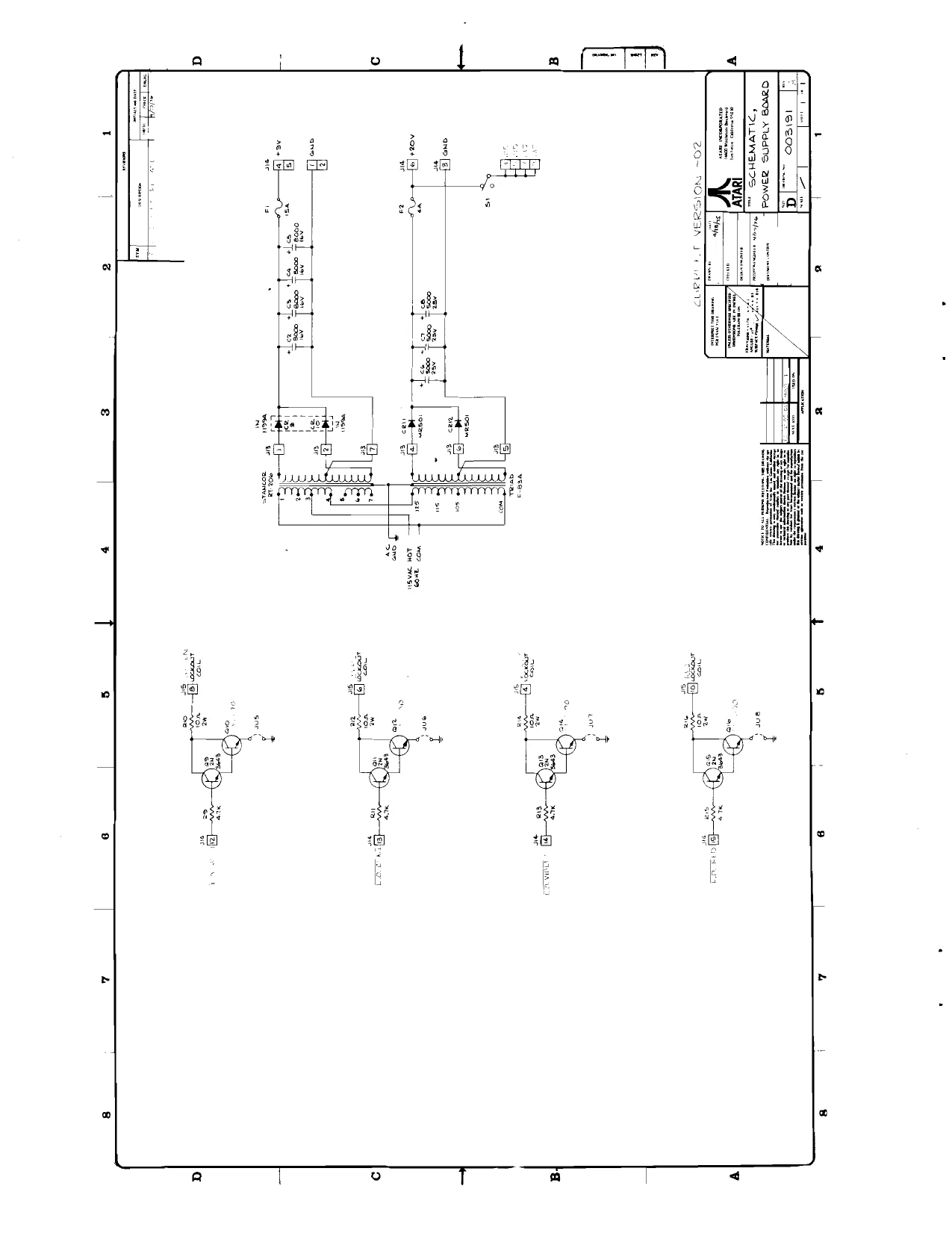
2.6 POWER SUPPLY PRINTED CIRCUIT BOARD
The power supply board has the circuitry for the unregulated supplies and for driving the coin mechanism lockout coils.
The unregulated supplies are both full-wave center-tap rectified configurations. The +9V supply may vary from 7.5V to nearly 11V, depending on line voltage at the transformer primary and the load current. It supplies the power for the +5V regulators on the logic PCBs. The +20V supply may vary from 8V to 22V, again depending on line and load conditions. It supplies power for the audio electronics on the car boards and for the lockout coil drivers.
The lockout coil driver should be active when the LOn signal is high, i.e., when car n does not yet have credit. This causes switching transistor 2N3643 to tum on power transistor 2N5190, allowing current to flow through the lockout coil. This enables a coin to be entered. The entry of a coin for car n causes LOn to go low. This signal going low turns off the 2N3643, and the latter device then turns off the 2N5190. The lockout coil is released by the 2N5190, and further coins are locked out until the end of the present game, i.e., when LOn goes back high.
DIRECTION CODE HORIZONTAL INPUTS (H3) VERTICAL INPUTS (K3) D4-D1, RO OCBA DOCBA wee occ cc coco cc ccc0e Bot eco oO OOOH ccc c000 SoS ISS aS Sate SSS Soo 6 Som, 0000004 -cec0CC CODCOD CCC CCCC0000 Bs 0 OH COO C COSC COCO OOO— een 0 007-000 -c00000000+--0 340024005400 +400+-00--00--00--c0 0407070207970 04050-0-070-0+0+0 Bt 006 HH HO 0 0 OG OHO HOU SSeSeece see Seeeo soo ooo ao. Sooeege ese ias Soro ers toecoces —— Os 000-00 0000000 ++000+---c0 634g 36 6 So Be SO Sse aa
STOP CODE 0100 1000
Table 2-1: Unit Motion Codes for All 32 Directions
III. ADJUSTMENTS AND SERVICING
3.1 OPERATOR ADJUSTMENTS AND OPERATING INSTRUCTIONS
3.1.1 ADJUSTMENTS: There are several adjustments available to the operator. These are:
@ Master volume switch (on sync PCB) e@ Game time adjustment (on coin control PCB) e@ Lockout coil power switch (on power supply PCB)
The master volume switch adjusts the overall audio volume level to one of four possible levels. It is located on the sync PCB as shown in Figure 2-1. Clockwise adjustment decreases volume; counterclockwise adjustment increases the sound level. All of the car PCBs have their own separate volume controls. These are preset at the factory for balanced output levels, and should be changed only by service personnel making repairs or adjustments to the car PCBs.
The game timer potentiometer is located on the coin control PCB in the upper corner near the front of the card rack. It adjusts the length of the game from approximately 75 seconds to nearly three minutes. Game time is increased by turning the pot downward or clockwise, as seen from the front of the card rack.
The lockout coil power switch is located near the edge connector of the power supply PCB. If switched to the “off" position, all of the coils will go into the coin lockout mode, and the machine will not accept coins. In order to use the coin mechanisms in the machine, this switch must be in the "on" position and power must be on.
3.1.2 OPERATING INSTRUCTIONS (UNATTENDED OR AUTOMATIC MODE): After insuring that the machine is properly assembled and secure, apply power by inserting the power plug into a 105-125 VAC, 60-cycle, three-pronged or grounded receptacle rated for at least 5 amperes (600 watts). It will take a few minutes for the TV monitor to warm up. The game should come on in the attract mode (no sound or car motion). A coin in any slot will increment that coin counter, cause the lockout coil to engage, and reset that car to the starting line.
After approximately eight seconds, the game will start: sound will come on and the cars may be driven. All cars that have not received credit will disappear from the TV screen. The eight-second delay allows all players to deposit their money before the game SUantS——Any_pleyer-GepeSiting Winy after the vane starts will also get his car reset to the starting line and may play for the remainder of the game.
3.2 SERVICE AND TROUBLESHOOTING
Indy 4 is sold with one spare PCB for each kind of circuit board in the card rack, and one spare steering PCB. When inserting circuit boards into the card rack, take the following steps to insure that the game will not be damaged:
3.2.1 Be certain that the board is the proper type for that position and that it is not reversed. See Figure 2-1 for location of board types. Heatsinks should always be at the top of the board and to the right.
3.2.2 Be certain that the board is inserted straight into position in the card guides.
3.2.3 Pushing gently, wobble the board slightly until it begins to seat into the connector. If it does not begin to seat, recheck the above two steps, and check for warpage of the board. Correct any problem.
3.2.4 Applying firm, constant pressure, push the board into place until it is seated fully. The front edge of the board should be flush with adjacent circuit boards. DO NOT use fast, jerky motions, as this could damage the backplane board or the edge connector.
When removing boards, always use the card ejector tool provided with the game. Hook the bolt of the tool into the hole in the uppermost corner of the circuit board. Using the frame of the card rack as a pivot, pull gently up to disengage the card from the backplane (see Figure 2-8). Remove the ejector tool, and pull the card out by hand.
When troubleshooting, the short description of each board in Section II of this manual should help in quickly locating a problem. Replacing a suspect circuit board with a replacement gives quick verification of the source of the problem. To fix a circuit board, refer to the schematic and technical description provided in this manual. Repair of circuit boards should be attempted only by qualified technical personnel with proper equipment. As an additional aid to maintenance, the system has been designed so that all four car PCBs are interchangeable. Also, removing one car board will only disable that car, without affecting any others.
Card Guide
Card Rack Rail
Card Ejector Tool
Printed Circuit Board
Pull Out Gently
Hook End of Bolt Into Hole
Figure 3-1 Use of Card Ejector Tool
3.3 TEST EQUIPMENT
In order to test any Atari PCB, same items such as the logic probe are absolutely essential. Others are desirable and will make the test procedure easier, but are not absolutely essential. Some of these instruments are available from the Atari Customer Service Department and are: the Kurz-Kasch 520 Logic Probe, the Atari Video Probe, and the Hewlett-Packard 10529A Logic Comparator. Other instruments that are very useful are the HP 10526T Logic Pulser and the Tektronix 465 Oscilloscope. These two items are available through your local electronics supply house. You may write to the Customer Service Dept. at Atari, Inc., 2175 Martin Avenue, Santa Clara, CA 95050 or call at (408) 984-1900.
3.4 REQUIRED EQUIPMENT
The following items are absolutely essential to perform the test procedures presented in this manual.
3.4.1 LOGIC PROBE: The logic probe is an instrument designed for checking the outputs of integrated circuits. The Kurz-Kasch Logic Probe, Model No. LP-520, which is available through the Atari Customer Service Department or most large electronics supply houses, is recommended. This logic probe is indicated if a signal is logic high, logic low, or changing from one state to another. Consult the operating instructions included with the probe for further details about its operation.
3.4.2 VIDEO PROBE: The video probe is a very simple but extremely useful device, and consists of two test clips, a length of rubber-coated test lead wire, and a 4.7K, k-watt carbon resistor. Video probes may be obtained from the Atari Customer Service Dept. or, if necessary, they can be assembled from standard components available at all electronics supply houses.
3.5 OPTIONAL EQUIPMENT
It is possible to find 90% of the possible PCB computer malfunctions without the following items. However, if a complete set of troubleshooting equipment is desired, Atari recommends:
3.5.1 HEWLETT-PACKARD 10529A LOGIC COMPARATOR: This device is used to verify correct IC operation. This device simply clips onto in-circuit ICs and instantly displays any logic state difference between the in-circuit test IC and the reference IC in the comparator. Logic differences for each pin of a 14 or 16 dual in-line package (DIP) are indicated by a lamp on the comparator. If the logic comparator is purchased form the Atari Custamer Service Dept., it is shipped with 20 preprogrammed reference PCBs. If the device is purchased elsewhere, these _ PCBs must be specially programmed.
3.5.2 HEWLETT-PACKARD 10526T LOGIC PULSER: This device is used to stimlate in-circuit ICs, so that they ere driven to their opposite states. This device is available from the Atari Customer Service Dept. or can be obtained from most large electronics supply houses.
3.5.3 TEKTRONIX 465 OSCILLOSCOPE: This scope is used for viewing various wave forms, and should be ordered from Tektronix. Consult the manufacturer's operating instructions for details on oscilloscope operation.
3.6 LOGIC TYPES AND FUNCTIONS
Type
7400
7402
7404
74804
7408
7410
7413
7420
7425
7427
7430
7448
7450
7474
7483
7486
7490
7492
7493
74107
74153
74157
74165
74192
74193
1bB80
NE555
NES66 Function
Quad 2-input NAND gate
Quad 2-input NOR gate Hex inverter
Hex inverter
Quad 2-input AND gate
Triple 3-input NAND gate Dual NAND Schmitt trigger
Dual 4-input NAND gate
Dual 4-input NOR with strobe
Triple 3-input NOR gate
Single 8-input NAND gate
BCD to 7-segment decoder Dual AND/OR gate (inverter/expander)
Dual D flip-flop
4-bit full adder
Quad exclusive OR gate
Decade counter
Divide-by-12 counter
4-bit binary counter
Dual JK M/S flip-flop
Dual 4-bit multiplexer
Quad 2-input data selector/multiplexer
Parallel-load 8-bit shift register
Synchronous decade up/down counter
Synchronous binary up/down counter Amplifier . Timer
Function generator
Type
RC4136D
MFC6040
8098
8103
8099
9311
9312
9314
9316
9321
9602
74186 Function
Dual operational amplifier
Quad operational amplifier Voltage-controlled operational amplifier
Hybrid
Hybrid
Hybrid
One-of-sixteen decoder/demultiplexer 8-input multiplexer
Quad latch
4-bit binary counter
Dual one-of-four decoder
Dual monostable multivibrator
Read-only memory (ROM)
This page carries no recoverable text. It is a drawing or a photograph. See the original scan.
IV. SCHEMATICS, PARTS LISTS AND DRAWINGS
Number
A004793
A004792
A005082
A004797
005488
005480
A005486
001151 000607
003000
A003184-02
A003170-02
A003182-02
A003199
A003191-02
(none) Title
Parts List and Drawing Cabinet Top Assembly
Parts List and Drawing Cabinet Lower Assembly
Parts List and Drawing Dashboard Assembly
Parts List and Drawing Double Foot Pedal Assembly
Drawing Harness Installation
Schematic (Wiring Diagram) Harness
Parts List and Drawing Electronics Tray Assembly
Schematic, Steering PCB Parts List and Drawing, Steering PCB
Schematic, Parts List and Drawing Car PCB
Schematic, Parts List and Drawing Coin Control PCB
Schematic, Parts List and Drawing Score PCB
Schematic, Parts List and Drawing Sync PCB
Parts List and Drawing Backplane PCB
Schematic, Parts List and Drawing Power Supply PCB
Schematic G.E. Color TV, Chroma Input PCB
Part Number DESCRIPTION
004578 2 004579 3 004580-01
5 75-99090006 6 82-8014B
8 75-5524NX 9 75-0158 10 75-915S 1 004605 12 005138-01
14 75-045
16 005081-01 or 02
17 A005082 18 78-6900401 19 A005482 20 75-07021 A/R
- Optional: Double Cgated Scoth Tape P/N 78-603116 Top Cabinet Base Screen Cover
Well-Nut, Blind Hole Fastener Screw, Button Hd, Socket Cap, 10-32 x 7/8" Lg
Bolt, Carriage, Rd Hd, Sq. Neck, Stl, %-20 x 15 Lg Washer, Flat, Plain Pattern, #% Nut, Mach, Hex, STD Pattern, #4-20 Bracket - Canopy Pole Bezel, 25" Monitor
Washer, Split-Lock, Cres, #%
Instructions - + 005081-02 to be used without Dollar Bill Acceptor Dash Board Assembly Tape, Foam, Adhesive Approx. 15'-0" Top - Steering Harness Nylon Black washers
JA| PROO_ RELEASE fe fey Fem can 780 ard | Rev Pe EN 2473 pr
INSIDE TOP BOLT HEAD Is
_-~-@ rer
A SOL SLREEN CORR UH FORMA TAFE SEL RUNG AOMDER SOS GETORE AXCENTER INSTRUCTION $ CONTROL CAROS “ ~ ner
APPROX. AS SHOWN ner yp
OOS08I-O wir BLL ACCEPTOR COSOBL-OL WrTHOUT BILL ACEPTOR os Ay DOUBLE SIDE TAPE AS REQUIRED.
PIN 18-G7O1CT SECTION "B-B"
INDY 4 an? Innovative leisure CABINET ASSEMBLY , LOWER P/ 004792
Page 1 of 2
Rev. A | 5 [Rev per ECN 2463 [ 4722775, [Cc [Rev per ECN 2502 4/26/76 a | Description Description
DESCRIPTION
1 5" Arkay Speakers
| 2 | 004723 | 1 | Panel, Left Side |
| 3. | A003637 -12 | 2 Coin Door Assembly |
| 4 | 000869 | 4 Alum. Speaker Mesh Cover |
| 5 | 73-77004 | 16 Rivets, 3/16 x .68 Lg |
| 6 | 004724 | 1 Panel, Right Side |
| 7 | 72-6810 | 16 | Screw, Self-Tapping, #8 x 5/8, Phil, Pan Ha |
| 8 | 75-5124B | 12 | Carriage Bolt, #10-24 x 1: Lg |
| 9 | 75-010S | 12 | #10 Flat Washer |
| 10 | 75-040 | 28 | #10 Lock Washer |
| 11 | 75-911S | 20 #10-24 Hex Nut |
| 12 | 72-6812 | 32 | Screw, Self Tapping, #8 x 3/4, Phil, Pan Hd |
| 13 | A004778 | 1 | Frame Weldment |
| 15 | A004797 | 4 | Double Foot Pedal Assembly |
| 16 | 72-5524 | 4 Scr, Mach, Hex Hd, Stl Cd Plate, #%-20.x 14 Lg |
| 18 | A005173 | 4 |€nclosure, Foot Pedal |
| 19 | 75-5516B | 8 Bolt, Carriage, #%4-20 x 1" Lg |
| 20 | 75-045 | 14 |Washer, Lock, Split, #% |
| 21 | 75~915S | 10 | Nut, Hex, Steel, #%-20 |
| 22 | 78-3201 | 4 Adjustable Swivel Guide |
| 23 | 68-001 | 2 Interlock Switches |
| 24 | 72-5512 | 2 Screw, Mach, Hex Hd, Stl, Cad Plate, #4-20 x 3/4" Lg |
| 25 | 75-025S | 2 |Washer, Flat, Plain Pattern (Narrow), #% |
| 26 | 71-803 | 1 | Assembly, Control |
| 27 | 71-801U1 | 1 Assembly, Transport |
| 28 | 71-802U1 | 1 Assembly, Stacker |
| 29 | 72-1608 | 6 |Scr, Mach, Pan Hd, CRES, #6-32 x i" Lg |
| 30 | 72-1610S | 2 Scr, Mach, Pan Hd, Rec, #6-32 x 5/8" Lg |
| 31 | 75-016S | 8 |Washer, Flat, #6 |
| 32 | 75-046 | 8 Washer, §plit-Lock, #6 |
| 33 | 75-916S | 8 | Nut, Hex, #6-32 |
| 34 | 004086 | 1 Bar, Cross |
| 35 | 72-5108 | 16 |Scr, Mach, Hex Hd, Steel, #10-24 x 1/2" Lg |
| 37 | 75-010S | 8 |Washer, Flat, Reg Pattern, #10 |
| 39 | A005666 | 1 | Assembly, Monitor Frame |
| 40 | * 003195 | 1 44 Pin Extender Board |
Part Number
*003197 78-0901 78-0902 72-6612 002974-01 46 002974-02 47 |*A003000 48 |*2003184-02 49 |*A003170-02 50 |*A003182-02 51 |*A000607 52 | A003199 BP
53 003517 54 003518 55 | A005486 56 { A003191-02 57 | A005238 58 005480 59 | A005481 60 | A005483 61 | A005484 Eo] PRRPPO RPP A BRPENNNUPE ANE
mh ASSEMBLY TITLE CABINET ASSEMBLY, LOWER P/L ao04792 PARTS LIST SPECIFICATION [rage 2 of 2 _|
DESCRIPTION
86 Pin Extender Board Card Rack Ket CR2966 Connector Support Rail CR1407 Self-Tapping Screws, #6 x 3/4 Pan Hd, Sht Mtl Angle Bracket Angle Bracket Car Boards Coin Control Boards Score Board Sync Board STeering PCB Assembly Backplane P.C. Board Backplane Board Support Bar Fish Paper, Insulator Electronics Tray Assembly Power Supply Board Harness Assembly & Modification Harness Schematic Main Harness T.V. Video Harness Lock Out Power Harness 62 A005485
A005488
- EXTRA BOARDS TO} BE S! Power Supply Harness
Harness Installation
PPED AS SPARED BOARDS
PRoovcrion nevanse |++9} REV PER ECN 2463 Hl CTREV PER EQN 2502 Wi;
( ; gaya nor 7 4 ates SECTION BB -
- 12 REGO
- 12 REC'D ~(B) 16 READ / ii iz REQD
/ 4) apcao / aS
elcid P ~—(28)
i f (6) < (Die ReaD CABINET ASSEMBLY, coer Asst y,
PRODUCTION REL lars] 1B] REV PER ECH acs [avd [C| REV PER EQN 2So2 |40
D 38) 6 reap / (0) © READ SS / @& / Na AY 4 INSERT TABS OF ACCEPTOR ——= WW Wout (2 BLAceS)
-@ / A004792-02 LOWER CAB. ASSY- WITHOUT BILL ACCEPTOR. (a6) 4. AQO#TR2-OL LOWER CAB, ASS'-WITH BILL rd . ACCEI
a NOTE: \— art ¢ RSHT RAILS.
SUPPLIED WITH ACCEPTOR,
\ uses see
‘SUPPLIED WITH ACCEPTOR,
re) vew AWA
Innovative leisure
| item | Part Number | . | DESCRIPTION |
| L | 000598-03 | Ref | Steering Wheel Assy (10" Dia. Wheel) | |
| 2 | 72-11128 | 6 | Screw, Mach, Pan Hd, Phil, #10-24 x 3/4" Lg | |
| 3 | 000567 | 1 | Bow Washer | |
| 4 | 004805 | 1 Backing Plate - Wood | |
| 5 | 004582-xXx | 1 | Plate - Mounting (Alum) | |
| 6 | A000607 | 1 | Steering PCB Assembly |
—~(2) © REQ'D
PARTS LIST SPECIFICATION
Checked Mech. Eng.
Innovative Elec. Eng leisure
| tem | Part Number | Qty. | DESCRIPTION |
| A004798 | 1 | Double Metal Foot Pedal Assy | |
| 004801 | 1 | Mount Board, Foot Pedal | |
| 4 | 002191 | 2 | Foot Pedal Switch Brkt |
| 5 | 65-0 1C | 2 | Switch, Cherry E51-60B |
| 6 | 75-8810 | 5 | Screw, Wood, Flat Head, Steel #8 x 5/8" Lg. |
| 8 | 75-914s | 4 | Nut, Machine, Hexagon, 4-40 |
| 9 | 75-048 | 4 | Washer, Split-Lock, Cres #8 |
| 10 | A003157-02 | L | Foot Pedal Harness |
JA] PRODUCTION RELEASE
ECN NO 2427 ECN NO. 2449
® 2 READ y 2 REQ'D
NOTES: UNLESS OTHERWISE SPECIFIED
This page carries no recoverable text. It is a drawing or a photograph. See the original scan.
A | PRoD REL
~N HARNESSES MAIN A005481-01 TV-VIDEO A005483-01 LOCKOUT POWER A005484-01 POWER SUPPLY A005485-01 j
CONNECTIONS STEERING SPEAKER COIN MECH LOCKOUT COILS FOOT PEDALS ELECTRONICS TRAY POWER SUPPLY BOARD MOTHER BOARD aay y 0 INTERLOCK SWITCH 11 AC POWER TO FAN 12 AC POWER TO BILL ACCEPTOR BILL ACCEPTOR CREDIT OPVNOOSaN-
HARNESS INSTALLATION iD |" d05400 a D
This page reads as a drawing: its text was drawn rather than typeset, and comes out in fragments. See the original scan.
This page reads as a drawing: its text was drawn rather than typeset, and comes out in fragments. See the original scan.
INDY _4 ELECTRONICS TRAY P/L A005486-01|
PARTS LIST SPECIFICATION
Drawn Page 1 of 1
Checked Mech. Eng. JA. ? leisure Proj. Eng. Elec. Eng
005478 2 A005485-01 3 A005164-02 4 42-7112 5 41-2001 6 46-202501 7 79-3201 8 005507-01 9 A004381-01 10 000871-01 11 72-6608 12 72-6612 13 72-6812 DUAKE PEP BPH DESCRIPTION
Electronics Tray Power Supply Harness Transformer, Triad F83A Transformer, Stancor RT-206 Filter Power Line Fuse, 5 AMP Fuse Holder Electronics Tray Cover Power Cord 8' Assy Label Screw, SM, Pan Hd, Phil #6 x 4 Lg “ wow mH Be x 3/4 Lg " moomoo 8 Ee yx 374 Lg
PROD REL
REV PER ECN 2504
A005486] 1/1 B
L-O@ ance) ean ‘OUTSTANDING ECN) rs | CURRENT VERSION A00548G-01
DO NOT SCALE
DRAWING
ELECTRONICS
TRAY ASSEMBLY
UNLESS OTHERWISE SPECIFIED
LED MENI24
NOTICE TO ALL PERSONS RECEIVING THIS DRAWING CONFIDENTIAL. Reproduct
NEXT ASSY KOO COT [next Assy] season Be Swing panel or te ign en this
MICRDFARADS.
- ALL CAPACITINRS |) YAW, 5% CARBON.
ALL RESISTORS IN) OHMS,
NOTES: (UNLESS OTRERWIE SAL)
ATARI INCORPORATED 14600 Winchester Boulevard
‘TOLERANCES: ATARI Los Gatos, California 95030
FRACTIONS = 21/16 ANGI SURFACE FINISH ~
suzt | DRAWN, No REY. B | Qos C SCALE NONE] ser oF Y
KUse Job Title paceTRAK STEERING PCB ASSY Dw8-P/L 000607
a. Drawn t lof 1
Checked
Proj. Eng Mech. Eng. Rev.
Elec. Eng. — ATARI
| Rev. | Description | Apprv. |Rev. | Description |
| H | Redesigned | 538-74 |
J Rev_ per ECN 397 5/28/74 K__|Rev_per ECN 457 6/3/74 L Rev per ECN 601 7/15/7! M Rev per ECN 1531
| Item | Part. No. | Qty | Description |
| 1 | 000614 | 1 | Printed Cipcuit Board (E) |
| 2 | 001092 | 1 | Light Noun |
| 3 | 001151 | Ref | Schematic Diagram |
| 4 | 11750/10-5750 | 2 | Resistor, Comp., 75 ohm, % watt, 5% |
| 5 | 11471/10-5471 | 4 | Resistor, Comp, 470 ohm, % watt, 5% |
| 6 | 11332/10-5332 | 2 | Reslistor, Comp, 3-3Kohm, % watt, 5% |
| 7 | 34104 /27-101103 | 2 | Capacitor,| Ceramic, .Oluf | |
| 8 | 70006 /38-2N5777 | 2 | Transigtor|, 2N 5777 (Photo Darlington) |
| 9 | 70000/34-2N3643 | 2 | Transigtor|, 2N 3643 |
| 10 | 71008/38-ME7124 | 2 | Light Hmitfting Diode, I.R. ME 7124 | |
| 14 | 80089 /79-58005 | 1 | Connector} 10 pin, PC Mount, Amp #1-380991 |
| 15 | 72-12128 | 1 | Scyew, |Machine, Pan Head Phil, #2-56 x 3/4 Lg. |
| 16 | 75-042 | 1 | Washer eit Lock #2 |
| 17 | 75-9128 | 1 | Nut, Hex, }#2-56 |
| 18 | 003749 | 1 | Retainer, [Led Light Mount |
fe ee Pee Eon Gor_|red MODIFICATIONS + FOR OCOOCIA REV J P.C.BOAZDS \, JUMPER FROM PIN 2 TO PIN IO OF THE 10 PIN CONNECTOR,
ON CieeuIT SIDE OF BOAeD,
- JUMPER FROM PIN. 1 OF THE IO PIN CONNECTOR To THE
PAD MARKED +5y (END OF 21) ON CIRCUIT SIDE OF BOARD,
MODIFICATIONS : FOR OCOOSI4 REV K P.C.BOAZDS. }, JUMPER FROM PIN 2 TO PIN IO OF THE [0 PIN CONNECTOR,
ON Cie@cLiy SIDE GF BOARD. a ATARI INCORPORATED
14600 Winchester Boulevard
ATARI on ‘aussi 30
mE
ASSEMBLY
STEERILUG BoARD
aTTeACT
atrract[ig] iE couuision je tre
orezeinel
tf 2F aF OF
+9
eNO a] low wees vac (BEB wv av a cae neers Ss
moroe Feeavency srvesct aos Pore be | BAC en2
cee
wore
ey 5 a ZeCUSON 5 = 2 2 COLLISION Fy 1 a Teeser_¢ Ble oh St u1 N RESET- ce z S. o| SES 7 fs ee Ts cae 6 E 12lo0. zy eat ct d+ 4} Shee al i T -o1 raoet 22 Ol
ier venom TNACS it ATE re TT PRODUCTION RELEASE
REVISED PER ELN 11GG REVISED PER EQN 248,203 REVISED PER ECN 1SDI has REVISED PEG EQ 1428 haa REVISED PR EC! S02 ad
wer
Moror. euoeN x
x
003629 (serecren| “NS )
2+ aa 'g
me the ev
aH SER
2a. Tole, pe ces
- + &
P+
- 4 |5 je jo eco erp” |e ST OB le Sh os acap me wayyy +
aaat 4 cociee <a ceezer_ ial cvock , easy ZEN p12 i ial 10
+
io] KT 8. vr t aie we
Tore
Master, Vou. o
Master, Vou. 4
Master Vou. 2
“RSS onan ICID 2! ca [ee oo ech cd ars B [ees [se fe e3 [eee
can 2 fpf fia] RE To MOTHER BORED
ceo cao +204 wide 4001
co
iv “ 10 = +{/_{ia] auoio out errs
ATARL INCORFORATED "eg Wechsler Un Grom Corn 5050
SCHEMATIC CAR BOARD pI 008000]
Drawn
Proj. Eng. 2/2/75 | Elec. Eng, 2/3/75 | REV. Innovative leisure
| PROD REL | 23-75 | [6 [Rev Per EN Howe [277-75] Lc [Rev Pee ecn 1248, 1269 [Shshs_| | D [eev cee EN SST ts] Je [Rev cee Ew 1428 [Siahs | Rev. Per. ECN 1902 [en/ng |
DESCRIPTION
Printed Circuit Board Heatsink, Wakefield #680-.75A LM309K Positive 5-Volt Regulator LM340T-15 Positive 15-Volt Regulator 7400 Integrated Circuit " Part Number
002999 78-06004 37-LM309 37-LM340T-15 37-7400
| 37-7402 | 7402 | " | |
| 37-7404 | 7404 | " | " |
| 37-7406 | 7406 | " | a |
| 9 37-7410 | 7410 | " | : |
| 10 37-7414 | 7414 | " | " |
| 11 37-7420 | 7420 | 7 | " |
| 12 37-7474 | TH74 | " | " |
| 13 37-7475 | T4758 | 7 | " |
| 14 37-7485 | 7485 | " | = |
| 15 37-7430 | 7490 | " | = |
| 16 37-7492 | 7492 | " | " |
| 17 37-7493 | 7493 | » | " |
| 18 37-74107 | 74107 | " | " |
| 19 37-74153 | 74153 | " | " |
| 20 37-74193 | 74193 | x | 7 |
21 003186 ROM, RT8 Car Video, 512 x 8, 4096 Bit 22 003187 P-ROM, RT8 Motion Code, 32 x 8, 256 Bit 23 37-9312 “24 37-9316 25 37-555 26 37-LM324 27 37-LM380 28 34-2N3565 29 003629 30 35-2N3644 31 31-1N914 32 38-MV 5013 9312 Integrated Circuit
| 9316 | " | " |
555 Timer Integrated Circuit LM324 Quad Op Amp LM380 Audio Power Amp Transistor, NPN, Type 2N3565 Transistor, Noise Source, 2N3643 Transistor, PNP, Type 2N3644 Diode, Type 1N914 Light Emitting Diode, Visible, Red NOPR EEE NOPE HP OPNEP EP EN EER RON ERR EH
35 | 19-315103 36 | 10-5151 37 | 10-5102 38 | 10-5152 10-5332 19-5472 10K ohm Trimpot Resistor, Carbon, 5%, %W, 150 ohm pRj,2
| " | " | mB 1K ohm R3,4,7,13,45-f7 |
1.5K ohm R42
| " | " | " " 3.3K ohm R43 |
| " | " | " " 4.7K ohm R29-36 |
OrPRANE
INDY _800
ASSEMBLY TITLE RT8 CAR BOARD | _PARTS_LIST SPECIFICATION REV. F Page 2 of 2
DESCRIPTION
10-5103 10-5123 10-5153 10-5333 10-5683 10-5823 10-5104 10-5224 10-5474 10-5105 10-5225 10-5475 19-315254 28-101101 27-250103 21-250103 27-250104 21-250104 29-011 24-250105 24-250505 24-250106 24-250507 72-14128 75-9168
75-056 31-1N4001 78-16005 RNP EN EN EN PEEP EP PNNNAIEP PEPER O Resistor, Carbon, " "
250K ohm Trimpot P/L A003000
3cW " 10K ohm 12K ohm 15K ohm R48 33K ohm 68K ohm 82K ohm R5 100K ohm R14-20 220K ohmRri2,41 470K ohmRll,40 1M ohm R10,39 2.2M ohmrg 4.7M ohm R9 R21-28, 44
Capacitor, Mica, 100pf, 100V " Ceramic, Film (Mylar), Ceramic, O.luf, 25y Film (Mylar), Monolythic, 0 Electrolytic, Electrolytic, Electrolytic, Electrolytic, Serew, Mach, Sht Mtl, Pn Nut, Machine, Hex, 6-32 -Oluf, 25y -Oluf, 25V
O.luf, 25V 22uf, 12V luf, 25V Suf, 25V 10uf, 25V 500uf, 25V Hd, Phil, 6-32 x 5/8"
Lock Washer, Internal Star, #6 Diode, IN4001 Silpad
This page carries no recoverable text. It is a drawing or a photograph. See the original scan.
sym orscrion ear [amex | nme Bleeviseo pee cen er [Me } € [Revise Pee een 1428 [Ph F |Revises PER EG S07 [iene
°
3} <
gs z fay cd <
a ra < uo
NOTES:
- LED's TO BE MOUNTED POINTING TOWARDS BACK OF BOARD AND LAYING CowN.
- THIS ASSEMBLY To BE USED WITH 007989 RENISIONB" P.c. ROARS
MODIFATIONS. | (TO REVISION "BI AND KEVISION €’ 002289 RasenS). LINSTALL TWO IN@OO! DIODES WW SERIES AS SHOWN, CUTTING TRACE UNGEZNEATH EACH BIODE,
Z.INSTALL (Oat 25U CAPACITOR AS SHOWN STANDING UP.
MOBIFICATION ; (To REVISION "A COZS99 BoAeDs ONLY)
- CLT TRACE AS INDICATED. JUMPER + (PosiITUE) END OF 17 (lout /25y) CAPACITOR TO DS PIN 2 (LWB24)-
ATARI INCORPORATED 14600 Winchester ATARL
m™ ASSEMBLY, 29 WR 75, Soa ere aes umes reo CAR BOARD
AOGBOOO | [7A ee Ge
GREEN See Lclagt B toe’
evan) con Fi
PLAY TIMER
Pr ATTRACT pW sy GREEN JoK 2)
Peay EFAS _ Q BREEN
a oat
YioLeT COmy 33 ATTEACT
"s ict
RED po sy LET
ose or aurenna [4
sv
2] im
VSYne, +s
R49
R55 OREN joe eow
| orden | Lipo 2 | ., Lean |
| CAR | i[Sa)? 18 | | |
ye. 4 262eEN —SAR\e 2h
| 7a | ceeorT —41ca) | Pgaey | 1 |
c4e cezen Ses]
| e | ese | CYAN | |
| ua | aE | xan | it |
3 ia
| eyaw | she | fh | vo |
- ALY
| CAR | y pales | hic |
CYAN 2 fAS\e se[58
| 1 | veo)? 2438 | Pag | |
| . | cre evan | "Fal | |
| — | 57 | vouer | |
| 2 | zt; Less | ioe | tons |
ioe cae eco a 4 oe ®
Buo\Game 260 Lup vol 5; ae ape 3
| CAR | ti 4lbe | 2 | 4 |
2 = areal a
| END game | c4cvir 158, | as) | BS |
25y cre reo 2{c74 ale
| dese | | | 7 |
| : | bey | I |
sil P
Stoke RESaT
Ker | fee YD V a D
MONO END GAME ‘as ~~ en 3644 4 @ * e59 , 2 ol 1K
os Tels
ate] [lalelo
| b | +94 | “as |
8a Sk
g §8 sore i ars cer tae
Sets perme re Soe eet ISR rete i fe ee a meee RES i ne
| . | ese | | g |
Mone 250 o7
BY PASS
uD TO BOARD +SY TO BoARD, A | PROBUGT/ON RELEASE
car RESET GREEN
CAR Reser Cran
“se
CAR RESET wover
cae RESET RED
LAST REF BES
R59 rd cke7 @3 &
WOTES : 1 ALL DIODES ARE INN4.
CURRENT VERSION -02
SCHEMATIC , COI CONTROL BOARD
PARTS LIST SPECIFICATION
Checked
Innovative leisure
Description PROD. REL.
Part Number ye DESCRIPTION
| ] | 003185-01 | 1 | Printed Circuit Board | |
| 2 | 37-LM309 | 1 | LM309K Positive 5-Volt Regulator | |
| 3 | 78-06004 | 1 | Heatsink, WakeField 680-.75A | |
| 4 | 72-1610C | 2 | Screw, Machine, Pan Hd., Phil., 6-32 x 5/8 | |
| 5 | 75-916C | 2 | Nut, Machine, Hex, 6-32 | |
| 7 | 75-056 | 2 | Lock Washer, Internal Star, #6 | |
| 8 | 37-7400 | 2 | 7400 1.C. | E4,F4 |
| 9 | 37-7402 | 3 | 7402" | HI, A2, B2 |
| 10 | 37-7404 | 6 | 74o4 | Cl, El, Fl, £2, |
D5, F5
| W | 37-7408 | 4 | 7408 =" | Al, Bl, A5, B5 |
| 12 | 37-7410 | 1 | 7410" | c2 |
| 13 | 37-7430 | 1 | 7430" | c5 |
| 14 | 37-7474 | 4 | 7474 8 | A3,B3,C3,A4 |
| 15 | 37-7493 | 2 | 7493" | Jt, Kl |
| 16 | 37-74164 | 1 | 74164 | ch | |
| 18 | 37-555 | 555 Timer 1.C. | Ll | |
| 19 | 37-LM339 | LM339 Quad Comparator | E3, J3 | |
| 20 | 34~-2N3565 | Transistor, NPN, Type 2N3565 | Qi, 2 | |
| 21 | 31-1N914 | Diode, Type IN9T4 | CR8,9, 13-27 |
22 ~e 23 .
| 24 | 10-5102 | Resistor, Carbon, 5%, 4W, 1K OHM R41,46,48,59 |
25 | 10-5103 " HHH Toy ony -R13,23,28, 33,38 55-58
ASSEMBLY TITLE 'NDY 4 COIN CONTROL BOARD P/L 4003184-02 PARTS LIST SPECIFICATION REV A “TTrage 2of 2
DESCRIPTION
10-5104 5 Resistor, Carbon, 5%, 4W, 100K OHM R12,22,27,32,37 10-5224 220K OHM = R43,44 10-5221 220 OHM R47 10-5274 270K OHM R11,21,26,31,36 10-5394 390K OHM R49,50 19-315105 Trimpot, IM OHM, P.C. Vert. Mount R42 24-250105 Capacitor Electrolytic, | uf, 25V C28 24250227 " " 220 uf, 25V C37 29-008 Capacitor, Ceramic, 0.1 uf, l2v, 20%, C10,16,20,23,26
| 27-250102 | Capacitor, Ceramic, .O0luf, 25V | C33 | ||
| 27-250104 | “ | " | O.luf, 25V | €14,17,18, 21, |
24, 29,30,32,35 38-2
29-011 Capacitor, Monolythic, .22uf, 12V, Rad. C34,36
| 33-2N3644 | Transistor, PNP, 2N3644 | Q3 |
75-0168 Washer, Flat, Reg. Pattern, #6 Steel 78-16005 Silpad
This page carries no recoverable text. It is a drawing or a photograph. See the original scan.
ware [ower [on B [PRODUCTION RELEASE 11237
NOTES: J. THIS ASSEMBLY DRAWING TO BE USED WITH 003185 REV ‘B! P.C. BOARD.
- ALL DIODES ARE INDIA,
MODIFICATIONS: (TO BE DONE TO 003185 REV '3' P.C. BOARD)
- ON CIRCUIT SIDE. CUT TRACE BETWEEN PINS 8 AND 9 OF C5, AND CUT L-SHAPED TRACE GOING TO PIN B OF C5,AS SHOWN:
CUT BETWEEN 8 & 9 goto ees S 5 “or 0000000 CIRCUIT SIDE SHOWN
2 BUMPER EDGE CONNECTOR PIN 'P/TO FI PIN 3
- cut & urT FI INGO. JUMPER J4 DIN 9 TO €4 PIN 1\4)10 £13. VUMPER CS:PIN | TO PIN 24 PIN3 TO PIN 43 PIN 5S TO PIN &: AND PIN li TO PIN AZ, 6 CUT & LIFT DS PING. 7% JUMPER DZ: PIN 3 TO PIN4; PIN @ TO PIN 7: AND PIN \3 TO PIN i2.
- GUT AND LIFT C2 PINS. S. JUMPER C2 PIN 13 TO FI PIN: 4. ae
rnin
CURRENT VERSION -02
ASSEMBLY s COIN CONTROL BOARD
‘SCORE _RESET as|
£393
is |e IF 4D 4 4F
Tle len Jee ye
Scone RESET
250M
ea. 18v. yp lelsle Te se 32 °
le [pie Tels
a3 93 AB ¢ > Tep [8 |7 7 80 BE BF Z as 2} 8
Score winoow ES) FLASH sey © 32H x] [2] p_4for 3_No LEAceR a [z Lenoer ror ° @3l!2 Leaner roe 4 cenven £03 :
4 xara e ap, * a a1. wl £ lng asl, LEADER 103 77 ee I LEADER DZ Tae SG Leaver Tot Ici ko Ea no LEADER: 31S a —je 2 [sis Sfarg* 5 Ae As AZ 8 zlaea “F EA 8 sli fia ye
2564—— os (2a
By av (iti bbhdde SUR Made escaaron
apare
2| 3] rs
Tel
ray —| lv 2seH +sv ro TV
/3bp ba SED 8p VES. ig a] (waite) +5v Re ZF ar] A} (OEE oy ie sy p rea
OLE CAR viveo ioe eae wioeer)
REO CAR VIDEO RED SCORE (rep)
GREEN CAR viDEO y GREEN SCORE (GREEN) ‘
| tyan eae 12 | spae)t | tn] Moe |
¥ ies ED (eran)
DUMPER POSITIONS
bone = Back scemen OO | = DOT PATTERN O72 + wHiTe sceeeN O70 3 = NORMAL P I> pole
| T | 13 | T | +7 70 goARD |
| 6 | +e | Cae | |
| ee | 77250 | OF ’ | |
| Mono | ik | [ores |
sup To BoKeD
3fe tl4leleo CURRENT VERSION -02
SCHEMATIC SCORE FP. C. BOARD
Inoy 4 ASSEMBLY TITLE SCORE BOARD, P.C. BOARD P/L. a003170-02
PARTS LIST SPECIFICATION
Drawn Checked | ATARI Innovative leisure
Description PROD. REL.
DESCRIPTION.
| 1 | 003171-01 | 1 | Printed Circuit Board |
| 2 | 37-LM309 | 1 | LM309K Positive 5-Volt Regulator |
| 3 | 78-06005 | ] | Heatsink, Wakefield 680-1.0A |
| 4 | 72- 1610C | 2 | Screw, Mach., Pan Hd, Phil, 6-32 x 5/8 |
| 5 | 75-916C | 2 | Nut, Machine, Hex, 6-32 |
6 | 78-16005 1 | Silpad
| 7 | 75-056 | 2 | Lock Washer, Internal Star, #6 | |||
| 8 | 75-0168 | 2 | Washer, Flat, Reg. Pattern, #6 Steel | |||
| 10 | 37-7400 | i] | 7400 Integrated Circuit A6é | |||
| im | 37-7402 | 3 | 7402 | " | " | D2, H6, J6 | |
| 12 | 37-7404 | 2 | 7404 | " | " | E2, B6 | |
| 13 | 37-7408 | 2 | 7408 | " | " | E6, F6 |
| 14 | 37-7410 | 1 | T4IO | “ | 7 | cé |
| 15 | 37-7432 | 1 | 7432 | " | ” | cl |
| 16 | 37-7448 | 1 | TAL | " | " | Fl |
| 17 | 37-7485 | 3 | 7485 | 7 | “ | F2, J2, L2 | ||
| 18 | 37-7490 | 4 7490 | " | " | Ak, Bh, E4, FA | |
| 19 | 37-7493 | 2 | 7493 | " | " | A3, E3 |
| 20 | 37-74153 | 2 | 74153 | " | n | Al, DI |
| 21 | 37-74174 | 1 | TAIT | " | ™ | H2 |
| 22 | 37-74175 | 1 | TAITS | " | " | K2 |
| 23 | 37-9301 | 1 | 9301 | " | " | 06 |
| 24 | 37-9312 | 12 | 9312 | " | " | A2,C2,B3,D3,F3,J3,K3,L3,A5, |
B5,E5,F5
ASSEMBLY TITLE SCORE BOARD, P.C.BOARD P/L 003170-02 PARTS LIST SPECIFICATION REV. A |Jpage 2 of 2 Item | Part Number Qty. DESCRIPTION
25 | 37-9322 9322 Integrated Circuit HI 26 | 10-5102 Resistor, Carbon, 5%, 4W, IK OHM RI, 4 27 | 10-5103 Resistor, Carbon, 5%, 3W, 10K OHM R2,3,5,7,8,12
| 29 | 28-101331 | Capacitor, Mica, 330pf, 100V | c8 |
| 30 | 27-250104 | Capacitor, Ceramic, O.luf, 25V, | C2-7 |
31 | 29-011 Capacitor, Monolythic, .22uf, 12V C9 32 | 24-250257 Capacitor, Electrolytic, 250uf, 25V Cl
| 33 | 27-250102 | Capacitor, Ceramic, 0.00luf, 25v, | C10-14 |
This page carries no recoverable text. It is a drawing or a photograph. See the original scan.
NOTES:
THIS ASSEMBLY DRAWING TO GE USED WITH 003171 REVISION 'B’ PC. BD.
MODIFICATIONS:
- CUT TRACE THAT GOES TO ‘O’ PAD IN UPPER LEFT CORNER OF BOARD.
- JUMPER '0'PAD TO LARGE GROUND TRACE
- JUMPER "3° PAD TO LARGE GROUND TRACE
4 CLT TRACE
§. CUT TRACE
6, CUT TRACE
- CUT TRACE
- CUT TRACE GOING TO EDGE CONNECTOR PIN 20.
GOING TO EDGE CONNECTOR PIN 24.
GOING TO EDGE CONNECTOR PIN x.
GOING TO EDGE CONNECTOR PIN B
GOING TO EDGE CONNECTOR PINT.
- JUMPER EDGE CONNECTOR PIN ¢c4 TOFS PIN 10
- JUMPER EDGE CONNECTOR PIN E TO ES PIN ID
I, JUMPER AS PIN 10 TD C5 PIN 10,
\2. JUMPER B5 PIN 10 TO 05 PIN 10.
- CUT & LIFT Ce PINS 4 & 5 14, JUMPER Cb PIN 4 & 6 TO IK PULLUP (Ra). ‘5. CUT & LIFT Doe PIN 12. 1b JUMPER TRACE GOING TO De PIN (2 TO Dé PIN II.
- BUMPER TRACE GOING TO Ce PIN S TO Fé PIN 12, .001 CAP BETWEEN C5 PINS 1 & 9_
- INSERT
- INSERT:
- INSERT:
- INSERT
- INSERT: O01 CAP BETWEEN C5 OO! CAP BETWEEN U5 -D0) CAP BETWEEN 4S -001 CAP BETWEEN US PINS 5& B. PINS 2 BB.
PINS 3&8. PINS 4&8,
CURRENT VERSION -02 A | PRODUCTION RELEASE faire
ASSEMBLY,
SCORE BOARD LD |Aoos70 | | 7 ee ATARL_ INCORPORATED 14600 Wonca Boulet Us Grom, alfornt 95030
14,318 0HE, ree js |e Js |e Jo a
rebel ys P
we ogee cogs WIOLETY
omer cas (RED) MASTER AUDio.
way Jeet ore sare (arren}
lorwer cars (evant SS, x[2 2/8Z lek oe x 25 me!
RAL REPLACEMENT SPT AL scEN
oust (ascol Se" Sa1b IT acer, OLDE %
maces prea)
maerer soume
(eeFFeE@ED) VRESET
Ban A [PROBOGTION BELEASE
Sov
Tae IDS)s 6455 2 5.
1S > 223 verse Saas Verne
weync
rev Syrapyu ED v2
s
Fe Ya vy a3] en ¥ Nov © 32H
er
en SitH
ence, ae ont t
wee cnece ooss0e Point @ (ensizsy wnece, a S} BON “. lS ole FOr a wes vey Hae Of =] cnece aov lay asl B] cor zSen teas of eee ree day anf] EC wee eau Sas aie ess ve ws) Sees ft edt sce
Ee <1 e+ e\8 pp ee 20 125 wnt aT, Zoo | 2 Te) Vom
rev ° ev a ev av Sov sync V syne ®
ws JUMPER FOR S047 OPERATION
7 EVETS sfeapd
™ SCHEMAT.C, SYNC BOARD
PARTS LIST SPECIFICATION
Drawn. INDY 4
aad leisure
DESCRIPTION
| 1 | 003183-01 | 1 | Printed Circuit Board |
| 2 | 37-LM309 | 2 | LM309K Positive 5-Volt Regulator |
| 3 | 78-06004 | 2 |Heatsink, Wakefield 680-.75A |
| 4 | 72- 1610C | 4 | Screw, Mach, Pn Hd, Phil, 6-32 x5/8 |
| 5 | 75-916C | 4 |Nut, Machine, Hex, 6-32 |
| 6 | 78-16005 | 2 | Silpad |
| 7 | 75-016S | 4 |Washer, Flat, Reg Pattern, #6 Steel |
| 8 | 75-056 | 4 | Lock Washer, Internal Star, #6 |
| 9 | 66-071P4T | 1 | Rotary Switch, P.C. Mount, IP-4T, Grayhil |
#71AF36-01-1-04-N
| 10 | 73-802 | Switch Knob(Raytheon #50-5-1) | |||
| W | 37-7400 | 7400 Integrated Circuit | Al,B2,B3,J4,F5,H5 | ||
| 12 | 37-7402 | 7402 | 7 | " | D2 | |
| 13 | 37-74HO4 | THHOA | " | ” | A2 |
| 14 | 37-7410 | 74IO | " | ™ | 03 |
| 15 | 37-7417 | TAIT | " | " | B5, D5 |
| 16 | 37-7420 | 7420 | u | " | Cl, A3 |
| 17 | 37-7427 | 7427 | " | " | H3, H4 |
| 18 | 37-7437 | 7437 | 2 | c2 | |
| 19 | 37-7474 | 7474 | " | “ | C3 |
| 20 | 37-7486 | 7486 | " | " | Bl | |
| 21 | 37-7490 | 7430 | " | - | J3 |
| 22 | 37-7493 | 7493 | " | " | D4, £4 |
| 23 | 37-74107 | 74107 | " | " . | DI, E3 |
| 24 | 37-74153 | 74153 | " | 7 | F3 |
| 37-9316 | 9316 | Ak, Ba, Ch |
ASSEMBLY TITLE SYNC BOARD, INDY 4 P/L 4003182-02 PARTS LIST SPECIFICATION REV A [rage 2 of 2 Qty. DESCRIPTION
005502-01 1 P-ROM, RT4 Check Points, 32 x 8, 256 Bit &5
| 005503-01 | 1 | P-ROM, Racetrack, 256 x 4, 1024 Bit | Fa | |||
| 28 | 90-101 | 1 | 14.318MHZ Crystal | YI | |||
| 29 10-5331 | 2 | Resistor, Carbon, 5%, 4W, 330 OHM | R5,6 | |||
| 30 | 10-5681 | 1 | " | " | 1 680 OHM | R4 | |
| 31 | 10-5102 | 18 | ul | " | u | "1K OHM | R1-3,7-20,30 |
| 32 10-5103 | 9 | " | - | ” | "10K OHM | R21-29 |
| 33 | 28-101331 | 1 | Capacitor, Mica, 330pf, 100V | cs | |||
| 34 | 27-250104 | 6 | Capacitor, Ceramic, O.luf, 25V | c6-11 | |||
| 35 | 29-011 | 2 | Capacitor, Monolythic, .22uf, 12V | €2,3 | |||
| 36 | 24-250227 | 2 | Capacitor, Electrolytic, 220uf, 25v | ci,4 | |||
| 37. | 37-7404 | 1 | 7404 Integrated Circuit | E2 | |||
| 38 | 79-42116 | 2 | Socket, 1.C., 16 Pin | FA,ES | |||
| 39 | 37-9322 | 1 | 9322 Integrated Circuit | H2 | |||
| *hO 66-091P10T | 1 | Stripswitch, P.C. Mount, EECO, #1A211001G |
XNOTE: Item 40 is to be used only if items 9 & 10 are not available
th N =
Rx K 7490"
93zz 742
74153
7404
or Bx2:74 ol
4 i 740 741
7437 7474)
D 1400
H zy
Fa = Fs ie a vs 7420
&
MT Mn °
n iin
ry
F MN
m © [PROOVETION RELEASE waza
NOTES \OSSTALL ITEM 38 (Ib PIN. LC. So¢KET) IN POSITION F4 AND ES.
- THIS ASSEMBLY DRAWING TOBE USED WITH 003183 REV 'c’ PC. BOARD.
CURRENT VERSION -02
(Lea 70) ATARI INCORPORATED rns "ato Wiehe Boles ~— ATARI ee
BD [aoosie2 | me ASSEMBLY .
SYNC BOARD
PARTS LIST SPECIFICATION Page 1 of 1 ASSEMBLY TITLE / ACKPLANE BOARD 003199
Innovative leisure
SS OR ST Lo [Rev Per etn 1392 A /z0/ax | | t> [Rev Pee ecn 1436 TSfiaizs | a a fa
DESCRIPTION
003200 Printed Circuit Board (Backplane) 79-514222 44 Pin Edge Connector, 156, Dip Solder 79-514243 86 Pin Edge Connector, .156, Dip Solder 75-1408 Screw, Mach., Pan Hd., Phil., 4-40 x %" 75-914 Nut, Machine, Hex, 4-40 75-054 Lock Washer, Internal Star, #4 T3-Siuool CONNECTOR KEY
l< PESSOCTION RELEASE. | ‘@leenses cee ecu 1253 c[viece Pee ens 152,
hore pa, LALL CONNECTORS MUST BE HAND soLDEZED t.. To F.C. BORED. APPLY BEANISON PASM SICAL BOTE To THE THO PLACEE MDICATER, Z Ch AL. REVISION A’ 003700 PC. BOARDS (COMPONELT B18E): BY] V4 ——— 2 ADPLY DENN CARI SlguAL BOT TO THE NE PUNE DICATER, I ON ALL REVISION “€ OO3200 PE BOREDE (MROWENT SDE)- SS 4400 8 cOMMETOE HEN To coun. vB (Orme BO) exrean MS BI GE, | bo | A | 2 2 they sctNEEOOR ORG Me erase kcceme pater SORE ‘8 ue 2 wa oe ats a6 a: MODICATIONS § (TO GEM EID “AT OOB200 PC. RORES, OLY) |, JMPER CONNECTOR JB PIN Y TO CONNECTOR IO Pies BB
@
Hae [=== LATARL mame | ASSEMBLY,
This page is a drawing, shown as the original scan.
INDY 4 POWER SUPPLY P.C.B. L.A003191-02
PARTS LIST SPECIFICATION Page 1 of _]
Drawn ATARI" Checked Mech, Eng. Innovative Proj. Eng. Elec. Eng REV, leisure A
| Rev. Description | Rate fApprv Vv. | Description | Date | rv] |
| A | PROD. REL. | 4/23/76 | ||
| tem | Part Number | qty | DESCRIPTION | |
| 1 | 003192-01 | 1 P.C.B., Indy 4 Power Supply | ||
| 2 | 24-160808 | 4 |Capacitor, Electrolytic, 8000uf, 16V, 85°C 2-5 | ||
| 3 | 24-250478 | 3 | Capacitor, Electrolytic, 4700uf, 25V, 85°C 6-8 | ||
| | | 31-MR501 | 2 |Diode, Type MR501 (3A) | CRIT, 12 | |
| 5 | 31-1N1199A | 2 Diode, Type INI1199A (12A) | cR9,10 | |
| 6 | 78-06006 | 1 | Heatsink, Wakefield 680-1.25 | ||
| 7 | 61-O11C | 1 SPDT Toggle Switch, C & K 7101, | $l | |
| 8 | 10-5472 | 4 | Resistor, Carbon, 5%, dW, 4.7K OHM | R9,11,13,15 | |
| 9 | 13-0100 | 4 |Resistor, Carbon, 10%, 2W, 10 OHM | R10,12,14,16 | |
| 10 | 34-2N3643 | 4 | NPN Transistor, Type 2N3643 | Q9,11,13,15 |
al
| 12 | 34-2N5190 | 4 | NPN Power Transistor, Type 2N5190 | Q10,12,14,16 |
| 13 | 72-1406C | 8 |Machine Screw, 4-40 x 3/8, Stainless | |
| 14 | 75-9140 | 8 |Hex Nut, 4-40 | |
| 15 | 75-054 | 8 |Lock Washer, Internal Star, #4 | |
| 16 | 75-0148 | 8 |Flat Washer, #4 | |
| 17 | 79-58005 | 2 |Connector, 10 pin, P.C. Mount, AMP #1-380991 J13,15 | |
| 18 | 79-3202 | 4 |Fuse Clip, 3AG, Beryllium Copper, Silver Plate, |
Little Fuse #121001
| 19 | 46-2031503 | 1 Fuse, 3AG, 15A, 32V, Fast-Blow | Fl |
| 20 | 46-203401 | 1 Fuse, 3AG, 4A, 125V, Fast-Blow | F2 |
| 21 | 78-16007 | Silpad |
#14 AWG WIRE, — 2 PLACES
C4
ware [ower | mene 7] PREGSETIGNY (RELERSE apasire
NOTES: \. THIS ASSEMBLY DRAWING TO BE USED WITH 003192 REV'E’ PC. BOARD 2, REMOVE FINS 3 AND 8 FROM VJI3 BEFORE MOUNTING. D. REMOVE PINS | AND 2 FROM UIS BEFORE MOUNTING.
= gUMPER 4 PLACES 22 AWG WIRE
4 PLACES PAS AMAP AL
CURRENT VERSION -02
monet worn v/eafre ASSEMBLY POWER SUPPLY BOARD
Fale i P/LADOBII-02
Schematic Diagram Indy 4, TV Chroma Input Board (G.E. 25" Color TV)
YELLOWS FS
CJ
RED Fe) ot Ay 22K, eLue iE» W426 16K Pract ae an & YN IN nm 22k g | COMP SYNGE WS
WHITE z & «ms Ry Re
2a
ina 1] =I Db im S ©. is) I = < Oo
of ke =
2N3643 +
Ry" ot, tO wlie + ye T° BLANKING INPUT
8K
SYSTEM (8%? |? Lt jone
EDGE MOLEX CONNECTOR CONNECTOR
NOTES: (TYPE 09-52-3151)
- Color Inputs Are Positive-Going TTL
- COMP SYNC Input Is Negative-Going TTL
- Yellow, blue and peach colors not used in Indy 4 game.
This page carries no recoverable text. It is a drawing or a photograph. See the original scan.
This page carries no recoverable text. It is a drawing or a photograph. See the original scan.
This page carries no recoverable text. It is a drawing or a photograph. See the original scan.
This page carries no recoverable text. It is a drawing or a photograph. See the original scan.