Toobin SP-320 1st Printing
Toobin' (rev 3) (Atari Games, 1988) · Schematic Package · 24 pages · 69 sections · original scan
This page is a drawing, shown as the original scan.
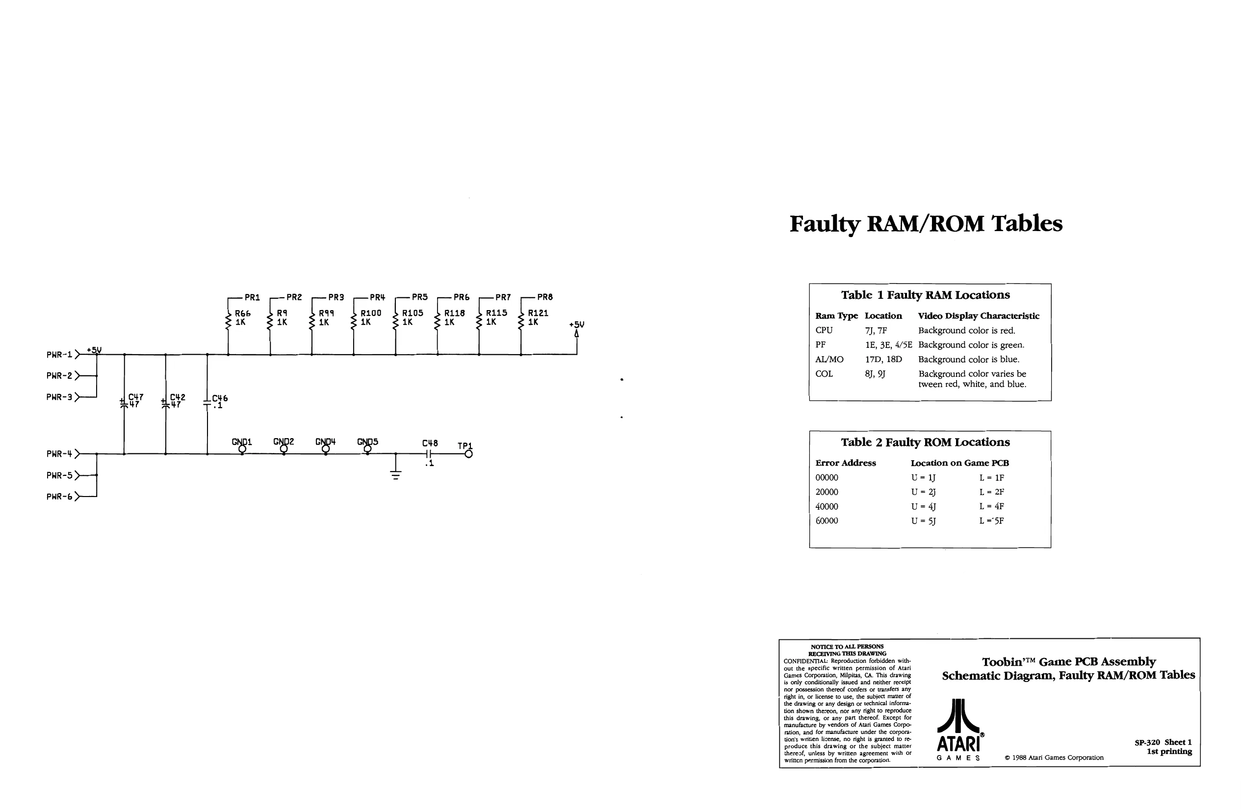
Faulty RAM/ROM Tables
PRZ PRB PRY PRS PR6 PRT PRE Table 1 Faulty RAM Locations
Ra Ra9 rico $rios brits Sriis ria ak 1k ik 1k 1K 1K ik a Ram Type Location Video Display Characteristic cPU J, 7E Background color is red. PF 1E, 3E, 4/SE Background color is green. AL/MO 17D, 18D __ Background color is blue. . COL 8), 9 Background color varies be tween red, white, and blue.
id og 5 cus me Table 2 Faulty ROM Locations
f A Error Address Location on Game PCB
| PHR-5 | = | 00000 | u-y | L=1F |
| PHR-& | 20000 | uU=3j | L=2F | |
| 40000 | u=4 | L=4F | ||
| 60000 | u=3 | L=SF |
NOTICE TO ALL PERSONS
G THIS DRAWING
RECEIVING
CONFIDENTIAL: Reproduction forbidden with- Toobin’™ Game PCB Assembly
‘out the specific written permission of Atari E uli /ROM Tr bl Games Corporation, Milpitas, CA. This drawing Sch ‘ables i only ondtionaly sued and nether rect ematic Diagram, Faulty RAM. noe possession thereof confer or traraers any fightin, or license to ut, the subject mater of the drawing or any design or technical information shown thereon, nor any right to reproduce this drawing, or any part thereof. Except for manufacture by vendors of Atari Games Corporation, and for manufacture under the corpora- ® fom wmten lene, no night & grmed re weeduce his dnwing onthe seoee mater = ATARI SP-320 Sheet 1
ereof, we with Ast printing
‘area peels ben ta-seeanen “ GAMES © 1988 Atari Games Corporation Pp
This page is a drawing, shown as the original scan.
This page is a drawing, shown as the original scan.
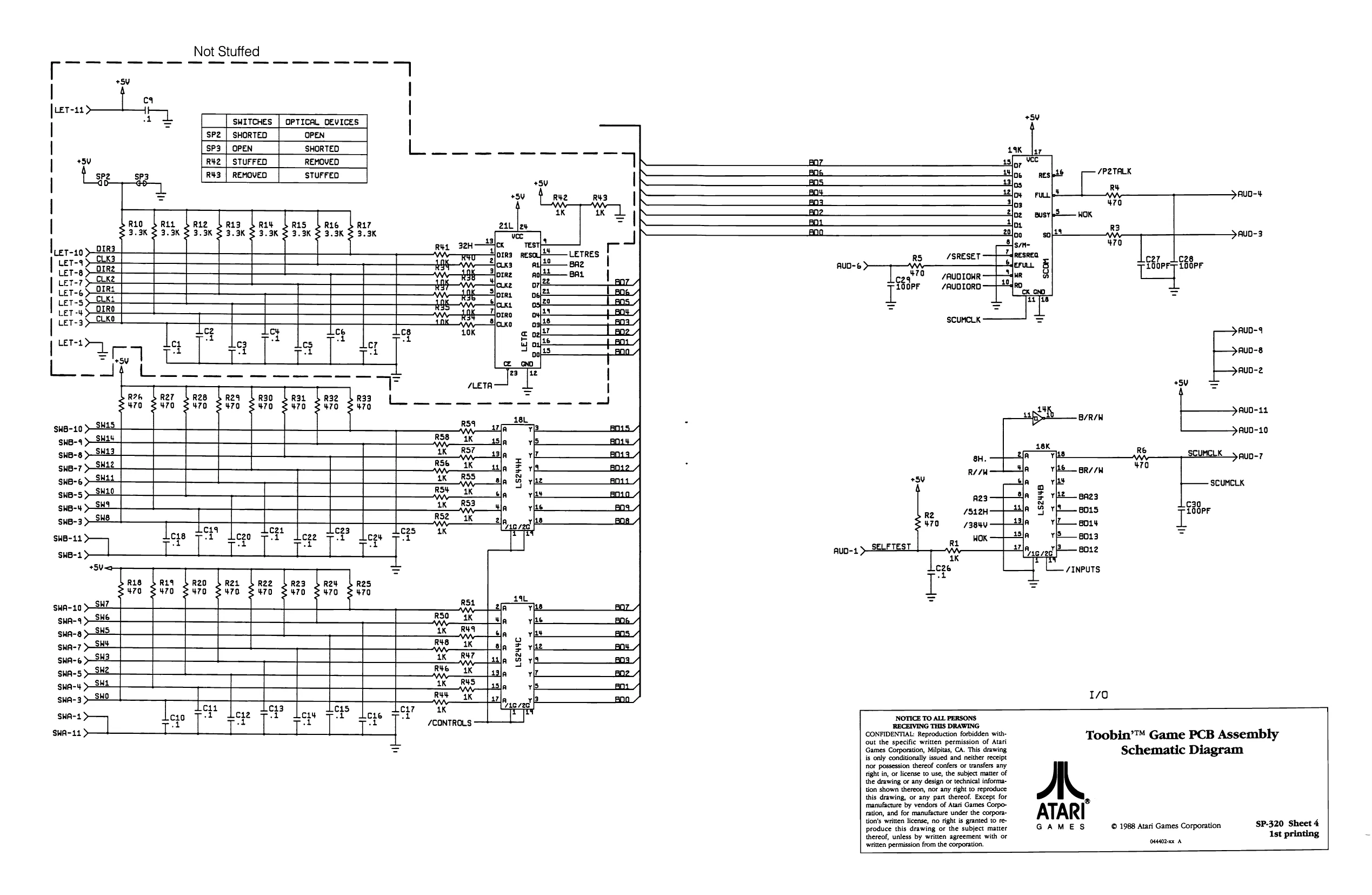
This page is a drawing, shown as the original scan.
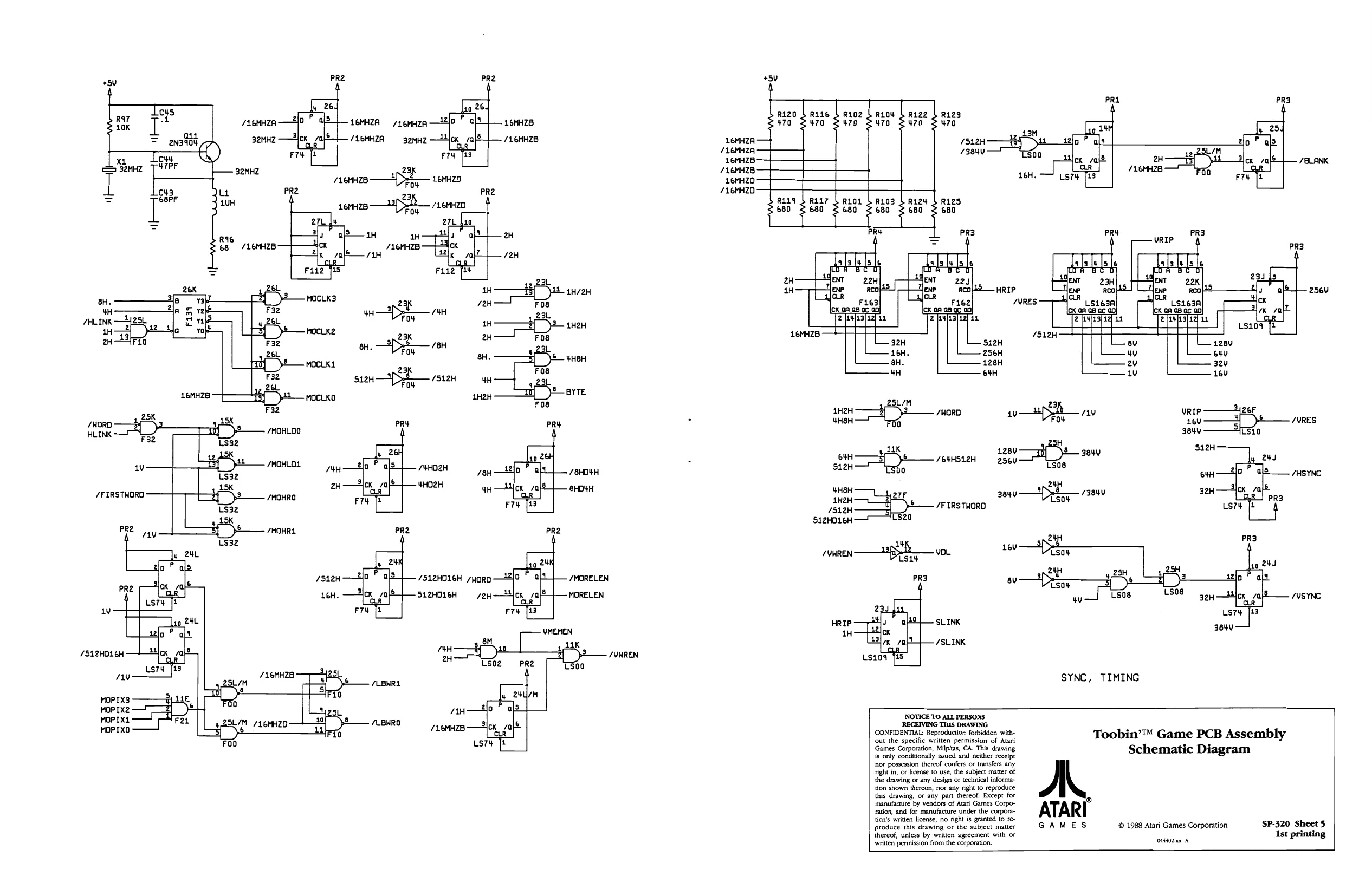
This page is a drawing, shown as the original scan.
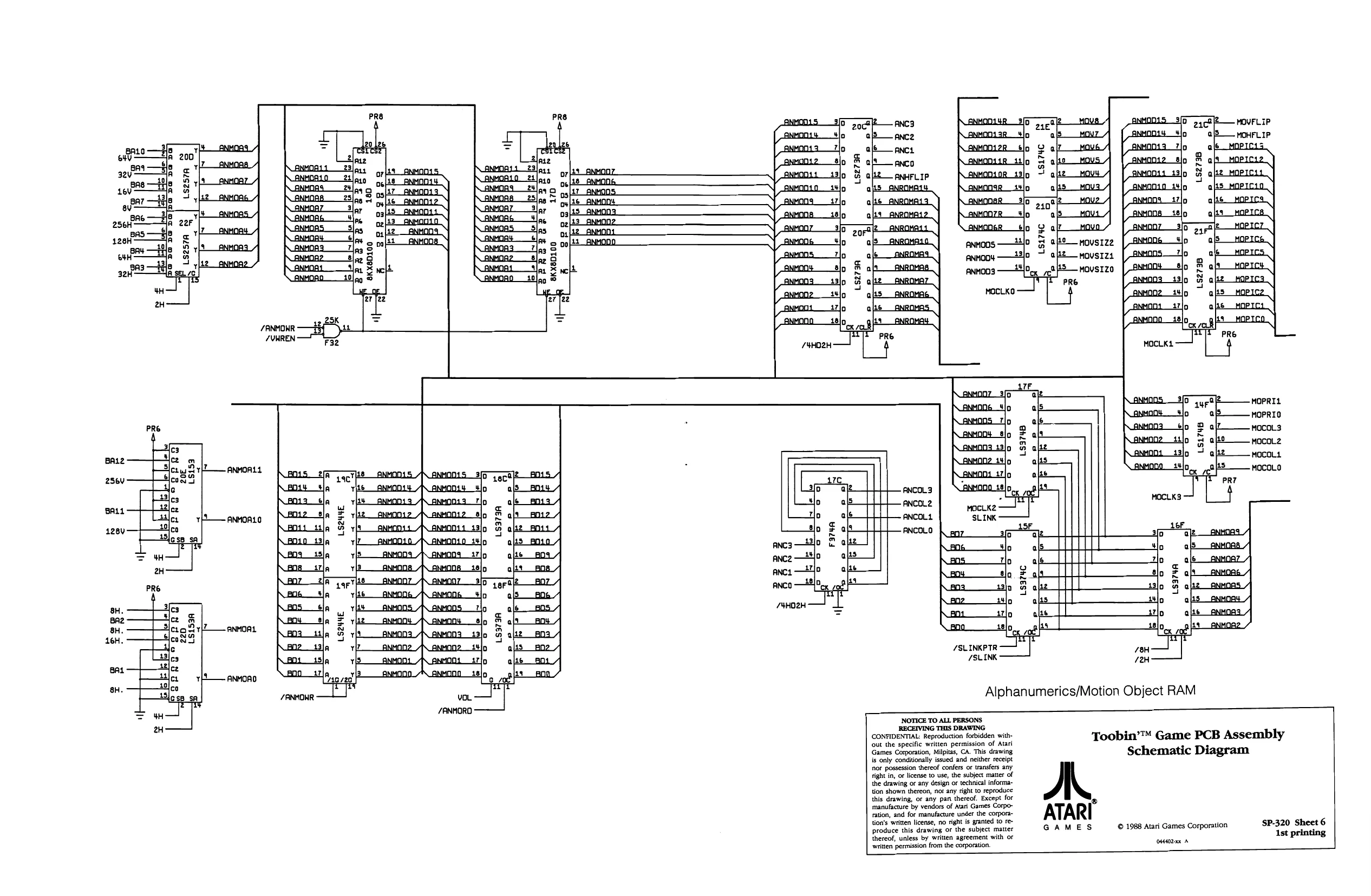
This page is a drawing, shown as the original scan.
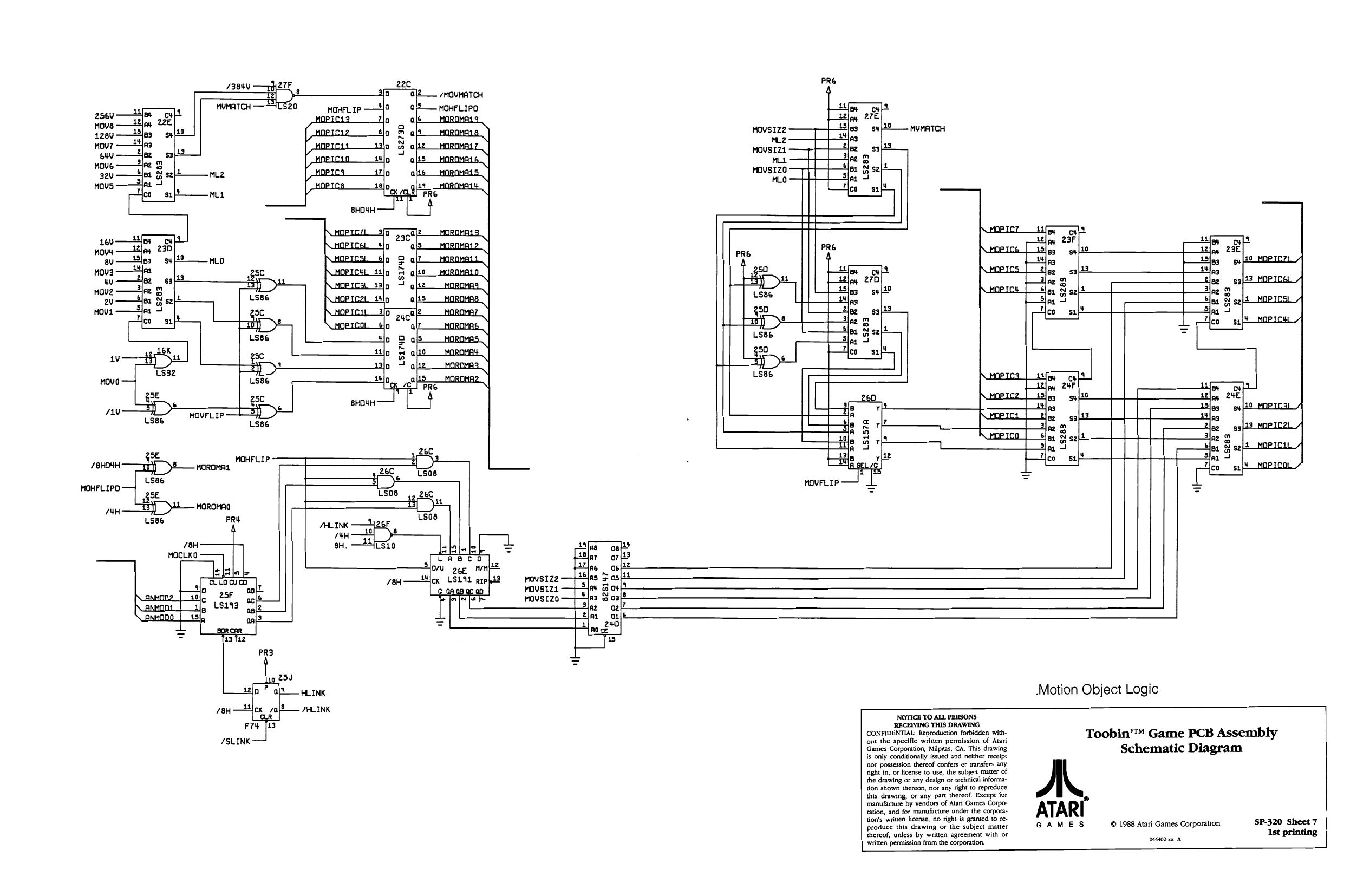
This page is a drawing, shown as the original scan.
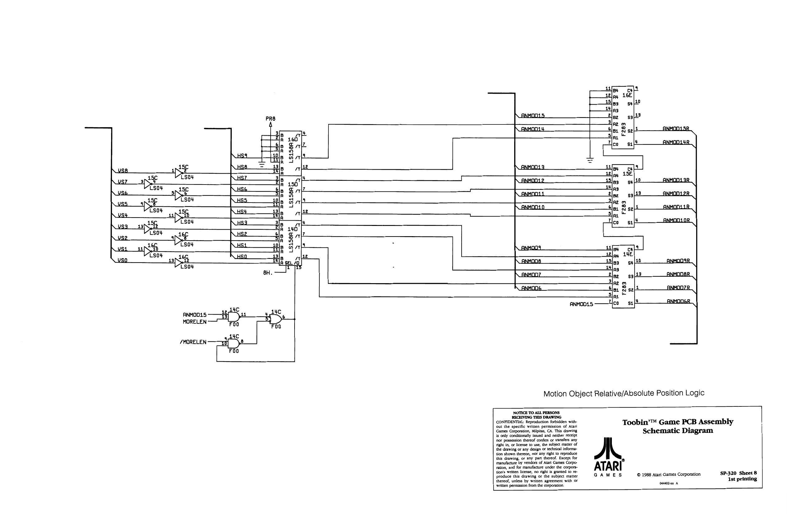
This page is a drawing, shown as the original scan.
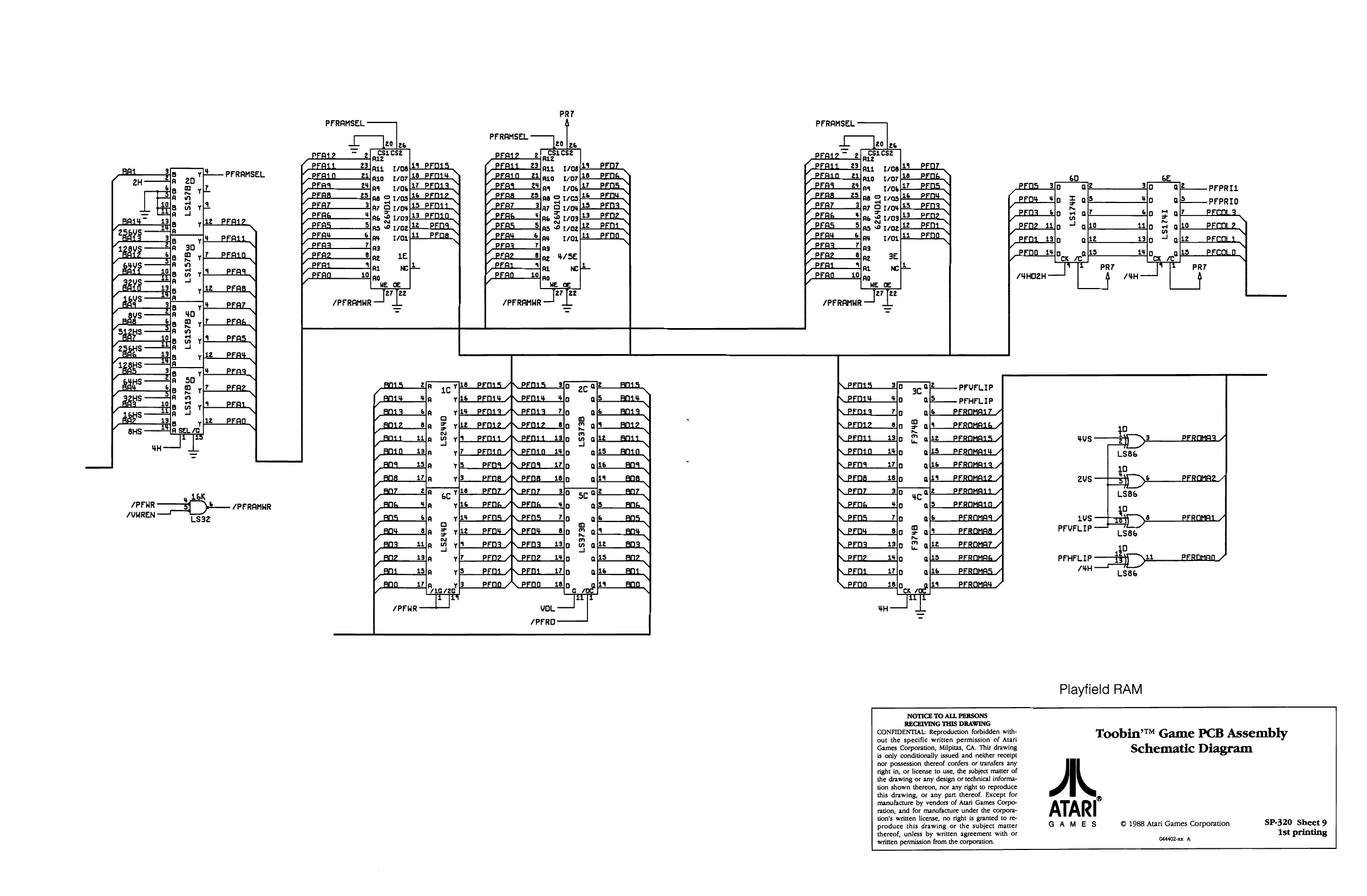
This page is a drawing, shown as the original scan.
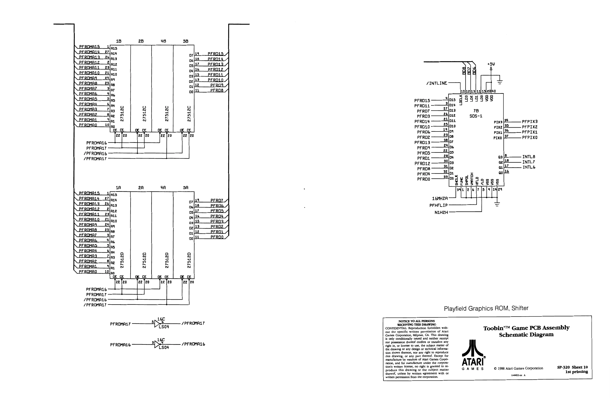
This page is a drawing, shown as the original scan.
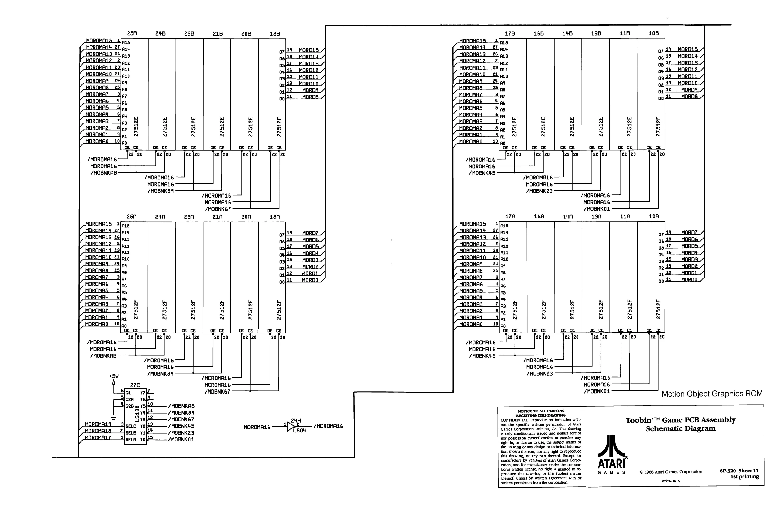
This page is a drawing, shown as the original scan.
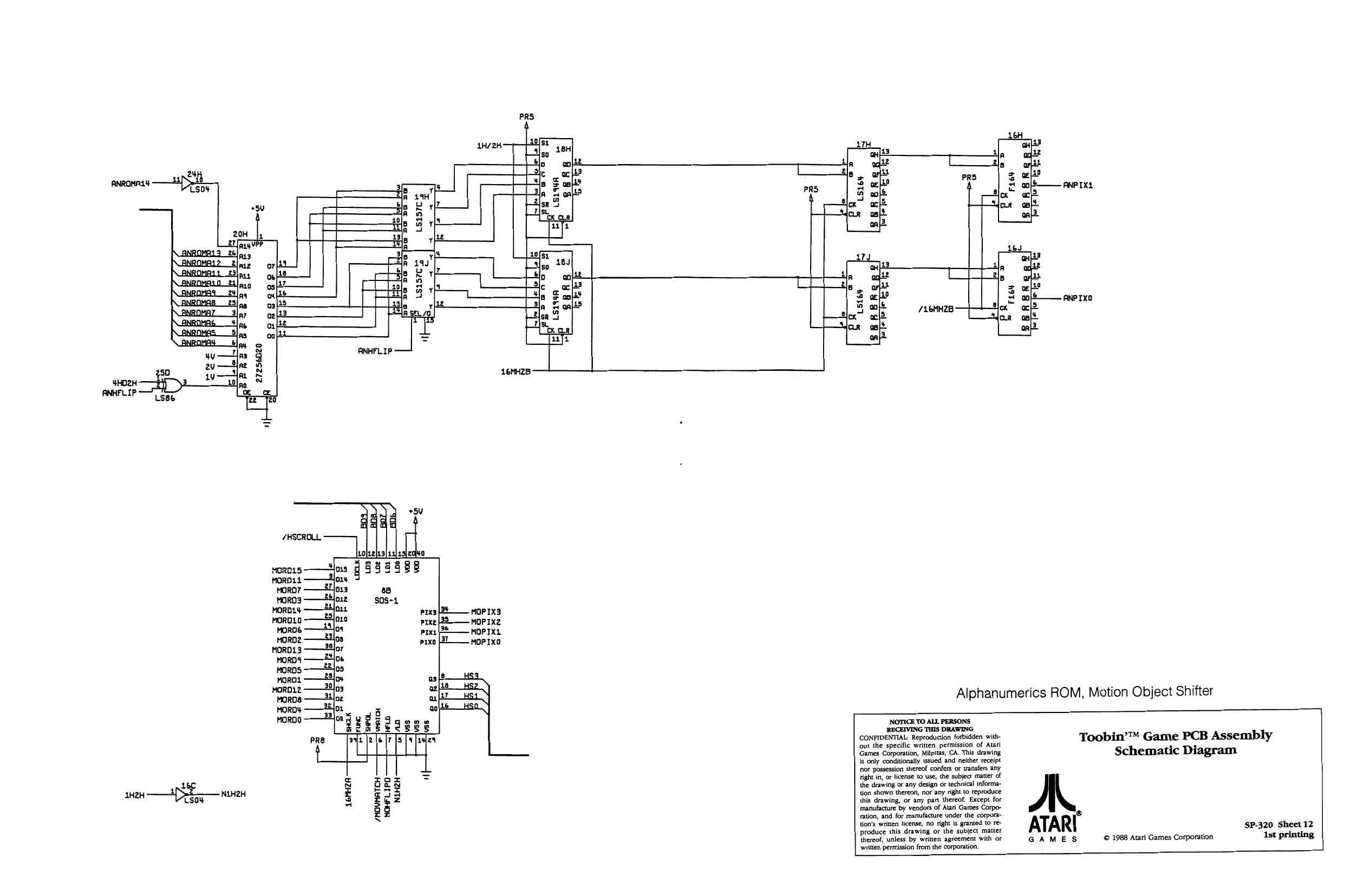
This page is a drawing, shown as the original scan.
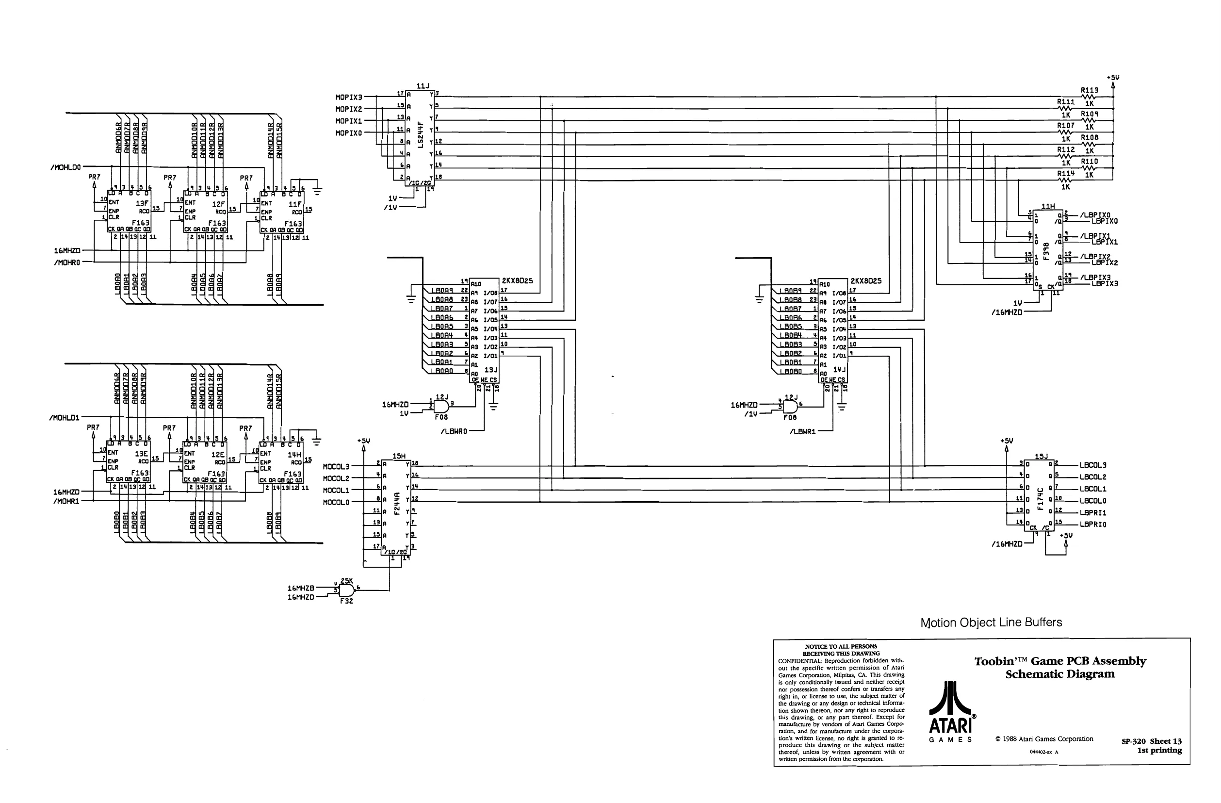
This page is a drawing, shown as the original scan.
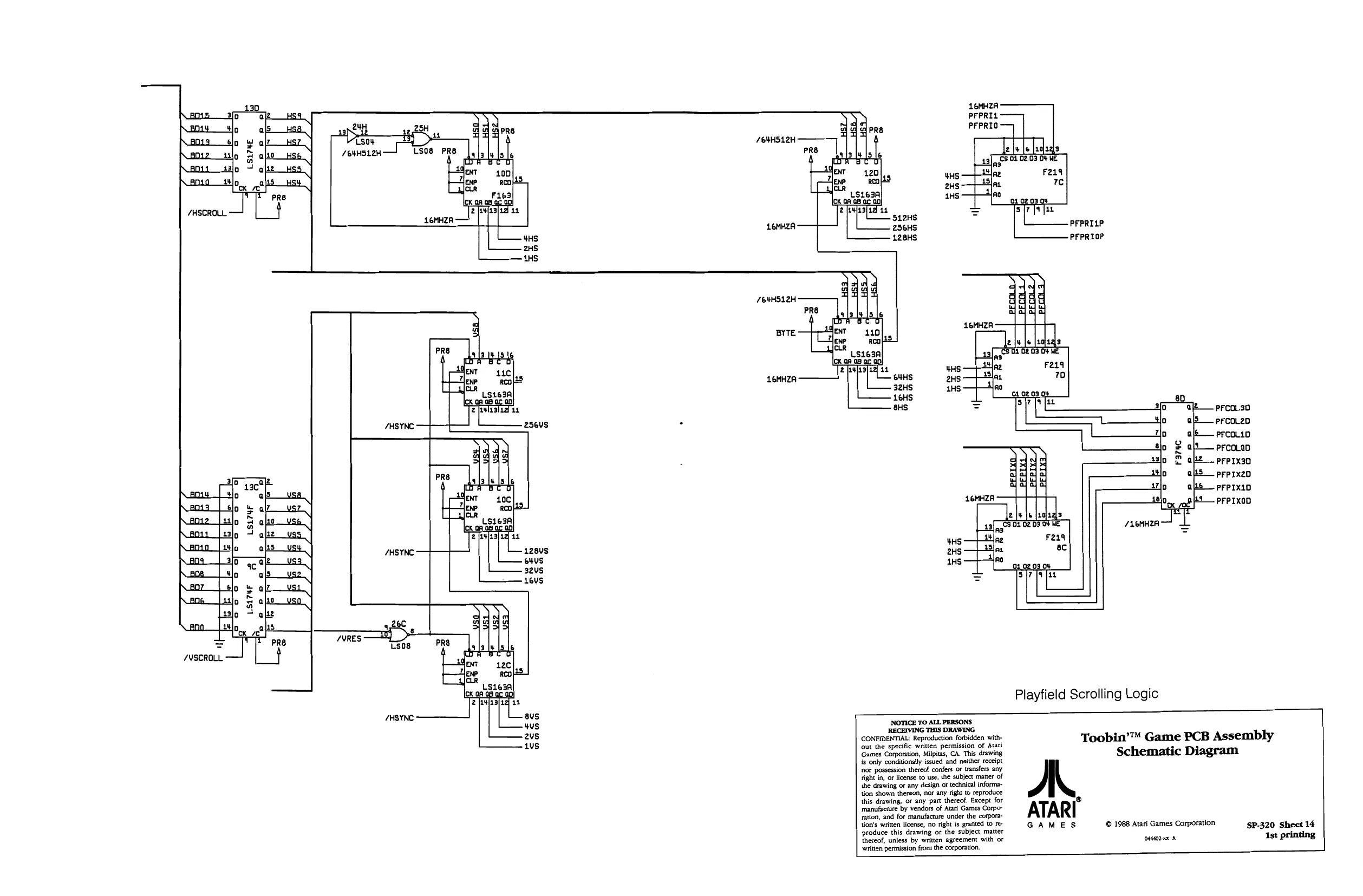
This page is a drawing, shown as the original scan.
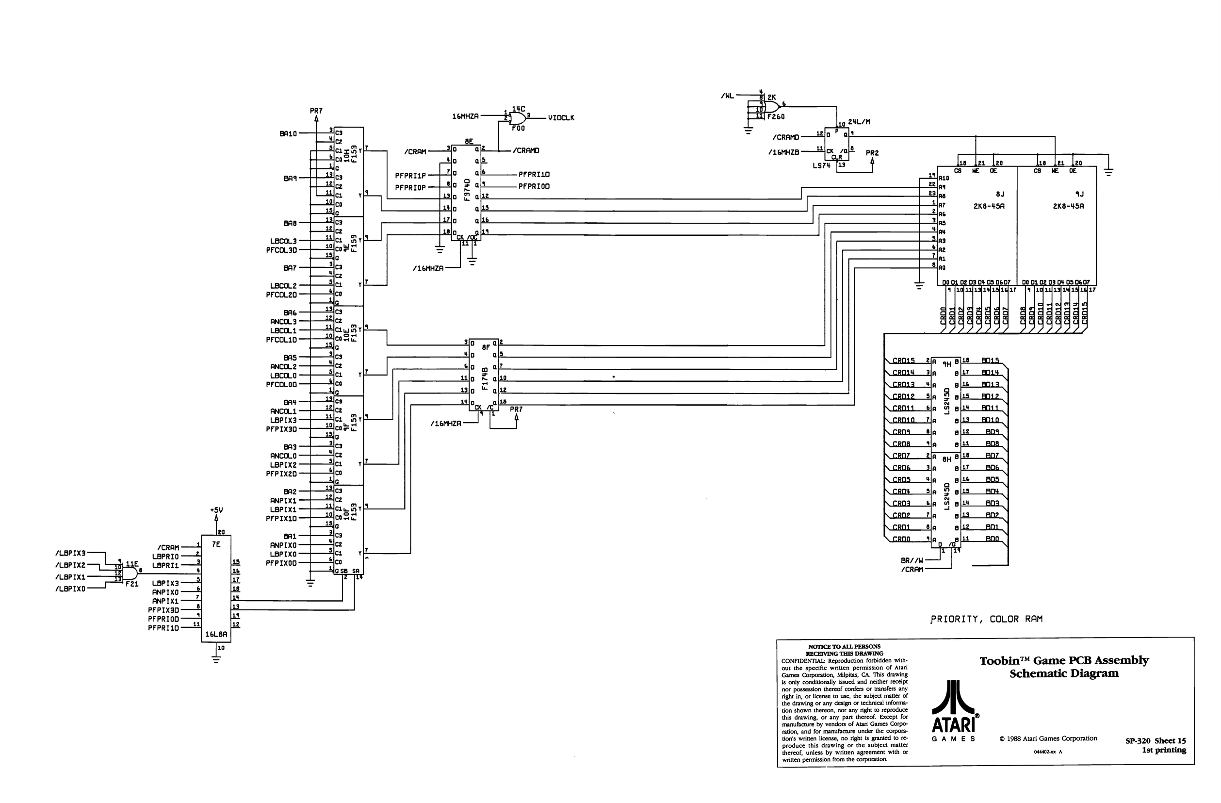
/LBPIX3:
/LBPIX2
/LBPIXL
/LEPIXO atte LGMHZA 2 vrei
PFPRILO
PFPRIOD aL 2K
F260
Tso [es [es Tl cS ME OE lato As ae 8d or) 2K8-45A
PFCOL1D
BAS ANCOL2 LBCOLO PFCOLOD
BAY — ANCOL1 LBPIX3 PFPIX3D
BAZ ANCOLO —y LBPIX2 PFPIX20
BAZ ANPIXL LBPIX4 PFPIX10
BAL ANPIXO. LBPIXO PFPIXOD F174B
PRT
PRIORITY, COLOR RAM
CONFIDENTIAL: Reproduction forbidden without the specific written permission of Atari ‘Games Corporation, Milpitas, CA. This drawing is only conditionally issued and neither receipt nor possession thereof confers or transfers any
right in, of license to use, the subject matter of ‘manufacture by vendors of Atari Games Corpo ton's ‘written license, no right is granted to re
the drawing or any design or technical information shown thereon, nor any right to reproduce this drawing, or any part thereof. Except for ‘manufacture by vendors of Atari Games Corporation, and for manufacture under the corporaton's ‘written license, no right is granted to reproduce this drawing or the subject matter thereof, unless by written agreement with or ‘writen ‘permission from the corporation,
Toobin™ Game PCB Assembly
Schematic Diagram
‘s
ATARI
GAMES © 1988 Atari Games Corporation SP-320 Sheet 15 oMdon-ex A 1st printing
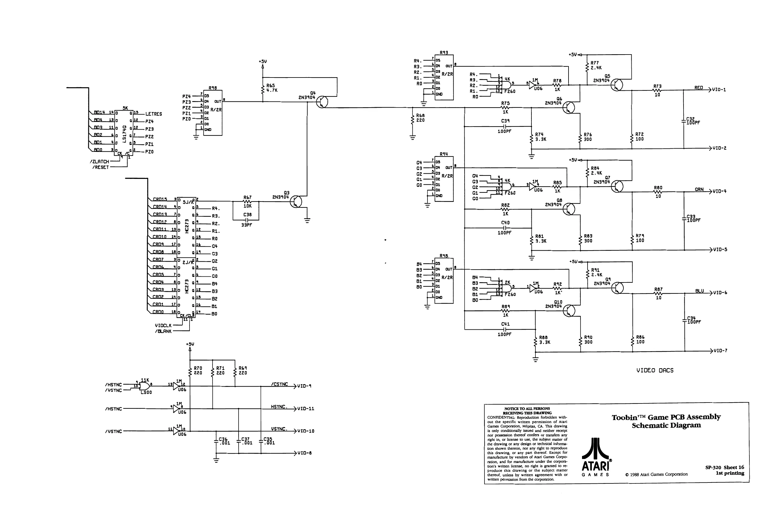
This page is a drawing, shown as the original scan.
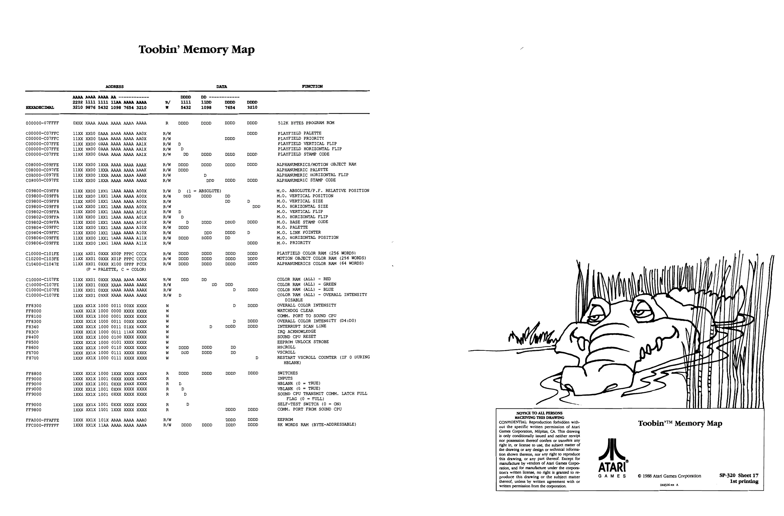
This page is a drawing, shown as the original scan.
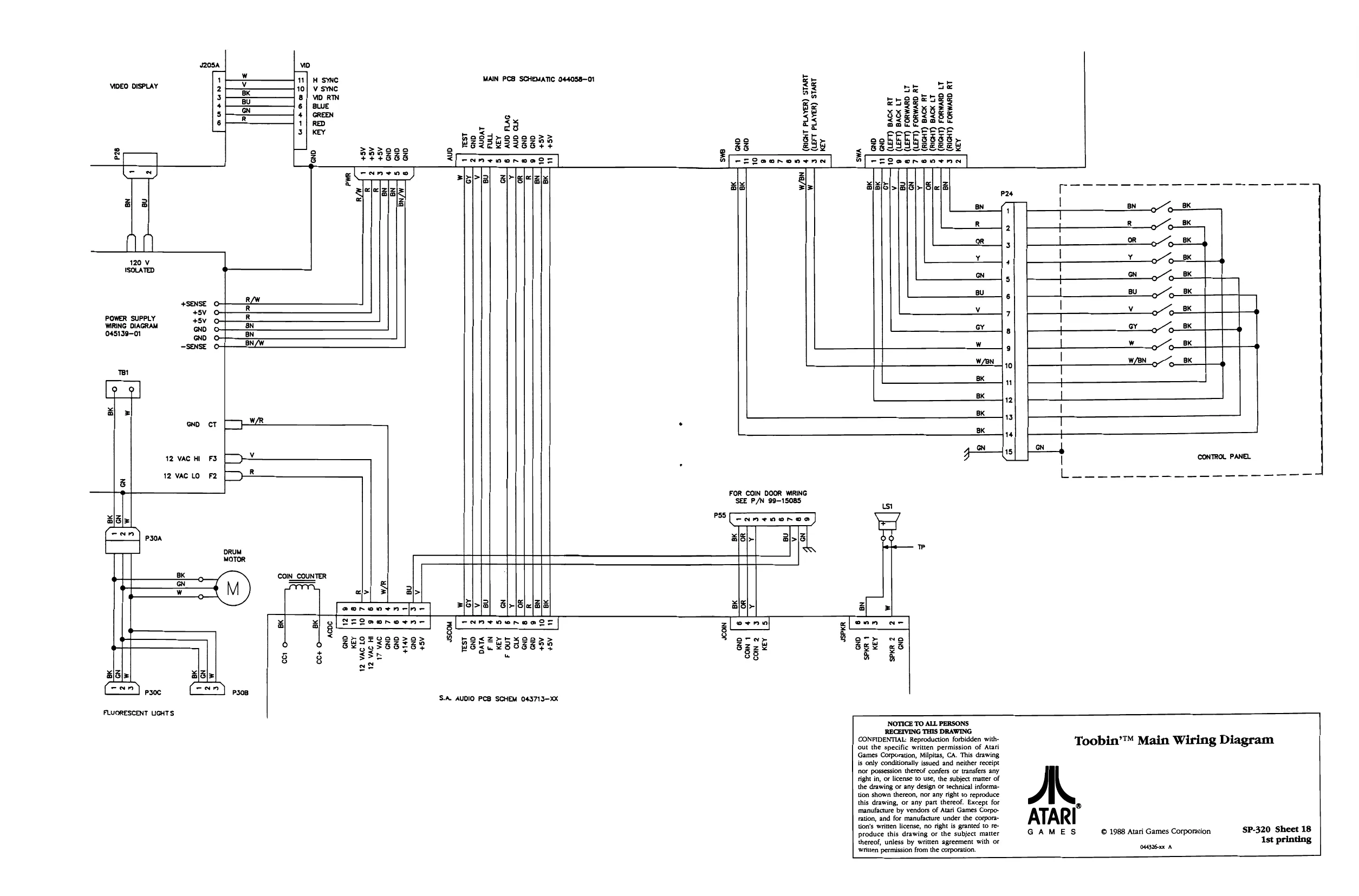
This page is a drawing, shown as the original scan.
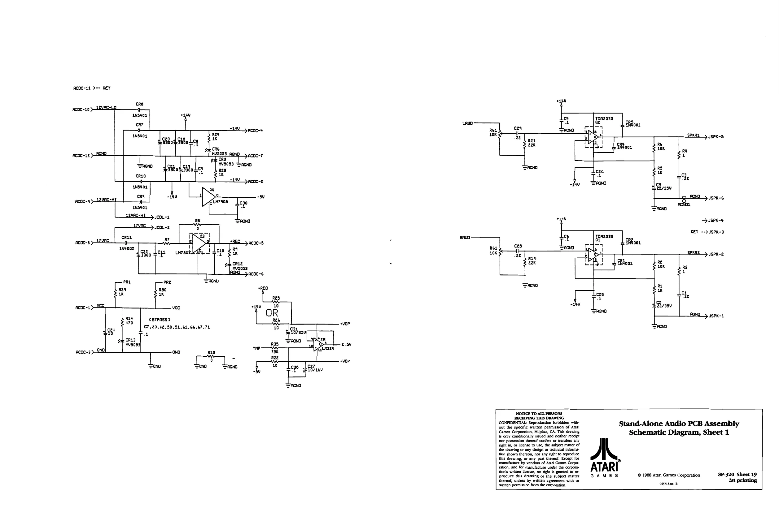
ACDC-11 >-- KEY
pcoc-10
Acoc-12
Acoc-8
PRL PRE ACN
vec
cBYPASS)
C7,23,42,50,51,61,66,67,71
a
NOTICE TO ALL PERSONS
RECEIVING THIS DRAWING CONFIDENTIAL: Reproduction forbidden without the specific written permission of Atari Games Corporation, Milpitas, CA. This drawing. {s only conditionally issued and neither receipt ‘nor possession thereof confers or transfers any
right in, or license to use, the subject matter of tion shown thereon, nor any right to reproduce ‘manufacture by vendors of Atari Games Corpo tion's ‘writen license, no right is granted to re
the drawing or any design or technical inform
this drawing, or any part thereof. Except for
ration, and for manufacture under the corpora tion's ‘writen license, no right is granted to reproduce this drawing or the subject matter thereof, unless by written agreement with or ‘written permission from the corporation. AL JSPK-S
JSPK-6
> ssPK-4
KEY -->JSPK-3
ISPK-2
JSPK-1
Stand-Alone Audio PCB Assembly Schematic Diagram, Sheet 1
ATARI GAMES
‘© 1988 Atari Games Corporation ‘SP-320 Sheet 19 (043713-xx B 1st printing
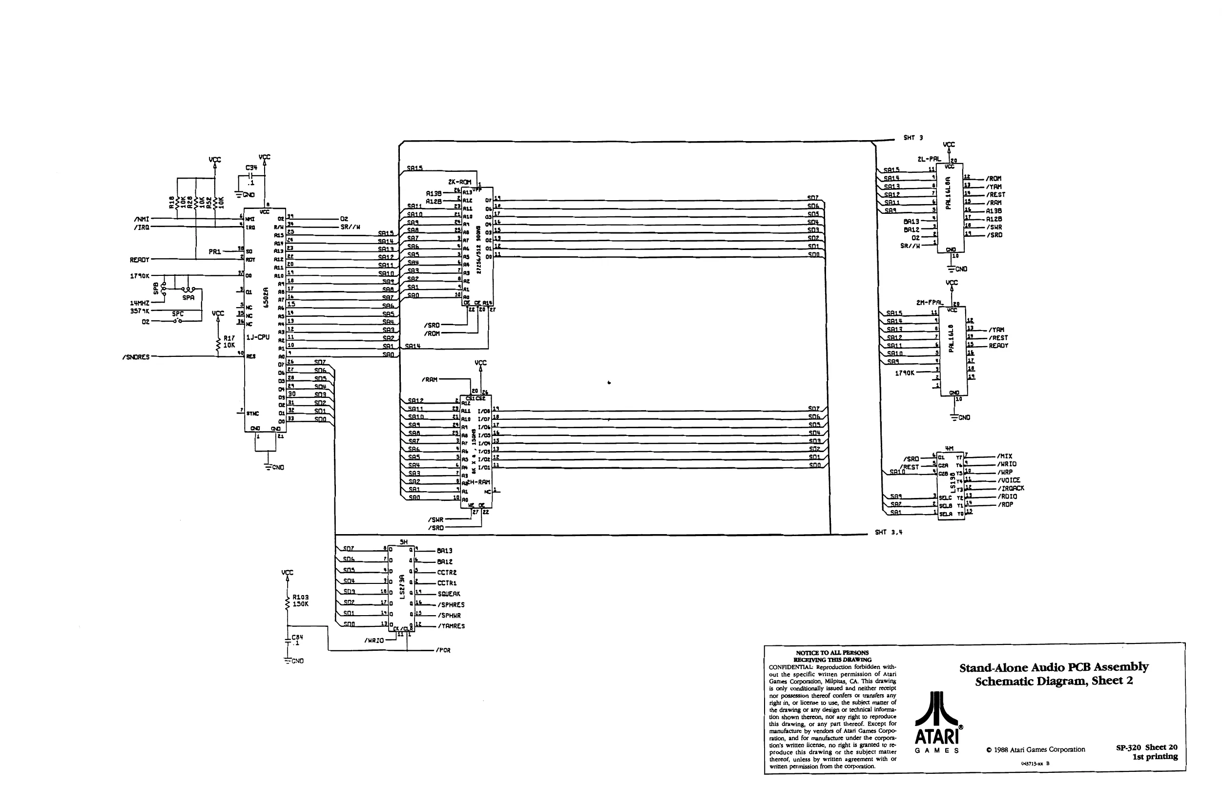
This page is a drawing, shown as the original scan.
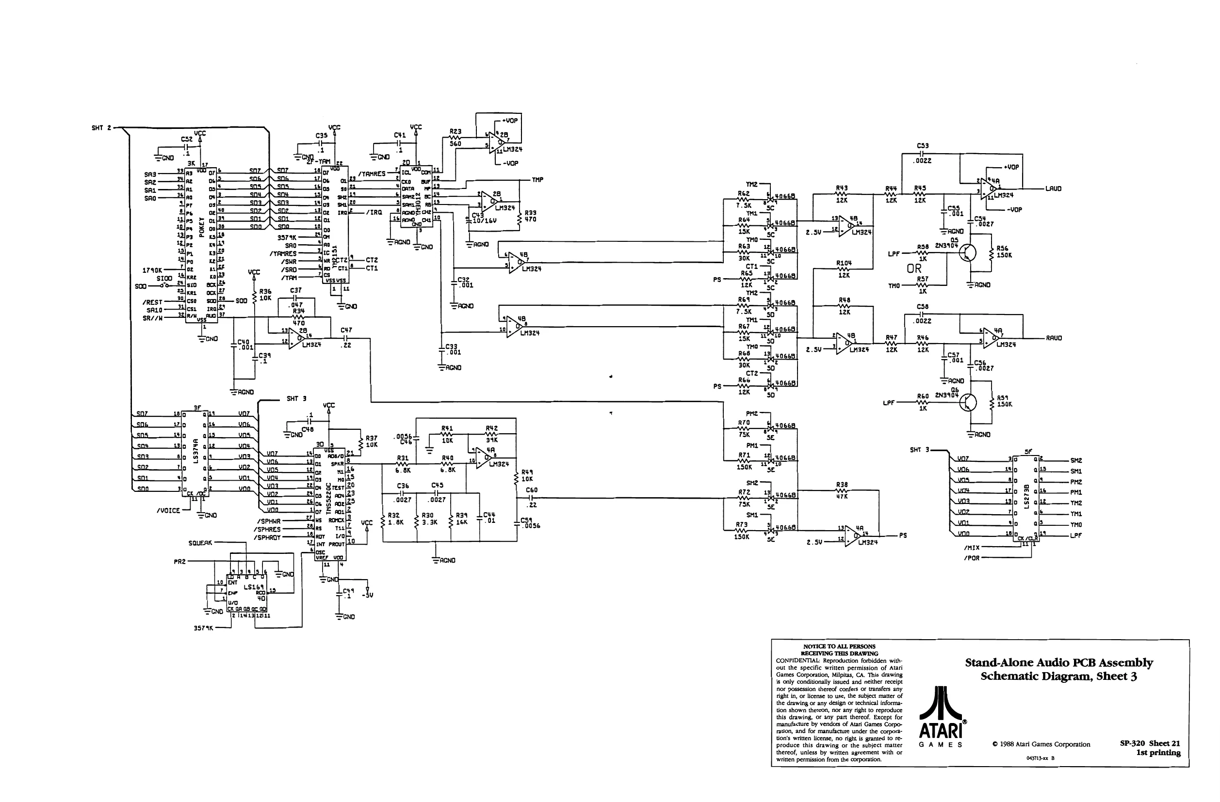
This page is a drawing, shown as the original scan.
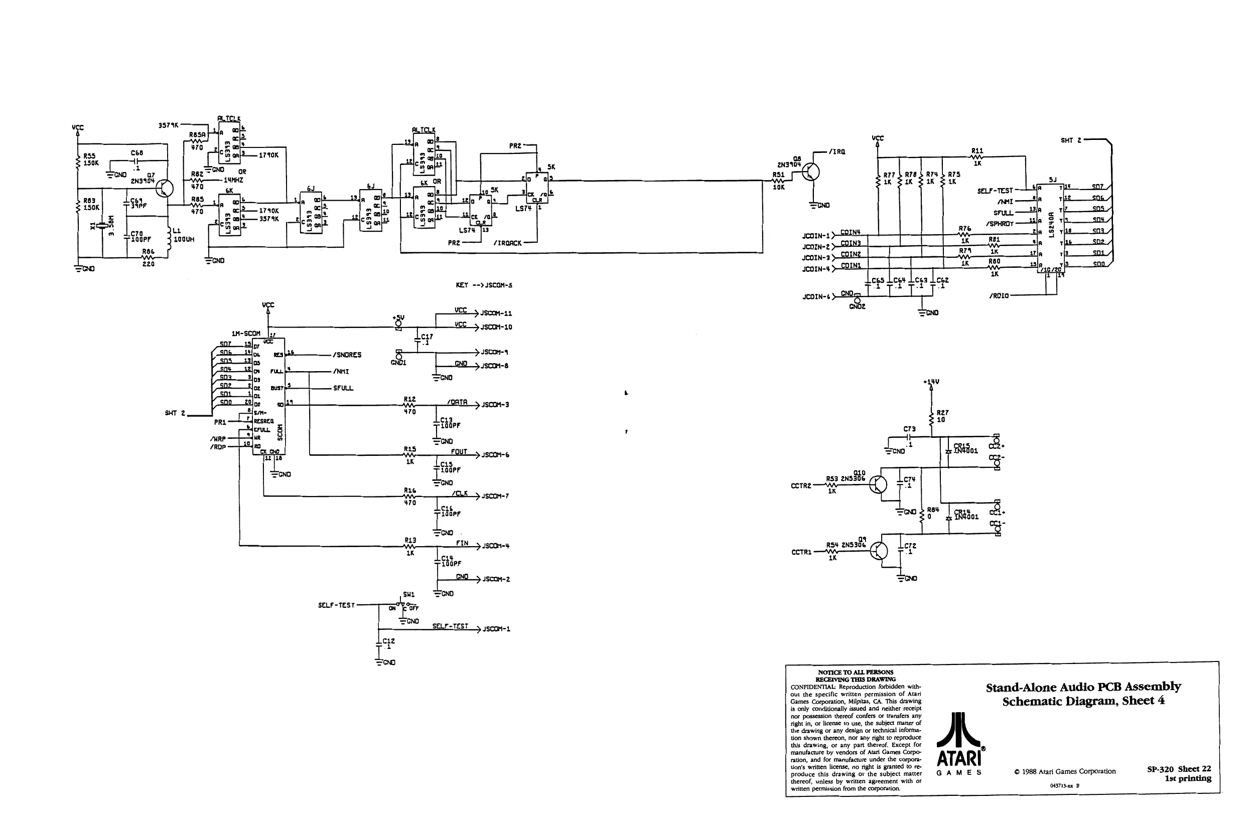
This page is a drawing, shown as the original scan.
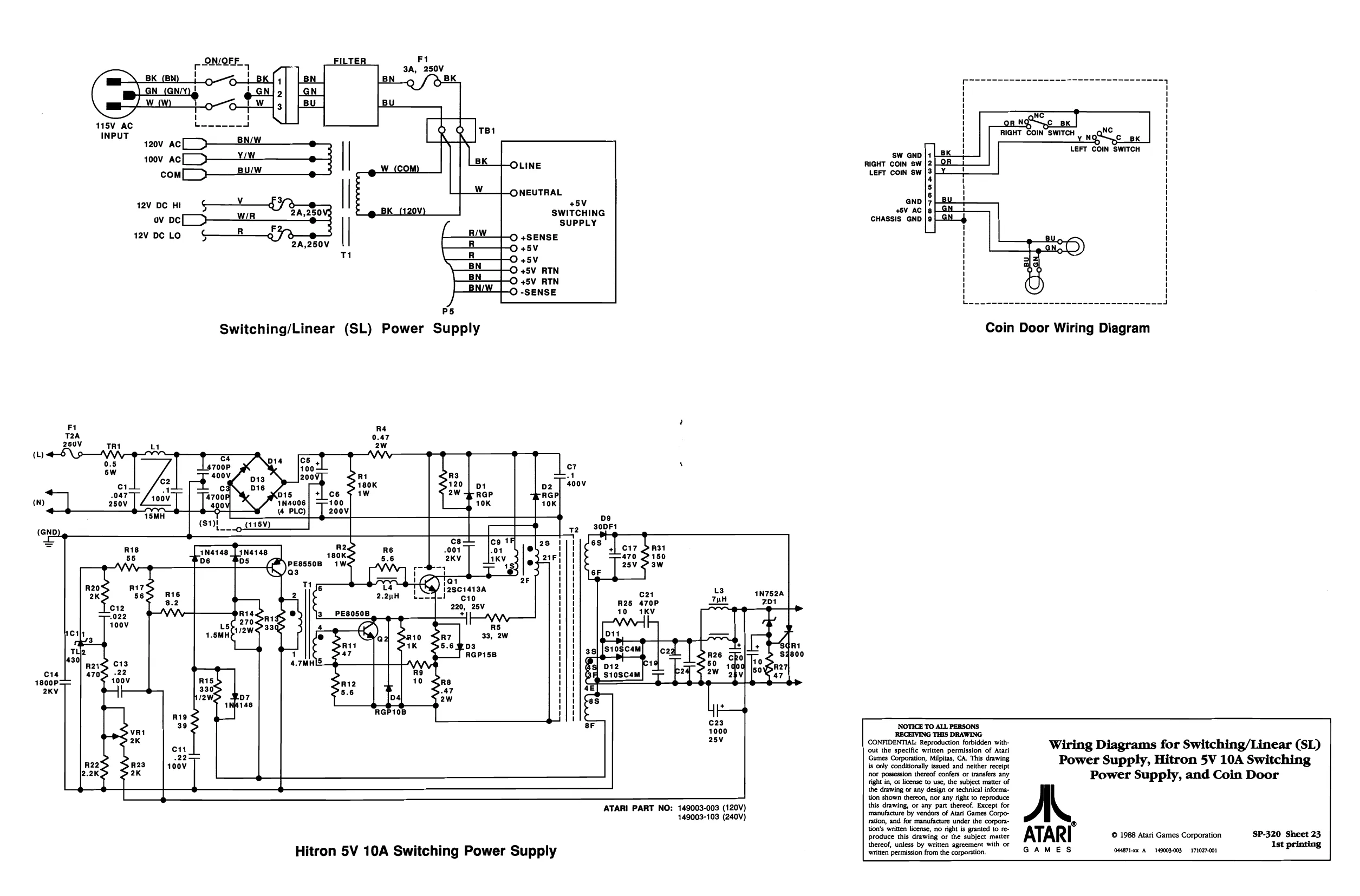
INPUT N cB H i
H
W5V AC 2 been nn: H i 1 bo} | LEFT COIN SWITCI 120V AC SW GND 100V AC RIGHT COIN SW com[__——2u/w LEFT COIN SW
ONEUTRAL @nd 45 AC CHASSIS GND +5V SWITCHING SUPPLY 12V DC HI
ov pc|
12V DC LO we taHasons 2A,250'
F z +SENSE
+5V +5V +5V RTN +5V RTN -SENSE 2A,250V | v1
Switching/Linear (SL) Power Supply Coin Door Wiring Diagram
SC1413A c10 220, 25V +
RS 33, 2W D3 RGPISB
CONFIDENTIAL: Reproduction forbidden with- Wiring Diagrams for Switching/Linear (SL) out the specific written permission of Atari Games Cor 1, Milpitas, ‘This drawi Bae opooin, tonas Ch The craving Power Supply, Hitron 5V 10A Switching
for postession thereof confers or transfers any Power Supply, and Coin Door
right in, or license to use, the subject matter of
the drawing or any design or technical information shown thereon, nor any right to reproduce ATARI PART NO: 149003-003 (120V) this drawing, or any part thereof. Except for : manufacture by vendors of Atari Games Corpo- 149003-103 (240V) ration, and for manufacnure under the corpora ; i per 7 proce te ‘awng oF te sea ATARI © 1988 Atari Games Corporation sP320 Sheet 23 . thereof, unless by waiten agreement With oF print Hitron 5V 10A Switching Power Supply writen permission Bom the corporation. GAMES arian A ven03403 cara