Star Trek Deluxe Game Kit Owners Manual (420-1023)
Star Trek (Sega, 1982) · Owner's Manual · 142 pages · 57 sections · original scan
STAR TREK.
SEGA
Deluxe Game Kit Owner’s Manual
Manual Part No. 420-1023
Cy
c=
on
Deluxe Game Kit
Owner's Manual
Manufactured By
TLX 910-335-1621
STAR TREK™ Owner's Manual Copyright © 1983 by SEGA Electronics, Inc., All Rights Reserved STAR TREK™ Indicates a Trademark of Paramount Pictures, Inc.
1? v4 a]
Co
Ez.
i Table of Contents
List of Illustrations Introduction... ee ee ee eee a Game Set Up & Inspection...) eee ee ee es
Table of-Contents (Cont.)
Universal Sound Board Assembly ......... eee eee. 102 Speech Board’ Assembly ... 2... -. 0.2.2 eee ee oe eo - 105 G-80 Power Supply Assembly -.........4- Leek ee. 109 G-80 Power Supply PC Assembly .. 2... 2... eee eee 113 Schematics ; ;
Comments Mailer ”
Goo
{ oo
Cz, C2,
C2
C, List of Illustrations
G-80 Bus Detail 2. 1 1 1 ee ee ee ee ee ee 15 G-80 Mother Board Bus Pin Assignments .... 2... 2.2 e ee eee 16 G08-003 Color X-Y Monitor Block Diagram... ....- +22 eee 39 G08-003 Color X-Y Monitor Illustrations ..... 2... eee eee 50 AC Junction Box Assembly . 2... 6. 1 ee eee ee ee ee ee 60 EMI Transformer Assembly .. 2... 22 2s eee ee eee eee 62 Single Player Control Panel Interface Assembly .......... 64 Rotary Control Interface Assemlby ......-....-2.5002008 66 , Rotary Control Assembly ......... eee eww ee ee wee 68 Monitor Power Harness Assembly .........-2.-2-222220.8 69 Speaker Harness Assembly .. 21... 1.0 e ee eee ee eee 70 Power Harness Assembly .. 2... 2. eee ee eee ee ee ee 71 Control Panel Interface Harness Assembly ............. 72 Video Harness Assembly . 2... 2.2.2. ee ee eee eee eee 73 Control Panel Harness Assembly ..........0202050008 74 G08-003 Color X-Y Monitor Assembly .............20- 81 44-Pin Extension Board 2... 1... ee ee 83 Game Electronics Assembly... .......0.2.-.0 200 eee 85 G-80 Universal Cage Assembly .........2.0222.00008. 87 CPU Board Assembly ... 2... 2... ee ee ee ee 91 EPROM Board Assembly ..........2.2..0000 000 eee 94 X-Y Timing Board Assembly... 1... ee ee ee ee ee 97 X-Y Control Board Assembly . 2.2... ......02.0.000. 100 Universal Sound Board Assembly ...............20.4 104 Speech Board Assembly... 2... ee eee ee ee 108 Power Supply Assembly... ........0..-2.2.000200008 112 Power Supply PC Assembly ...........0200 000 eee 115 Schematics 44-Pin Extension Board... 2... 2 2. ee ee ee 116 Cabinet Wiring Diagram. 2... . 2. ee eee ee 117 EMI Transformer AC Junction Box Game Electronics... 2... ee ee ee 118 Single Player Control Panel Interface ........... 119 CPU Board 2. fe ey 120 EPROM Board 2... . . eee ee ee ee 122
List of Illustrations (Cont.)
X-Y Timing Board 2 2. ee 123 X-Y Control Board 2... ee eee eee 126 Universal Sound Board . 2... ee ee eee 128 Speech Board. 2.2... ee ee eee 131 oe ees eens
<3
ae es es es ed as
(2 fo fs te
Cc
C
(=
Cy
on Introduction
STAR Trex™ is a microprocessor based coin-operated electronic game, that makes extensive use of digital integrated circuitry and television monitor concepts. This manual is designed for the use of the maintenance technicians who possess a general working knowledge of solid-state circuitry and video monitor theory. Any individual NOT knowledgeable in these areas SHOULD NOT attempt repair of the electronic portions of the game. In addition to this manual and training in electronics, troubleshooting and repair will be facilitated by: access to general electronic-type handtools, a multimeter, a 50 to 100 MHz oscilloscope and a logic probe would be helpful. Technical assistance is available toll-free by calling: 1-800-854-1938 outside California 1-800-722-8576 inside California Parts information assistance is available toll-free by calling: 1-800-854-1900 outside California 1-800-722-8575 inside California
i or any of our games are Questions or comments concerning STAR TREK welcome and should be directed to: Customer Service Manager SEGA Electronics, Inc. 16250 Technology Drive San Diego, California 92127-1985
Game Kit Set Up & Inspection
INSPECTION Upon receipt of your new STAR TREK Deluxe Kit, be sure to verify its contents against the enclosed parts list to ensure its completeness. Inspect the Color X-Y Monitor closely for damage, as well as the electronic components of the kit, and either notify your distributor of any discrepencies in the kit, or the shipping company involved of any damages as soon as possible. Check to ensure that the four Power Supply PC Board (P/N 800-0170) fuses are intact, in addition to your existing cabinet's AC Input fuse(s), and the four fuses located on the Main PCB of the Color X-Y Monitor (P/N 200-0025).
VOLTAGE SELECTION
Upon completion of your kit's installation, and before plugging in your new game, make sure that the game voltage is correct for your location. Identify the two leads from the AC Input to the EMI Transformer Assembly (P/N 800-0190). For 110 VAC they should be connected to terminals 1 and 3 on the power transformer. For 100 VAC, connect 1 and 2, and for 220 VAC applications, they should be connected to terminals 1 and 4.
POWER REQUIREMENTS
100 VAC, 60 Hz (nominal), 1 9, 150 watts 110 VAC, 60 Hz (nominal), 1 9, 150 watts 220 VAC, 60 Hz (nominal), 1 9, 150 watts
INSTALLATION
Begin by assessing your particular video game with regard to those components of the game which are to be replaced (i.e. monitor, power supply, electronics, graphics, etc.). Items from your old cabinet that will be fetained are, 1) control panel, 2) coin mechs, 3) coin counter, 4) service and reset switches (if any), and 5) speaker (8 ohm). Monitor replacement can be done first and is certainly the most delicate (if not cumbersome) operation involved. Extreme care should be excercised in handling both monitors. The Color X-Y Monitor will be installed horizontally and as a consequence may require you to rotate your existing monitor bracket
90°. Installation of the electronics is a simple matter of physically securing the Game Electronics (P/N 800-3305) and G-80 Power Supply (P/N 800-0191) into the cabinet interior, and referring to the Cabinet Wiring Diagram to -)
oe oes oe: ios is ees oes Ens
INSTALLATION (cont.)
interconnect the component Assemblies. Open-ended harnesses are provided for the interfacing of, a) the Rotary Control Interface Board (P/N 800-0374) and the 44-pin Extension Board (P/N 170-0281), and b) Video data and the Extension Board. The 44-pin Extension Board is used as a "Master-interconnect" for nearly all Input/Output ports. The Extension Board is plugged into the G-80 card cage cover, and individual wires are soldered directly to the terminal pads (as detailed both on the Cabinet Wiring Diagram [Drawing No. 700-0140], and the 44-pin Extension Board assembly illustration). "All-up" harnessing is provided for EMI Transformer and Power Supply connections both for Game Electronics and monitor display requirements, in addition to a speaker harness for audio input to any 8 ohm speaker. Volume Control is accomplished by way of a 10K ohm potentiometer wired to the Extension Board as seen in the Cabinet Wiring Diagram.
Important Notes
The following note is included in compliance with FCC rules:
Operation of this equipment in a residential area is likely to cause interference in which case the user ar his own expense will be required to take whatever measures may be required to correct the interference.
Additionally:
NEVER remove circuit board connections while power is on.
NEVER replace any components with anything other than exact replacement parts.
NEVER replace fuses with anything other than the proper value. A blown fuse indicates an overload condition within the game. Replacing the fuse with a higher value can cause serious damage to internal components. ps es ee |
J aaa Sp
=
a)
ly Cc
C2.
C2
ion
Cz
t
Game Concept
STAR TreK™ is a one or two player SEGA Color X-Y video game with computerized speech synthesis. The player finds himself the Captain of the Starship Enterprise, his mission being to rid the universe of a number of threats to the United Federation of Planets.
STAR TREK™ has a unique method of displaying the information vital to the
game play. This method involves the separation of the CRT into three , completely separate "screens".
Status Scanner u —~. —_—
The "Scanner" is where the player sees a "top down" or plan view of local space, with the Enterprise always in the center of this screen. The "Viewer" is where the player sees actual “apparent 3-D" images, as if he were looking out the ships front window. The "Status" screen displays player score in addition to Shield strength, number of Photon Torpedoes, and amount of Warp energy remaining.
The game begins by introducing Klingons, Starbases and the Enterprise into the Scanner with an exciting "shrink down" animation sequence. The Enterprise starts with one to four Shields and Photon Torpedoes (switch selectable). By actuating the rotary knob and depressing the Thrust button the player may maneuver about the Scanner screen.
In order to destroy enemies the player may use either of two weapons; Phasers (the Fire button) or Photon Torpedoes. Each has unique properties.
- Phasers are instantaneous, can destroy only one enemy at a time, and are in unlimited energy supply.
- Photon Torpedoes require time to travel, can destroy many enemies, and are in LIMITED supply. Displayed in the Status screen, Photon Torpedoe supply appears as a red bar (squares).
For high speed the player may depress the WARP button. While this button is held down the Enterprise moves very quickly and cannot be damaged in any way by anything. A blue bar in the Status screen displays the amount of Warp energy available and shrinks as the Warp button is held down.
The Enterprise is shrouded by an automatic Shield, which protects the Enterprise from enemy fire and collisions. The Shields are di splayed in the Status screen as green line segments (a bar). Once the strength of the Shields is depleted, the ship can sustain damage. When damaged, the Enterprise looses ship functions in the following order: Shields, Photon Torpedoes, Warp Drive. If all of these are damaged, the next hit will destroy the Enterprise and end the game.
In order to repair this damage the player may choose to dock with a Starbase. Docking is accomplished by merely flying into a Starbase. The "DOCKED" message appears, all damage is repaired, and a Shield unit, Photon Torpedo, and some Warp time are added to the ships supplies. Although only four of each supply unit is displayed at any one time, 255 can be collected.
The primary enemy is the Klingon Battle Cruiser, which comes in three colors:
- Red Klingon-- ignores the Enterprise and sets out to destroy a Starbase, after which the Klingon turns purple.
- Purple Klingon - ignores Starbases and attempts to destroy the Enterprise by firing plasma energy balls. Purple Klingons will stop a certain distance away while attacking so as not to risk collision. After a certain period of time (depending on round), purple Klingons turn white.
- White Klingons - sometimes known as "Maniac Klingons", these Klingons will tiove VERY QUICKLY and attempt to ram the Enterprise.
Anti-Matter Saucers appear randomly and move about the screen in a “confusing” fashion. These saucers can be destroyed only with Phasers. If the saucer collides with the Enterprise, it will attach itself, drain your ships Warp energy, then leave quickly.
After a number of rounds, the player advances to the Nomad round. In this sequence Nomad zips about the screen depositing dangerous mines. The mines 1:0) cad
a.
an
ae
5) on oe a
ae
ae
~
[ oe ©
cy
{2 (2,
an
C2 CL,
on on
C
i a
om
i oe
CZ, cause chain reactions which should be avoided. Nomad can only be destroyed with Phasers. Once Nomad has delivered its total load of 30 mines, it waits for the last mine to detonate, leaves the screen and ends the round.
Every 10,000 to 40,000 points (operator selectable) the player is awarded a bonus Shield unit, Photon Torpedo and Warp time unit. The two player game is played with players alternating with each complete round. Whenever a player is eliminated, the other player continues and finishes the game.
Scoring
Points are awarded for destroying enemies and for the "Starbase Bonus".
- Enemies Klingons... 2 6 6 ee ee ww we ew ew 25 + (round number X 25) Points Anti-Matter Saucer... 1 1. ee ee eee 5,000 Points Nomad 2 ww ee ee ee ee ew we ew ww we « 30,000 Points
- Starbase Bonus - at the end of a round Used Starbase ........ + 46 6 ee es (round number X 250) Points Un-used Starbase............. .. (round number X 1,000) Points
OPTION SWITCH #1
VOICE DURING ADVERTISING NO VOICE DURING ADVERTISING
PHOTON TORPEDOES:
DIFFICULTY:
BONUS
orton
4 COIN/1 CREDIT
3 COIN/1 CREDIT
2 COIN/1 CREDIT
1 ‘CoIN/] CREDIT
1 COIN/2 CREDIT
1 COIN/3 CREDIT.
1 COIN/4 CREDIT
1 COIN/S CREDIT Pwno
EASY MEDIUM
HARD TOURNAMENT
10,000 pts 20,000 pts 30,000 pts 40,000 pts 1 2 x xX x x
x xX xX x x x x x
x x
x x xX xX x xX
c c c 0
0 c
0 0
SWITCH #2
1 2 c c
c c
c c
c c
c 0
c 0
c 0
c 0 ooo on << x <
< «KK
Option Selection
oooo << Me
>< >< > OO oo [Oo 0 ~~
<< KK
< <M OK << KM oo om <<
<< OK << MK << MK OK on
<> Ke OK <<
>< > ee >< > KOO
>< x > OK I~
=A
=) '
oe)
}
=3
eed ens ees
an
Sa I
\
C
Co
Co
C=
C2
ion
C2
Ct"
or oe
c
on OPTION
1 COIN/6 CREDIT
2 COIN/1 CREDIT
4 COIN/2 CREDIT 5 COIN/3 CREDIT
2 COIN/] CREDIT 4 COIN/3 CREDIT
1 COIN/1 CREDIT 2 COIN/2 CREDIT 3 COIN/3 CREDIT
4 COIN/4 CREDIT 5 COIN/6 CREDIT
1 COIN/1 CREDIT 2 COIN/2 CREDIT 3 COIN/3 CREDIT 4 COIN/S CREDIT
1 COIN/1 CREDIT 2 COIN/3 CREDIT
1 COIN/2 CREDIT 2 COIN/4 CREDIT 3 COIN/6 CREDIT 4 COIN/8 CREDIT § COIN/11 CREDIT OPTION SWITCH SETTINGS - (cont. )
SWITCH #2 1 2
o Cc
o Cc
o ¢
o Cc
o oc
0 oO
0 Oo
0 .0
OPTION ©
1 COIN/2 CREDIT 2 COIN/4 CREDIT 3 COIN/6 CREDIT 4 COIN/9 CREDIT
X = NOT USED
OPTION SWITCH SETTINGS - (cont. )
SwITCH #2
O = OPEN- C = CLOSED ISS Ge kee ee a
(I Co SS to fo
Gab (ca
tc
Self-Test
The G-80 system contains a built-in self-test system, activated by depressing the red self-test switch located on the CPU Board. If the cover to the G-80 card cage is in place, the switch can be activated by putting a pen or pencil through the hole provided on the cover.
a Basic diagnostics test sequence: ,
- CPU RAM
- Maskable interrupts
ti
| aa | 3. | First 1K of game ROMs |
| u | 4, | Video RAM and Hardware multiplier |
C 5. Player start buttons u 6. Display screen (visual)
| Ls | 7. | All game ROMs |
‘ent
| :| | 8. | System inputs |
het
| ; | 9. | Game controls |
wi :
- Sounds/Voice ti i) Individualized diagnostics descriptions and procedures:
- 1. CPU _RAM.- tests all RAM on cpu card before proceeding, system needs to use 7 this RAM for stack and variables during other tests so if any locations are et bad processor will half (halt light will come on).
- Maskable interrupts - video interrupt is enabled through output port bit -and all maskable interrupts are enabled inside processor, CPU: then executes several HALT instructions to insure that at least one edge triggered interrupt has occured. If-no interrupts occur during this test the halt light will remain on constantly. This is the same result as a bad CPU RAM. This ambiguity can be eliminated by checking the vertical interrupt another way. The system reset/power-up logic will also halt if the video interrupt -is not functioning, to try this press the RESET switch.
- First 1K of game ROMs - the first 1K of the first game ROM will be checked for validity. If this portion of the first ROM is bad the system will not be able to proceed because vital information defining parameters of the game are stored in this first 1K. If an error occurs during this validity check, the CPU will lock up and repeatedly flash the halt light.
4, Video RAM and Hardware multiplier - the video RAM is tested first and in the event that it tests good then the hardware multiplier is checked. If the video RAM is good, the message "ALL VIDEO RAM GOOD, MULTIPLIER GOOD" appears. If a bad video RAM chip is found, then the message "BAD VIDEO RAM, CHIP U##" appears on the screen along with that chip's location. Due to the fact that sometimes a bad video chip causes the display to be erratic, the system also flashes out the bad chip's location on the halt light, over and over again separating the U#s with a one second on pulse.
The hardware multiplier is used in the game to multiply two 8 bit numbers together to form one 16 bit product. This test performs a select group of multiplications, over 2,000 multiplications in actuality, designed to thoroughly exercise the process of multiplication between the software and the hardware multiplier. The messages "GOOD" or "BAD" are the only indication of functionality with respect to this test.
- Player start buttons - one of the two "game start” push buttons on the front of the cabinet is very special. The “one player start" button was designated by the system as a way to terminate the test that is currently being run. The reason that these two buttons were tested relatively early in the sequence, was so that the remaining tests could use the “one player start" =)
7a {
a
'T3
Ta
Ta
‘TI
IZ
J
t i
aa
I
J
=)
Co
| oon
“f button for a termination signal. To be sure that these two buttons are functioning properly, see that when untouched the status indicated is "O" (for open switch contact) and that when pushed or depressed momentarily the indicated status is "C" (for closed switch contact) during the time the button is down. This notation for switches being in the open or closed state, "O" or "Cc", will be used throughout the diagnostic sequence whenever the status of a switch is being displayed on the screen.
- Screen - this test is supplied by the game logic, external to the CPU ROM, to provide a visual indication of how well the display screen is functioning. It tests beam deflection and colors to check that all electron guns are functioning. In the display, you should see some sort of test showing the colors white, red, green and blue.
- All game ROMs - the intent of this test was to insure the integrity of all of the data in all of the game ROMs. At the time the ROMs for a game were originally generated there was an algorithm performed on each 1K block of data. Each of these calculations, a form of CRC (cyclic redundancy check, similar to a checksum), produced one 16-bit word. These words are stored, along with a Gremlin part number, in the first ROM. When this test is run, all of these 16-bit CRC words are regenerated and are compared to the known values stored in the table in the first ROM. If one of these newly calculated values does not match its corresponding stored value, then the system kicks out an error which amounts to the message "BAD ROM" followed by one or more bad part numbers of that ROM that was found in mis-match. If al1 ROMs are good the screen displays: "ALL ROMS GOOD". Then the system quickly proceeds on to the next test.
- System inputs - these inputs are referred to as ‘system inputs', simply because they control system functions, suchas credit accumulation, coinage options, game configuration, etc. The diagnostic user may check to see that the coin switches, service switch, and option dip switches are functioning properly. The open and closed switch notation applies here as described earlier.
- Game controls - the names of the controls that the game player would use to control the action on the screen is what this test was designed to check. Make sure that when hands are off of the controls all of the switches are open. When a particular control is twisted, pushed, turned or in whatever way activated, watch to see that the status of that control, and only that particular control, changes to:reflect the action on the control panel. The screen should display from open to closed. .
- Sounds/Voice - just sit back, listen and watch this one. AIT of the
- sounds made by the game will be produced and their respective names will appear in the center of the screen. The termination button acts stuggish during this test due to the fact that some of the sounds must be created by subroutines external to the CPU ROM. After completion of this test, the system will ‘return to the advertising mode. be =
J
a4
on
ic
: i
{2
G-80 BUS DETAIL
TO/FROM COIN MECH/GAME CONTROLS TO RGB MONITOR OR XY CRT i ] TO SOUND AMP/SPEAKER
T 2
Z80A 4MHZ 48K VIDEO OR SOUND AND o0TO2
CPU BOARD EPROM XY BOARDS SPEECH EXPANSION
W/GAME BOARD (1 OR BOARDS SLOTS ON AND COIN /O 2 SLOTS) (1 OR MOTHER BOARD
2 SLOTS)
8 BIT BEDIRECTIONAL DATA BUS ;
—_ Lo — G-80
SYSTEM CONTROL BUS
ae ee na | J oy Se Se Os So Ss es Pore Denes Rane eee Ree? REED |
This page reads as a drawing: its text was drawn rather than typeset, and comes out in fragments. See the original scan.
-12V
7.5Mhz
Joc ja.
> a <= pwr] a x o pr] us a. n
GROUND
mtd
CPU Board
1 | GROUND U38 U36 GROUND f 2] ais u38 u36 a7 13 | ala u38 U36 Ab LA} a3 38 u36 AS 5 | Al2 38 U36 AA 6 | All u38 U36 AZ AIO. y38 u36A2 8] a9 y38 U36 Al 19 | a8 38 u36 AB | 10} 07 U35 U35 D3 Pui} 06 u3s u35 2 Piz] 05 u35 u35. 01 Dh u35 u35 og WAIT 31 U30 RESET
- TNT ust 31 EDGINT 16] WAT 31 ug. EXTE EXT @ SEL ui8, ug u34 our | 18) FEAR u34 u34 | FERW
- (INPUT U34 - U34 OUTPUT 20] RFSH u3h u34 REQ | 21] TNTACK 3h ie | 20) +5v +5V | 23] +5v 45v 24} -5v “5 | 25] sav. +120 'T)
'
a4
I~ ae Eee |
3m =
oeee ee |
‘ i”
Ta
nerwasticcite states, mets ann: cuimeh ‘od> ‘anu “ands/gpeneeae nouabemsapemenmpemnieasenasn semustans sonspans sername sure casmtem een eee ii ei i Bi
too
om
C2 fo
co
ion on on
on -12V
ALT = -u30 $/2 u30 PANEL RESET wo a Ri
DD >
GROUND U31
ae eee (7a I = nN < wn a) pd Ss wu EPROM Board
GROUND u28 Az?
U28 Ab
U28 AS
u28 Ad
U27_A3
U27-A2
U27 Al
U27 AB
U25 D3
U25 02 “u25 Dt
Ri
i oe ee | oe Ts as ee =]
i Cl GROUND SPEECH READY | x | a @ o ¢ z Ss i | 2 o| 2 oo PANEL RESET ez nv - -12V
Universal Sound Board
GROUND AIS U37, Al4 U37,
Al3. 37, Al2 37, All u58 AIO U58 u40
u4o
Uso, usb uko
US4, USS US4, USS U54, USS uS4, USS uss, uss,
us2, us2,
uS2, u52, u39, U57, us7,
U57, us7, pee ee Renee
co
eee es
an) {
a |
i 3 0 a)
oon es
23020
CO 6
Speech Board
GROUND
AlS Ala
07, u21, U24, U27 D6 u21, U24
DS u20, U21, U24 D4 u20, U21, U24
» = wn x= u24, u24, U20, U21,
U20, U21,
U20, U21,
U20, U21, GROUND
u38
u24 A]
> i
U18, U20, U21 RESET
MEMW
U35, U36 OUTPUT
MREQ pee es nee Re Res |
pan
+
- )
a |
if
iy ti
i Hl c
C7
om
Cc. ch
X-Y Timing Board
Cc
Cc... iB Cc, jo
Cc
co. to
CT ALT $/2 PANEL RESET
SRC ADD = U53 u13 u28
uh
u13 SPEECH READY | x _| GROUND
X-Y Control Board
GROUND
AI5 USO Al4 U50
Al3, USO Al2 U42 All U4g Alo U4g Ag sUAg A849 07 UIs, U44, USS
D4 ui4, u4s, uss U14, U44, Ud U4, UAS, U45 WAIT 39 TNT u47, u42, u47, 47, u47, u47, u46, u46, ul4, U43, ul4, U43, uth, u43, ul4, U43,
U42
U37 ama a a a
=
a
TI
oe
ne ee
—I
U42, U48, U4 FETCH U23, u34 cc
ub4, U4S -7.5Mhz
Troubleshooting Tips
STAR TREK is a "state-of-the-art" electronic microprocessor based, video game. The result of hundreds of hours of work, design, research, experiment and more work. However, as with any electronic device, component failure or other problems can result in a game that doesn't function properly, or doesn't function at all. In either case, your game is "down", and so critically, are your profits.
Your objective is to fix it as quickly as possible, and logical troubleshooting goes a long way toward that repair. Although many troubleshooting methods may be familiar to you, procedural logic is common among them, and might be stated in this order: visual inspection, symptom recognition, symptom isolation, function isolation, component isolation and repair. Familiarity with the equipment in question will allow you to bypass one or more of these steps, as any particular problem may be obvious to you, or may have happened before. In general though, these 6 steps form a good premise upon which to approach your "down" game,
An extremely important item in our procedure is the first mentioned, giving the gear the “once over". A large percentage of failures found in electronics, show themselves visually and often a great deal of time can be saved by inspecting for burnt or blown components, loose or disconnected wiring or connectors, or PCB traces burnt or pulled up. Thorough visual inspections become increasingly important the closer you get to the faulty item, and should be repeated each time another portion of the game is eliminated. Symptom
recognition (as with all electronic troubleshooting) in your game depends
first, on knowing what a proper display is, and second, knowing how your display differs from a normal one. Symptom isolation follows naturally; (i.e., "I have no picture", "I have no sound", "I have no control over the car", “the picture is scrambled"), ergo, a video, audio, input or logic problem. Function isolation, such as a sync problem with the video, requires that you consider those functions that go to make up video sync. Is it a monitor problem, or an “on-the-board" problem? A monitor input check to verify the signal will tell you. Dees the board have the voltage (from the power supply) that it needs? Yes? We must have a board failure, as we've just isolated down to function. J
ca
Cc:
Co
tC. Taking our sync problem further, before we begin our search for an individual component, let's reapply that first item in our "Logical Troubleshooting Procedure". Look at the board. Open resistors, diodes, and capacitors often give themselves away.
Noticing a trace literally burned open can save you serious "down-time". The board looks OK, so on we go. Specific component isolation relates to the
specific nature of the failure, component commonality, proper inputting (both
signal and power) and proper outputting (as in the case of an output held high, low, or floating by input port failure in the succeeding state). More general problems (such as a total loss of video sync) requires the more involved procedure of systematic elimination of possibilities. This operation can be expedited however, by dividing the circuit in half, establishing a “go-no/go" at that point, and again dividing the suspect circuit portion in half. The largest possible areas can be eliminated in this manner, dividing and subdividing until the individual component failure is found.
As we've outlined previously, any electronic repair procedure consists of a series of efforts to isolate a problem down to a “managable" level; restating our Logical Troubleshooting Procedure in 6 steps, 1. Visual Inspection, 2. Symptom Recognition, 3. Symptom Isolation, 4. Function Isolation, 5. Component Isolation, and 6. Repair.
In our STAR TREK game system, we are dealing with, essentially, 3 major func- tional components:
- The Power Supply
- The G-80 Boards (Card Cage Module)
- The Color X-Y Monitor
So, in a typical maintenance procedure, having isolated down to Function (Step 4.), we would next attempt to determine which of the 3 major elements is defective. In the following paragraphs, we will look at each element and some of its sub-divisions as a guide in isolating further.
Usually, the power supply can be eliminated as the source of a problem if the gates comes up on the screen. The major exception is when the game plays Normally but no sounds are produced. In this case, the power supply's ampl ifier circuit should be checked for audio signals from the sound and speech boards. If they are present on the amplifier output, then a bad speaker or connection is probably the cause of the problem. If the signals are not there, suspect the amplifier circuits on the sound and/or speech boards.
If the picture does not appear on the screen, check the power supply for the main AC voltage to the primary of its transformer; then ensure that the G-80 boards are supplied with the correct DC voltages from the power supply.. Also make sure the 3 VAC reset signal is being applied to the CPU board. If all these tests prove normal, then eliminate the power supply as cause of the problem and proceed to check the remaining functional game components - G-80 boards and monitor.
In most cases, a simple test will help to isolate a problem of no picture to either the G-80 boards or monitor. On an oscilloscope, look for varying voltage signals on pins 1 and 4 of the 4-pin Molex connector on the Timing Board. If the signals look similar to those shown in Figure 1, check for signals swinging between 0 and +4 volts on the RGB outputs (4-pin Molex connector pins 4, 1, 2 respectively) on the Control Board. If all three outputs are at 0 volts, suspect the X-Y boards. If the signals appear normal, suspect the monitor as the cause of the problem. If however, pin 1 (to the monitors horizontal input) is held at or near +4 or -4 volts DC, suspect one or both X-Y boards. If pin 4 (to the vertical input) is held at or near +3 or “-3 volts, suspect the other G-80 boards. In either case, TURN OFF THE POWER AND IMMEDIATELY DISCONNECT THE X-Y MONITOR. Proceed to check the inputs to D/A converters U1 and U4 (T5) for active signals. Verify that none of the Character Data lines (CDO-CD7) are pulled high or low, or are floating. Check for the XCL and YCL clock signals from U28 (T6). Verify that the 15 MHz crystal clock is operating and that a 40 Hz signal is present on pin-11 of U13 (17). Check BOS signal to be sure it is not held; signal DRAW should be switching high and low. On the Control Board, observe the signal FETCH to ensure it pulses high and low. Also, none of the Data lines (DO-D7) should be held high, low, or floating (C5). Check for clock signals PCC and SCL (C5). 393 97 3
J
J) 2 23
a)
4342S) ee)
ad
a3 =~ 2
C7
C~
C2
CO Ff
C tT C ¢ Look for input changes on U1 and US of the color circuit (C6); also, pin-3 of U4 should be active high and low. (See figure 1 in the illustrations section).
When the monitor is suspected of a problem, check for all correct power supply voltages as shown in the schematic. Isolate incorrect voltages to either the monitor power supply or to the circuit receiving the voltage.
Check the transistors in the color drive circuits for shorts or opens when
one or more colors is missing from the display, and the G-80 boards are known to be good.
Theory of Operation
To begin our discussion of the Color X-Y Monitor, let's first pay tribute to the "other kind of monitor" - the raster-scan. As you may remember from your knowledge of raster-scan displays (like those in a TV), that the electron-beam inside the tube always moves in a predictable way. That is, it always starts at the top left of the screen and scans across it, forming a pattern of horizontal lines on the inside surface of the tube as it moves downward. When it gets to the bottom, the beam is forced back to its starting point and repeats the raster-scan movement. To create a simple display (for example, a large "+" symbol) on the raster-scan monitor, we figure out first, where we want it to appear on the screen; let's say the center, in this case. Then we generate a video signal that represents the "+", plug the signal into the monitor, and we get a "+" on the display. What we have done is intensify the electron-beam so that only those points corresponding to the "+" light up on the raster. (To see how it would look close-up, refer to figure 2 in the illustrations section. )
Notice how the vertical line is not much of a line, but more a column of stacked lines. This occurs because the raster lines, which run horizontally inside the CRT, are spaced slightly as the beam traces them. So what we see, looking at our line from top to bottom is a tiny segment of the lit up raster, then a black space, another lit up segment, another black space, and so on. Now the horizontal line of our figure is perfect, one solid, lit up line corresponding to that particular "raster." The fact that you can't get high-quality traces in both directions is what led to the development of the X-Y monitor. If we create that same centered "+" on an X-Y display, we would see two perfect, solid lines - no gaps anywhere. (Refer to figure 3.) What produces the high-quality, solid lines in any direction in an X-Y monitor is the electron-beam inside the CRT (there are actually three electron-beams, one for each of the three colors, red, green, and blue, although it is often simpler to think of it as one beam). Unlike the beam in a raster-scan unit, the X-Y beam can be moved in any direction we choose. All we have to do is determine where we want to move it. We also need to tell the beam when to turn on, or intensify, to "draw" the design we want, how big to make the
Cc Cc
Cc
c
i
co
CL design, what color the lines should be, what angles the lines will take, and when to stop drawing. For now, remember that we are directly influencing the X-Y beam to create our lines by moving it and turning it on when necessary; in the raster-scan, all we had to do was turn on the beam at the right times.
Before we delve into the circuits that make up the color X-Y monitor, let's consider how we actually control an electron-beam. Inside the picture tube neck, there is a piece of metal called a cathode. When it is charged with a voltage, it generates electrons. As the electrons are emitted, they are shaped to form a thin ray, or beam, that strikes the front of the monitor. The only way the beam will move up or down, left or right is if a magnetic field is applied around the beam. This is what the deflection coils located around the CRT neck do. There are two coils, one to move the beam up or down (VERTICAL DEFLECTION COIL) and one to move it left or right (HORIZONTAL DEFLECTION COIL). So, by running some current through either coil, we create a magnetic field around the beam to deflect it in any direction. The larger the current we put
through either coil, the stronger the magnetic field and the more the beam
will deflect.
While we're on the subject of beam movement, consider why this monitor is called an "X-Y monitor." Picture our "+" symbol on the screen again; the horizontal line is called the "X" axis and the vertical line is the "Y" axis, hence "X-Y monitor." Make a mental note that when we move the beam horizontally, we are moving it on the X-axis; moving the beam vertically occurs on the Y-axis. Let's look closer at the color X-Y monitor circuits and see where this deflection coil current comes from. (For the following explanation, please refer to the schematic of the monitor in this manual.) The circuitry primarily consisting of IC 600 (15-2156-01) accepts two varying voltage levels, one for Vertical, one for Horizontal, from the G-80 boards. These
voltages are called ANALOG signals because they represent all voltage levels between two pre-determined levels.
Let's say that we want an analog signal that can vary between two voltages, +3 and -3 volts. We could control it to look like this on an oscilloscope:
a0 nT
i
As the signal changes, it moves through all possible voltage levels that exist between +3 and -3 volts. Don't confuse this type of signal with a digital one. The digital signal switches between 0, and typically, +5 volts. It does not drop to a negative voltage level. As these varying voltages come into the X-Y monitor, they activate, first the Input Driver, intended to set a proper reference, and the X and Y power amplifiers (Q 600-606, Q 700-706). These amplifiers control the current that flows into the X and Y deflection coils, depending on the voltage levels on the inputs, and the input current set by Limiters Q 201, 202, 251, 252. Remember that this current controls the electron-beam movement, so if we vary the input voltage, we vary the output current and the direction of the beam. The following chart will clearify this:
INPUT VOLTAGE BEAM MOVEMENT
Y-AMP Positive Up
(Vertical) Negative Down
X- AMP Positive Right
(Hori zontal) Negative Left
Earlier, we said that there has to be a way to turn on, or intensify the electron-beam to create an image on the screen. Well, there are three more inputs to the X-Y that allow us to do just that; they are the color inputs R,G,B and they accept analog signals from the G-80 hardware. These color
Cl FSD fF fo TO
t—
i
C7
Cc
Cc signals activate the three color electron-beams through the circuits in the Video PCB. Using what we know so far, let's apply it to an actual example of drawing something simple on the screen - a white line for instance. (Refer to figure 4 - illustrations section. )
Point A, the center of the screen, is the starting point for the electronbeam. To move the beam to point B, we have to supply voltages to the monitor's inputs that cause the beam to move at a 45 degree angle. To do that requires two increasing positive voltages on the horizontal and vertical inputs. (See the chart above.) Not only are these voltages positive in this case, they also have to be equal. And if they are equal, the deflection coils will force the beam the same distance both upward, and to the right, at the same time. Moving at any other angle is just a matter of making one coil deflect more or less than the other. Again, notice that both coils force beam deflection simultaneously.
Since’ we don't want this 45 degree line to show up on the screen, we don't feed any voltages to the RGB inputs. But, we know the beam is at point B, awaiting further deflection. Now, we cause the voltage on the horizontal (x) input to go negative and leave the vertical voltage where it is. Also, we turn on the RGB inputs to give us a white line. From the chart, you can see that these voltages will cause the beam to move to the left, horizontally, to point C. Our line is complete, and here is what our input signals looked like during this process:
+V Horizontal (X) Voltage 9 -V +V
Vertical (Y) Voltage
Vv
R +V s) B oo
In our example, we made a very short Tine, co.sidering we could have drawn one clear across the screen. In order to draw longer lines, in any direction, we simply increase the positive or negative voltage on the inputs. Remember the higher the voltage, the more the deflection, the longer -the line.
The remaining circuits in the monitor are a power supply, a CRT and bright: ness control (CRT PCB), and high voltage generator. Here are the Functional Block, and Signal Flow diagrams for the Color X-Y Monitor:
OoOPerIrerrririrerrrrrrrrirrrrrrrt ttt rir ty
INPUT DRIVER
X-AXIS
CURRENT
LIMITER
Q 400, 401 rowen SUPPLY oe +7
Y-AXIS
COLOR X-Y MONITOR MODEL Go08-003 i en es en ne ee |
ee es eee ees Ree eee ee |
“J
Refering back to the monitor schematic for the following discussion, the circuitry in block A serves two purposes. First, it compensates for a type of distortion known as the pin-cushion effect. This occurs because the electronbeam must travel a greater distance when striking the edges -of the CRT than when it hits the center. If we cause the beam to trace along the edges of the CRT, the beam would draw a box with its left and right sides bowed inward. To compensate for the effect, this circuit offsets the point where the beam would normally strike the CRT surface.
Secondly, this circuit contains two error amplifiers, one for the horizontal and one for the vertical inputs. Each error amp has two inputs; one is set to zero volts, the other accepts the analog signal from the G-80 system, sensing current movement in the deflection coil. The analog signal is allowed to pass through the error amps and drive the deflection (power) amps. The deflection amps are shown in blocks B and F. The outputs of the X and Y power amps pass current through their respesctive deflection coils. The output leads of the two coils are connected back to the analog inputs of the respective error amps, as mentioned above. This acts as an error, or feedback, signal and ensures that the current through the deflection coil remains proportional to the voltage on the error amp inputs. If this signal were not provided, there would be a slight deflection error when an analog input signal was present.
The outputs of the X and Y deflection amps can swing between +60V and -60V. This voltage is high enough to provide up to 8 amps, peak-to-peak, of current through the deflection coils.
The color drive circuits are located in schematic block C and they accept a 4 volt maximum signal on the RGB inputs. The outputs drive the three electron-beams in the CRT. Three neon glow-bulbs, NE-100, 101, and 102 act as spark arrestors for the color-drive outputs to the CRT. In block D, the CRT is shown, as well as the brightness adjustment for it. The circuit of D 409, R 411, R 410 is a spot-killer that prevents the electron-beams from burning a hole in the phosphor surface of the CRT when the monitor is turned off. Section G of the schematic consists of the high-voltage oscillator in IC 900 (14-2155-01) which operates the high-voltage transformer, T 901. This transformer is technically a flyback type, but it is not used to deflect the beam.
The IC serves two other functions; it senses the presence of the 10.3 KV through R 921 and R 932 and compares it against the 9.1 supply voltage to ensure a regulated output, and also senses the varying current in either deflection coil. If no change is detected, the IC shuts down the high-voltage oscillator to prevent the beam from ""burning" the face of the CRT,
Finally, the X-Y power supply is shown in block E, generating the following voltages: +60V to X-Y power amplifiers +55V to RGB video drivers and spot killer +9.1V to the IC's +120V to the EHG oscillator
A degaussing circuit is provided through D 404, D 405, and R 400. The CRT is automatically dagaussed when R 400 is cooled sufficiently to conduct current through the degaussing coil.
G-80
It's not hard to imagine how fast the input signals to the color X-Y monitor must be changing in order to produce the game displays. It's also obvious that a computer must be making all this happen. That is exactly the case with the G-80 hardware used in Color X-Y game. It contains two new boards, the X-Y Timing and X-Y Control boards that produce the X-Y monitor input signals. The G-80 still relies on its CPU, EPROM, Sound, and Speech boards to complete the computer.
But what does a digital computer have to do with producing the analog signals required by the X-Y monitor? Basically, the computer converts certain digital signals into analog ones. On the G-80 X-Y boards are circuits (some are actually single IC's) called Digital-to-Analog converters, D/A for short. These circuits accept a particular digital word, that is, a string of O and +5V voltage levels. The D/A converter senses the word and outputs one and only one voltage Tevel which corresponds to the digital word. For example, we could design a simple D/A converter that would generate the followi ng voltages when we input certain digital words:
DIGITAL WORD ANALOG OUTPUT
0000 -1 Volt Wy +1 Volt 1000 0 Volt
This is a very basic case, but it shows that, for a particular D/A converter, we always produce one voltage level from the corresponding digital input. If we cycle through a variety of digital inputs, we'll get a variety of output voltages. If we do this fast enough, we actually create a rapidly varying range of output voltages. This output is exactly the kind of signal we need to drive the deflection coils in the monitor.
Now that we know where the analog signals come from, what about the digital ones? Before we can display anything on our X-Y screen, we have to ask some questions: (Answers are provided for examples sake)
QUESTIONS ANSWERS
- What do you want on the screen? A triangle.
- How many? One.
- What design? - What angle? Equilateral (3-60° angles).
4, What size? 3" on a side.
- Positioning? Centered on the screen.
- What colors? 2 sides white, 1 side blue.
- Screen alignment? Like this: ae es |
on a
if
- What will it do? Just sit there.
- How many lines does the electron- In our triangle, the beam have to trace? beam must make 4 lines:
B/'!\c
D Rotue
A (even though we don't see it), B, C, and D.
Now that we have our specifications, we have to store this information someplace so the Timing and Control boards can get to it and understand. That place is video memory RAM (or Random Access Memory). It holds 4096 eight-bit words or bytes. Naturally, we don't place all this into memory and hope the X-Y boards can find it; it's stored in an orderly fashion.
First, we divide the video memory into two main groups - let's call them 1) The Symbol Instructions and, 2) The Line Instructions. Into the Symbol Instructions Section we store one group of ten words for every symbol or design we put on the screen. In our example, we have only one symbol, so we use only 10 words. Into the Line Instructions Section we put one group of four words for every Line that the beam has to draw. So, for our triangle, which requires 4 lines, we would store 4 groups of 4 words in the Line Instructions space. Every word we store in memory has one and only one address, so the same word can be called on over and over. Now let's look closer at the Symbol Instructions memory space. Here is what the 10 words do: (Don't be concerned with the actual values of those words right now. )
WORD 1 It tells the X-Y boards either to make the beam draw the symbol in this group of words or not to draw it. And the same word informs the boards that either this group of words is the only group or that there are more 10-word groups to follow.
WORD 2 and 3
WORD 4 and 5
WORD 6 and 7
WORD 8 and 9
WORD 10
Again, since groups after the of memory:
WORD 1
WORD 2
WORD 3
WORD 4 These tell the boards where the beam is on the X-axis.
These tell the boards where the beam is on the Y-axis. The last four words then, give the exact coordinates of the electron-beam.
Words 6 and 7 tell the X-Y hardware what the first address is of the Line Instructions section.
These tell the hardware how the complete symbol (our triangle) will appear on the screen, or at what angle.
This word tells what the overall size of the design will be.
we're only making one design, there will be no more 10-word one above. Now take a look at the Line Instructions section
GROUP 1
This word tells the G-80 boards either to blank or to unblank the line. And, it informs the boards that either additional 4-word groups follow or no more groups follow. Finally, it defines the color this particular line is to be.
This word represents the length of the line the beam is to draw.
Word 3 tells the hardware at what angle the beam should make its line. 45°?, 90°?
Word 4 defines in which of the four sections of the screen the line is to appear - which quadrant.
The remaining 4-word groups contain the same representations of their respective lines, as in Group 1. The values will be different, of course, ae eee |
a)
one Res |
a
a ee |
depending on how the lines differ. In our triangle example we would find 3 more groups of four words after Group 1.
By now, you may be wondering what all these "words" really are. Since we are dealing with a digital computer, the "words" we described above must be digital. More accurately, they are digital values of the specifications required to create our designs. We have taken the specifications for sizes, angles, shapes, colors and locations and converted them into digital words and create displays that the word represent.
Before we go any further, you should know that the words read from the video RAM didn't get there by magic. The microprocessor put them there. All words that represent all the characters and designs in a game are kept safely in EPROM (Erasable Programmable Read Only Memory), on the EPROM board, When the game is powered up the CPU moves the various word groups from EPROM to RAM. Once situated in video memory, the words are made available to the Timi ng and Control boards to create displays. Briefly, here is what the two X-Y boards do with the words:
After all the character words are loaded into video RAM, the Program Counter is forced to call on the first RAM address. Here the Program Counter finds the first word in the Symbol Instructions section. One at a time, these ten words are taken out of RAM and latched into specific parts of the X-Y boards. This sequence is controlled by the Timing Generator which generates 15 active-low signals; only one signal pulses low at a time to latch the words, Next, the following sequence occurs:
- Word 1 is latched into U52, Last Symbol block.
- Words 2 and 3 (from the Symbol Instructions) are loaded into the X-axis Up/Down counters.
- Words 4 and 5 are loaded into the Y-axis Up/Down counters.
- Words 6 and 7 are stored in the Vector Address counter.
- Words 8 and 9 are stored in the Symbol Angle latch.
- Word 10 is loaded into the Serial Multiplier.
Now the first 10 words of a character we wish to display are stored somewhere. If we had not wanted to draw this character, the Program Counter would have jumped to the next set of 10 symbol words, if there were another symbol. Once the Program Counter is finished moving out the words, the Vector Address counter takes control of memory. This switching between the Program and Vector Address counters is governed by the Multiplexer. Through it, the G-80 Address Bus or one of the other counters can address video Memory. Only one device is allowed access to memory at a time. When it is the Vector Address counter's turn to get into memory, the counter addresses the first word of the Line Instructions section. The reason for this, is that the Vector counter was previously loaded with words 6 and 7 in the Symbol Instructions section. These words tell the Vector Address counter the locations of the first word in the Line Instructions section. Now the Vector counter causes the Line Instruction words to be moved out of memory, one at a time. Here is what happens to the group of four words:
- Word 1 is stored in the Color Latch and in U52, Last Vector.
- Word 2 is stored in the Vector Length counters.
- Word 3 is loaded into the Vector Angle circuit.
- Word 4 is used in the Vector Angle circuit.
Up to this point then, 10 words that describe some symbol and 4 words that represent one line in that symbol have been clocked out of memory. When the Vector Address counter takes out the last group of words that represents the last line to be drawn, memory access is switched back to the Program Counter. It will now either restart the sequence as before (if there is another symbol to be drawn) or it will stop until the counter is reset to the beginning again.
Now the system is ready to draw its first line, to actually move the beam, because we have given it exact specifications to do so. The position of the electron-beam is now known, (Words 2 through 5 in the Symbol Instructions) so TA. aa i a
a)
a)
=3
a)
ca
om)
a)
3 24
=A
a
me
c we know where the beam will start to draw. Then, the X-Y boards calculate the Tength and angle of our first line. And they know the coor, if any, of this line. (In our triangle, recall that our first line, A, is one that we shouldn't see, although it must be drawn. We also know that it must be drawn at a 0° angle, straight up.) The boards calculate the line length and angle by assigning a certain number of digital clock pulses to these qualities. The circuitry acts as a digital "ruler" and "protractor" and measures any line, in terms of how many pulses in length and angle it is. All this figuring is performed by the Full Adder's, 2708 EPROM and Rate Multipliers. The output of each Rate Multiplier (XCL and YCL) is a string of clock pulses that clock the respective Up/Down counter, X or Y. But the pulses are not just random pulses, they are the digital equivalents of a line with a particular length and angle. So we clock both Up/Down counters at the same time with these pulses. Doing so we force the counters to start counting from the beam position words previously stored in the counters. The important point is this; if we change the digital values of the beam position words, we change the position of the beam through the D/A converters. How far, and at what angle we change the beam depends on the amount of pulses applied to the Up/Down counters. Just before the beam is moved, the color of the line (black included) is sent to the monitor through the RGB D/A converters.
There you have it - one Tine. For more lines, the 6-80 system rapidly follows the same procedure of reading the symbol and line words, latching them, calculating line values, color values, and then forcing the beam Tine-byline to form complete symbols.
Notice that throughout our discussion, we have mentioned the microprocessor's role just once; loading the character word into memory. During an actual game however, it does more than act as a "loader." Whenever we want to move our symbols on the screen, for example rotate the triangle, we need some way of changing all those words to represent new lines and angles. The CPU fulfills this job nicely. Under program control, the CPU is told when and how to alter these words to create a whole range of dynamic displays - different colored lines, new angles, longer or shorter lines, bigger or smaller characters, whatever the game play calls for. Also, the microprocessor governs functions such as player control and coin inputs, or sound and speech outputs.
The CPU then, gives us the variety and color in our X-Y games. - PLEASE NOTE: The designations in parenthesis wil] be used throughout the following detailed discussion to refer the reader to the proper schematics. C = X-Y Control Board (P/N 800-0163) sheets 5 and 6. T = X-Y Timing Board (P/N 800-0161) sheets 5, 6, and 7. e.g. (C6) = Control Board, sheet 6.
The CPU addresses video memory, U24-U31, through multiplexer IC's U48 and U49 (C5). Character words are taken from memory as the Program Counter, ICs U33, U34, U22 (C5), addresses them through multiplexers U36, U49, U35, and U21 (C5). If Word 1 (Symbol Instructions) says to not display a symbol, the Program Counter is advanced 10 counts by U33, a full adder, which adds 10 to the counter when signal ADD goes low. The Vector Address counter is composed of U10, U11, and U12 (C5) and is loaded with the first address of the Line Instructions from video memory's Character Data Bus, CDO-CD7. The CPUs Data Bus, DO-D7, is brought to the memory through a bi-directional buffer, U14 (C5). The signal labeled FETCH (C5) latches the various Character Data words from memory. The MUX (CS) signal commands the multiplexer ICs to allow either the CPU, Program Counter or Vector Address counter to address memory. MEMR (memory read) and MEMW (memory write) come from the CPU board to read from or write to the RAM. Signal VCE (C5), Vector Clock Enable, increments the Vector Address Counter. PCC (Program Counter Clock) is the string of pulses that advances the Program Counter; PCR (Program Counter Reset) ensures that the Program Counter starts counting at the first location in video RAM each time PCR goes low. This signal occurs first at power-up and then 40 times a second during program execution. So, it causes the X-Y monitor to draw and re-draw each symbol on the screen 40 times a second. The signal is generated from the master clock (crystal Yl and U14, 17) by U31-U34 and U22 (17). The other clock signals (VCE, PCC, FETCH, ADD, MUX, and VCL) are all generated by the X-Y Timing board (17).
The outputs of the Last Symbol and Last Vector latches (U52, T7) are AND gated together with the signal END, which originates from the Control board's U18 (C6). When U18's output goes low, it signifies that no more symbols are to be drawn. Then the Program Counter is reset by the 40 Hz signal to the start of the video memory to repeat the display sequence. U22 (T7) is the DRAW latch and its output, through U21, creates the DRAW signal which initiates a iza
id
an |
a)
mo
es |
oe)
a
zd
ee
ce
cc sequence that causes the beam to draw. This sequence occurs on the Timing Board, sheet 6; by this time, all video words have been stored in their proper places in the system. On the Timing Board (17), the vector angle is in U56, the symbol angle in U55. So when DRAW goes high, it causes strings of digital pulses that represent the vector and symbol angles to be generated. These streams of pulses (from U28, T6) are the ones that clock the X and Y Up/Down counters, shown on T5 (U15-U20). U25 (16) tells the counters in which direction to count, up or down (D/U X, D/U Y). Then, the outputs of the Up/Down counters, X and Y, become the digital words that are converted to analog signals by D/A converters U7 and U4 (T5). On Amps U2 and U3 (T5) convert current from the D/A converters to voltage levels. These levels drive the Vertical and Horizontal inputs to the monitor. Signals DRAW and VCL are combined in U28 (16) to form DCL (Draw Clock). This signal clocks down the Vector Length counters U15, U16 and U17 (C6) which contain words that represent various lengths of the lines to be displayed. When the counters have counted down to 0, the END signal becomes active. As the X and Y Up/Down counters are clocked, their outputs are sensed by U5-U10 (15), which are multiplexers. The multiplexers are necessary to tell the system when the beam is off the screen. It does this by generating the BOS signal (T5). Then BOS is AND gated with DRAW at US (C6), to blank (turn off) the beam whenever BOS goes low.
U3 (C6) compensates for the inherent delay in deflecting the electronbeams. It provides a number of taps to select a range of delay times. From U2 (C6), the color word is read and applied to the RGB D/A converters US, UI and associated diodes and resistors. The RGB outputs go directly to the color X-Y monitor.
U50, a 7418154 (T7) decoder IC, selects one of 15 outputs by making the output low. The outputs sequentially store the video memory words, one at a time. U50 is enabled at pin 18, forty times per second by U22 (T7), and at pin 19 by U21, UST sequences USO through its 15 count cycle; at count 14, pin 16 of U50 goes low to initiate the DRAW signal through U40, U21 and U22 (17).
The circuitry at the top of schematic C6 (U45, U51-U54) is not used in generating and displaying characters on the X-Y monitor. Its function is to perform lengthy calculations under software control.
X-Y monitor Figure 1
Figure 3
Illustrations
Raster-Scan Display
Nice Lines Figure 2
Figure 4 a
=)
a)
i
=)
a iv
ca
(TD) (Ty ca
A
ee
oa)
es)
i
Cl. rr ot
cz
ion
cc Adjustments & Specifications
On the X-Y Timing Board, there are two potentiometers that adjust the outputs of the X and Y current-to-voltage converters (U2 and U3, respectively); they are:
R3 (X) R6 (Y) u2 U3
On the monitor, there are a number of factory-set adjustments. DO NOY USE THESE CONTROLS. They are:
R106 R117 R611 R702 R917 R918 R920
The following controls can be used to adjust the monitor if necessary:
R605 R712 R107 R118 R136 R930 R922 Vertical Horizontal Red Green Blue Brightness Focus
Input specifications from the 6-80 boards to the color X-Y monitor are:
Vertical Input Horizontal Input Red Input Green Input Blud Input 33V maximum +4V maximum +4V @ full brightness +4V @ full brightness +4V @ full brightness
G08-003 Color X-Y Monitor Voltage Analysis
DEFLECTION PCB
P 900 (EHT)
a) = = =
wo Ont ann fF wn
D 401 - cathode
D 403 - cathode
D 400 - anode
D 402 - anode
ZD 400 ZD 401
ZD 402 2.8 VAC
3.5 VAC
-9.1 VDC
9.1 VDC
GRD
GRD
5.0 VAC
120 VDC
OPEN
400 vDC
63 VOC 63 VOC
-63 VDC -63 VOC
59 VDC
9.0 VDC
-9.1 VDC
Q 400 - base 59 VDC, ~- emitter 58.8 VDC, - collector 63.5 VDC Q 401 - base 9.7 VDC, - emitter 9.1 VDC, - collector 17 VOC IC 600
Pin 1 "2
Q 600 - collector Q 601 - collector 4.2 VOC
9.1 VDC
7.5 VDC
34.5 VDC
0.8 VDC Q 700 - collector Q 701 - collector 4.2 VDC 35.9 VDC
0.5 VOC oa
{
vod
a}
on es |
I
a
—_)
t
:d
=A
Co
C
Ly
tC to ec
[
Cl. C2 £5 2 7
C
C.
ion Q 602 - collector Q 603 - collector Q 604 - collector Q 605 - collector
- base
- emitter
Q 606 - collector
- base
- emitter
EHT PCB
IC 900 Pin 1
Q 901 - emitter
- base
- collector Q 902 - emitter
- base
- collector Q 903 - emitter
- base
- collector -0.5 VDC 63.5 VDC -63.9 VDC
63.9 VDC 0.1 voc 0.1 VDC
-63.9 VDC -0.1 VDC -0.1 VDC
0.4 VOC
0.1 VDC
-9.1 VDC 9.0 VOC
0.7 VDC 1.7 VOC 7.5 VOC 0.1 VDC 8.0 VDC 7.5 VOC 0.3 VOC
0.3 voc
0.5 VOC
0.5 VOC 3.0 VDC Q 702 - collector Q 703 - collector Q 704 - collector Q 705 - collector
- base
- emitter
Q 706 - collector
- base ~ emitter
iB
W7 18° -0.8 VDC 63.5 VDC -63.5 VDC 63.9 VDC
0.1 VDC
0.1 VOC
-63.9 VOC -0.1 VDC -0.1 VDC
1.7 VOC 8.7 VDC 8.7 VDC 2.3 VDC
9.0 VDC 0.5 YOC 0.1 VDC 8.7 VDC
Universal Sound Board Circuit Description
The Universal Sound Board operates under control of stored program data. These digital signals are converted to an analog signal (clocked sinusoidal wave), by the use of digital-to-analog converters, summed together and fed through an output amplifier. This final output may or may not be filtered. The sound board is sub-divided into three independent and identical sound blocks or envelops (CTCO, CTC] and CTC2). Refer to the table for IC assignments for the individual blocks. A sound block consists of (a) Programmable Interval Timer, an 8253; (b) a decode multiplexer which provides a WR signal for the D-to-A converters (74.S139's); (c) three independent and identical output channels (AD7524's);
- a filtering network, made up of analog switches (4053's) and a controller IC (74LS74's); and (e) a summing amplifier (TLO82's), Under program control the sound data is simultaneously sent to the timing IC's (8253's) and the D-to-A converters. The Programmable timer generates three sine wave outputs (OUT 0, 1, 2) which provides a timing signal for the D-to-A converters and the filter network. Simultaneously, the decoder multiplexers (74LS139's) under program control develops a WR signal that allows the program data, already available, to be written into the D-to-A converters. The output of the D-to-A converters (pin 1) are fed into the op-amps (TLO82's) which provides a sine wave output that varies between plus and minus two volts. The ouptut of these three channels are then sunned together by the op amps. The resulting output can then either be sent directly to the output amp or be re-routed and fed through the filtering network. The filtering network is under control of the signal switch(s) which is developed by the controller IC's (74LS74). When the signal switch equals one (a HI), the filtering network is on, and the output is being filtered. The opposite is true when the signal switch equals zero (a LO). Circuit configuration in the analog switches are: xy to y for one (HI), and xy to x for zero (LO). The switch signal also allows development of a filtered or un-filtered noise output. Finally, the analog sound output of the filters is then routed to the output amplifier TLO82 (U1). om
i)
ia
Td
oo es |
—)
iT3
a |
Ts
as
tod
os)
Co
Cr
Cz
2 2 C2 LS
om
i Enterprise Impulse Drive Enterprise Warp Drive . . Enterprise Phaser... . Enterprise Photon Torpedo Enterprise Red Alert .. Enterprise Targeting . . Enterprise Command Deny . Enterprise Shields Hit . Enterprise Hit ..... Enterprise Explosion . .
Enterprise Introduction .
Klingon Photon Torpedo . Klingon Explosion... .
Klingon Introduction ..
Star Base Dock . 2... Star Base Hit... 2... Star Base Damage Critical Star Base Explosion. . .
Star Base Bonus Used . . Star Base Bonus Unused . Star Base Introduction .
Saucer Warp Suck .... Saucer Exit... .... Saucer Warp Suck /Exit Off Nomad Moving... 2...
Nomad Stationary .... Nomad Movement/Stationary Player Change... ... Game End «2... 6.0. High Score Misic ....
Coin Drop Misic. .... STAR TREK™ Sounds 11/23/82 2 ms. clock rate (USB jumper P2 set at pin #5)
uses SBO, channel A, switch=1 + + « . . uses SBO, channels A, B and C, switch=1 uses SBI, channels A, B and C, switch=0 uses SBO, channels A, B and C, switch=1 uses SB1, channel B, switch=0 uses SB2, channels A and B, switch=0 uses SBI, channel A, switch=0 uses SB2, channel B, switch=0 uses SB2, channels A, B and C, switch=0 uses SBI, channels A, B and C, switch=0, $B2, channel C, switch=0 + + « « . uses SBO, SB] and SB2, channels A and B, switch=1 uses SB2, channel B, switch=0 uses SB1, channels A, B and C, switch=0, SB2, channel C, switch=0 uses SBO, SBI and SB2, channels A and B, switch=1 ry
uses SBO, channels A and B, switch=1 uses SB2, channels A, B and C, switch=0 uses SBI, channel A, switch=0 uses SB1, channels A, B and C, switch=0, SB2, channel C, switch=0 uses SB1, channel A, switch=0 uses SB], channel A, switch=0 uses SBO, SB] and SB2, channels A and B, switch=1 uses SB2, channel B, switch=0 uses SB2, channel B, switch=0 uses no channels uses SB2, channel B, switch=0 + « « « « uses SB2, channel B, switch=0 Off . . . uses no channels + «+ « « uses SBO, channel B, switch=0 uses SB2, channel B, switch=0 + + « « « uses SBO and SBI, channels-A and B, switch=1, SB2, channel A, switch=1 + + + + « uses SBO and SB1, channels A and B, switch=1, SB2, channel A, switch=1 55
P. I. Timer (8253's) Channel A Channel B Channel C Filter Network Controller IC for Filter Network Decoder Miltiplexer Summing Amp
Sound Block IC Assignments
Sound Block 0
U4] U26, U19 U25, U8 — U24, UI7, U7 Ui}
U38 ui0 U6 Sound Block 1
u42 Ul12, U2 U13, U4 U4, U5, U16 U16, U9, U7, UTS
p/o U2 p/o Ui1 ug Sound Block 2
U43 U27, U20 u28, U21 U29, U22, U31 U30, U23, U31
p/o U2 p/o U11 U23 a |
‘7
rn ee ma
t
ee ee ne a ae)
ee |
es
(7a
J
‘3
. Parts Catalog
cS Cac a) a a ea eee a a a
TOP ASSEMBLY - Deluxe Game Kit
ITEM NO.
w Onan wn
WOWWwWWwWwWONNDNANAN NNN HY PH ee eee ee ARPWONHNKF DH ANA TAEHWNH HY OH AYA H AP WNHHE DS PART NO.
420-1018-00 420-1019-00 420-1020-00 420-1021-00 420-1022-00 253-0332-00 420-1023-00 420-0936-00 420-0860-00 420-0656-00 800-0482-00 800-0374-00 250-0565-00 289-0001-12
800-0390-00 800-0191-02 800-0190-00 800-3305-01 200-0025-00 800-3423-00 800-0494-00 800-0495-00 800-0255-00 170-0281-00 420-1025-00 800-0403-00 320-0064-01 253-0281-00 250-0458-00 420-0924-01 420-1024-00 253-0238-00 253-0339-00 253-0340-00 253-0252-00 QTY REQD.
Ce ll
1.0' BO eee eee DRAWING NUMBER 700-0140
DESCRIPTION
Side Graphic, Left Side Graphic, Right Logo Panel, Graphic Interior Graphic Game Instructions Decal Control Panel Graphic Owner's Manual Registered User Decal DIP Switch Settings Decal Self-Test Instructions Decal Power Harness Rotary Control Interface Board Knob Roll Pin
Rotary Control Assembly G-80 Power Supply Assembly EMI Transformer Assembly Game Electronics Assembly 19" Color X-¥ Monitor Control Panel Harness Assembly Control Panel Interface Harness Assembly Video Harness Assembly Monitor Power Harness 44-pin Extension Board Box Decal Speaker Harness Foam, Pink Anti-Static. Envelope, 12" X 15" Clear G-80 Cage Saddle - Graphic Tube Shipping Carton Plastic Bag, 3" X 4" Vinyl Plastic Bag, 5" X 8" Poly. Plastic Bag, 8" X 10" Poly. Cover, CRT Yoke (Ta + ~
ita
i
ne |
aoe
‘To
a)
a
~
as)
im
oe
C
| on a
fa
oe Gon ae
C2
Cz.
co
C7 A.C. JUNCTION BOX ASSEMBLY A.C. JUNCTION BOX ASSEMBLY A.C. JUNCTION BOX ASSEMBLY
ITEM QTY REQD.
| NO. | PART NO. | 700 = =-01 | |
| "140-0020 | 1 | 1 | |
| 2° | 211-0165 | 2 | 2 |
| 3 | 211-0164 | 4 | 4 |
| 5 | 280-0361 | 1 | 1 |
| 6 | 270-0001 | 1 | 1 |
| 7 | 280-0007 | 1 | 1 |
| 8 | 280-0362 | 4 | 4 |
| 9 | 420-0013 | 1 | - |
| 10 | 510-0013 | 1 | 1 |
| YW | 514-0001 | 1 | - |
| 12 | 514-0005 | 1 | 1 |
| 13 | 600-0001 | 1 | 1 |
| 15 | 600-0079 | 2 FT. 2 Ft. | |
| 16 | 280-0005 | z | 2 |
| 17 | 218-0002-10 | 2 | 2 |
| 18 | 283-0022-00 | 2 | 2 |
| 19 | 284-0042-00 | 2 | 2 |
| 20 | 281-0004-12 | 1 | 1 |
| 21 | 283-0024-00 | 2 | 2 |
| 22 | 284-0044-00 | 1 | 1 |
| 24 | 284-0007-00 | 1 | 1 |
| 25 | 283-0025-00 | 1 | 1 |
| 26 | 282-0005-z8 | 1 | 1 |
| 27 | 310-0016-16 | 1 | 1 |
2 Ft. nm -nN on DRAWING NUMBER 800-0145-00 DRAWING NUMBER 800-0145-01 DRAWING NUMBER 800-0145-02 |
DESCRIPTION
Junction Box Metal Conn Quick Fem Fully Ins}. .250 x .032 (AWG 18-22) Conn Quick Fem Fully Insl. .187 x .020 (AWG 18-22)
Bushing S/Rel AC Cora Filter EMI Bushing S/Rel 1/2 Electric Crimp Sleeve AWG 24-18 Decal 2 Amp Fuse Switch SPOT Cherry Fuse 2 Amp 250V S.B. Holder Fuse Cord Line 3 Cond.
Cord Line Zip Cable Tie SCR PN HD Phil #6-32 x .625 Mach
Nut Hex HD #6-32 Mach Washer Lock Int. Tooth #6 SCR PN HD Phil #8-32 x .750 Mach Nut Hex HD #8-32 Mach Washer Lock Int. Tooth #8
Washer Flat STD 0.D. #1/4 Nut Hex HD #10-24 Mach Bolt Carriage #10-24 x 1.750 Mach Insul TGB .187 1D
A.C. JUNCTION BOX ASSEMBLY-Continued DRAWING NUMBER 800-0145-00 A.C. JUNCTION BOX ASSEMBLY-Continued DRAWING NUNBER 800-0145-01 A.C, JUNCTION BOX ASSEMBLY-Continued DRAWING NUMBER 800-0145-02
ITEM QTY REQD.
| NO. | PART NO. | -00 | -01 | -02 | DESCRIPTION |
| 28 | 284-0004-00 | 2 | 2 | 2 | Washer Flat STD 0.D. #8 |
| 29 | 420-0597 | - | - | 1 | Decal 1 Amp Fuse |
| 30 | 420-0634 | - | 1 | - | Decal 5 Amp Fuse |
| 31 | 514-0051 | - | - | 1 | Fuse 1 Amp 250V |
| 32 | 514-0053 | - | 1 | - | Fuse 5 Amp S.B. |
(Ta im
a)
(24a !2a ' Ta 123
ae | ms]
‘T ‘I (74
sy
{73 =3
AC Junction Box Assembly
800-0145
TRANSFORMER EMI ASSEMBLY
ITEM NO.
won nanerwn a
—_ = = 0 PART NO.
560-0055 212-0016 211-0005 211-0045 211-0042 211-0043 600-0079 280-0005
280-0359 211-0077 qry REQD.
ao =
1 foot
0.5 feet DRAWING NUMBER 800-0190
DESCRIPTION
G-80 Power Supply Transformer Connector, Female, 10 Pin Connector Crimp Connector Plug Anp, 6 Pin Connector Socket Connector Plug Amp, 2 Pin Zip Cord Cable Tie Electric Strand Wire, Black, AWG 18 Electric Crimp Sleeve Connector Terminal Socket, 20-14 AWG —) {
cd {
id
‘Ta
I—
(2
ae)
a |
("33
Ias)
io
a
on Wr
im
(ta
Cc
Co eS £> Ff 8D eS eo ee es Uo le PO rl fo or
C
EMI Transformer Assembly
800-0190
SINGLE PLAYER CONTROL PANEL INTERFACE ASSEMBLY
ITEM NO.
wo Orn anaanrwn
-~o PART NO.
150-0088 151-0058
151-0059
170-0258 212-0024 212-0156 314-0055 314-0062
314-0075 314-0085 471-0102 qry REQD.
ween e nw eon aD DESCRIPTION
Cap E 10 uf 25V RDL Cap .01 uf 16V AX Cap .001 16V AX PC Board Conn 12 Pin M RTA PLRZD Conn Header 15 Pin
IC 74/8244 IC 74LS74
IC 74LS39 Ic 74L814 Res 1K Ohm 1/2W 5% DRAWING NUMBER 800-0374
REF DES.
c3 ci, c2 c4
P30
P10
U2, U3 U5 ul u4 RI-R3 i
{4
A
1~
oe ee)
- tal
im
I~
rd
(= co
om |
| rn on
on
ro ro
i or
Cc CS
om
Single Player Control Panel Interface Assembly
800-0374
ROTARY ASSEMBLY INTERFACE
ITEM NO.
aPwn — PART NO.
170-0160 212-0081 285-0001-04 370-0006 470-0101 QTY REQD.
-~w eo oa DRAWING NUMBER 800-0382
DESCRIPTION
PC Board
Conn M 4 Pin RTA PLRZD Rivet .125 Dia X .25 Lg Opto Electric Encoder XSTR Res 100 Ohm 1/4W 5%
es REF DES.
Pl
DSI, Ds2 R1 oo
ma)
(73 It
)
a)
ee
a 1~
a)
_—)
ad
‘J
t a)
C7
a
co CD eT
c.
c
a
i
on on
v Rotary Interface Assembly
“TOP
DS2
BOTTOM
DEVICE ORIENTATION LOCATION NUMBER MARK
H21A2 NOTCH FACING BOTTO HZIAB NOTCH FACING BOTTOM K-2133 FACING TOP
K>2133A FALING TOP z
ROTARY CONTROL ASSEMBLY
ITEM NO.
Pwn = PART NO.
281-0031-04 284-0011-05 800-0382
800-0383 QTy REQD.
“a wD DRAWING NUMBER 800-0390
DESCRIPTION
Scr #4-40 X 1/4" PN HD Thd Forming Wshr #4 F1, SM OD, Stl Rotary Interface Assy Rotary Bracket Assy
800-0390 Rotary Control Assembly
=J —jJ —)
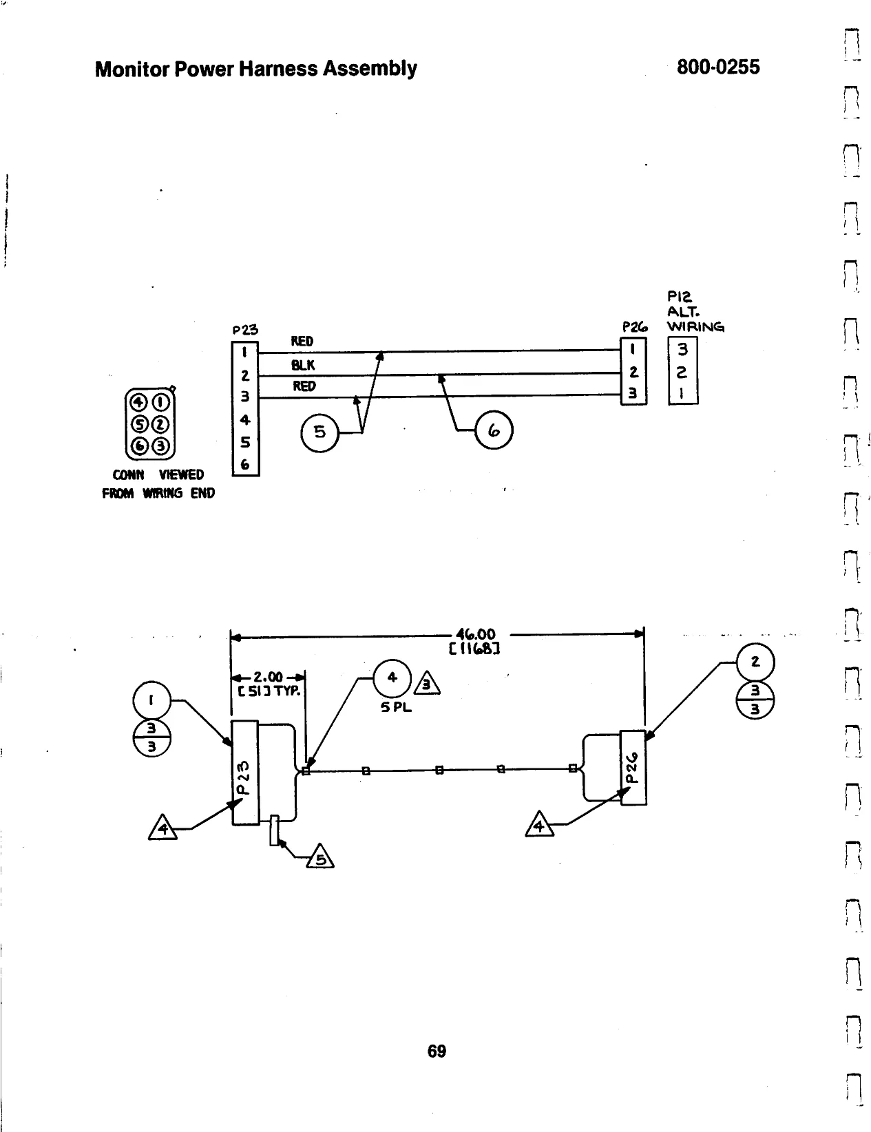
This page is a drawing, shown as the original scan.
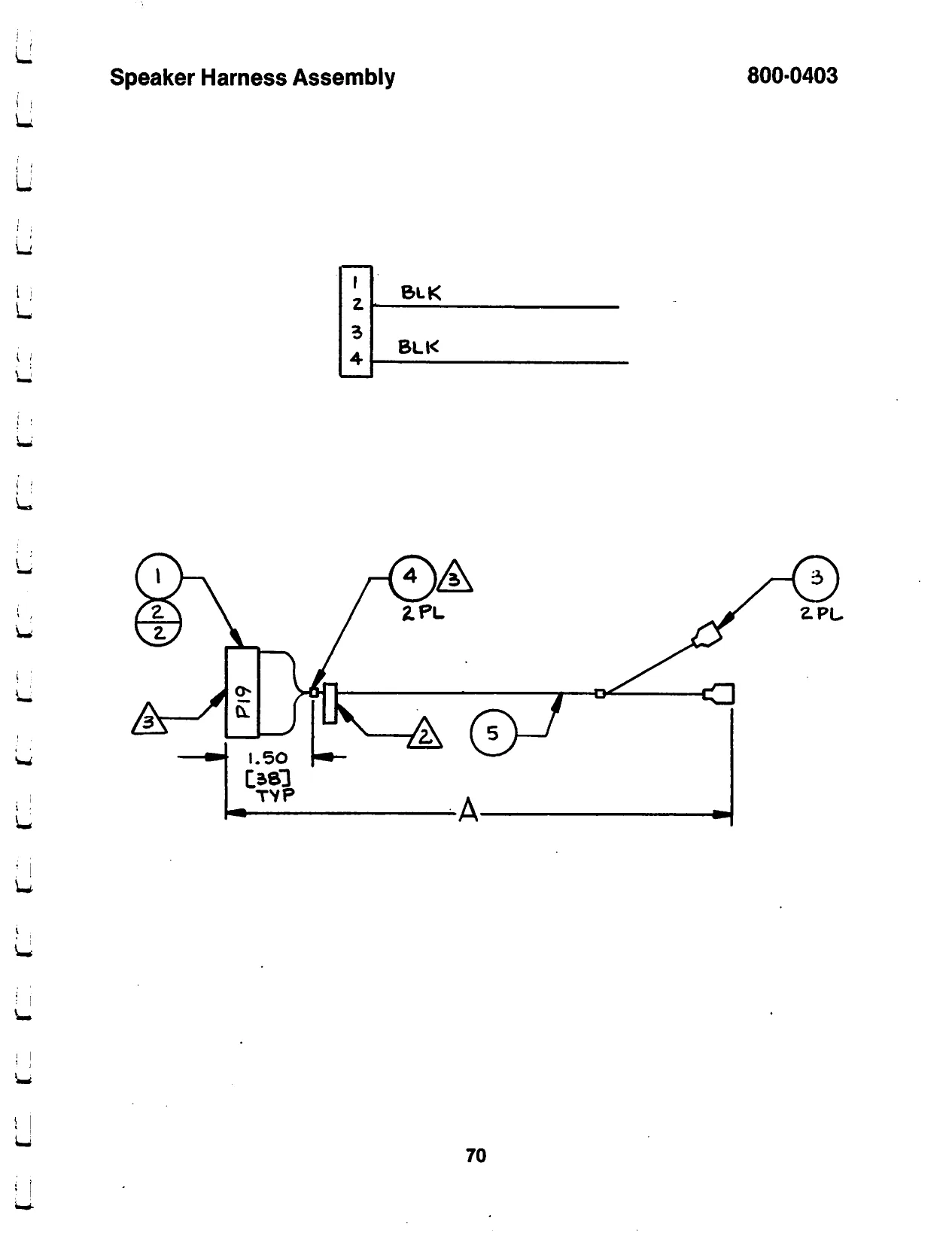
This page is a drawing, shown as the original scan.
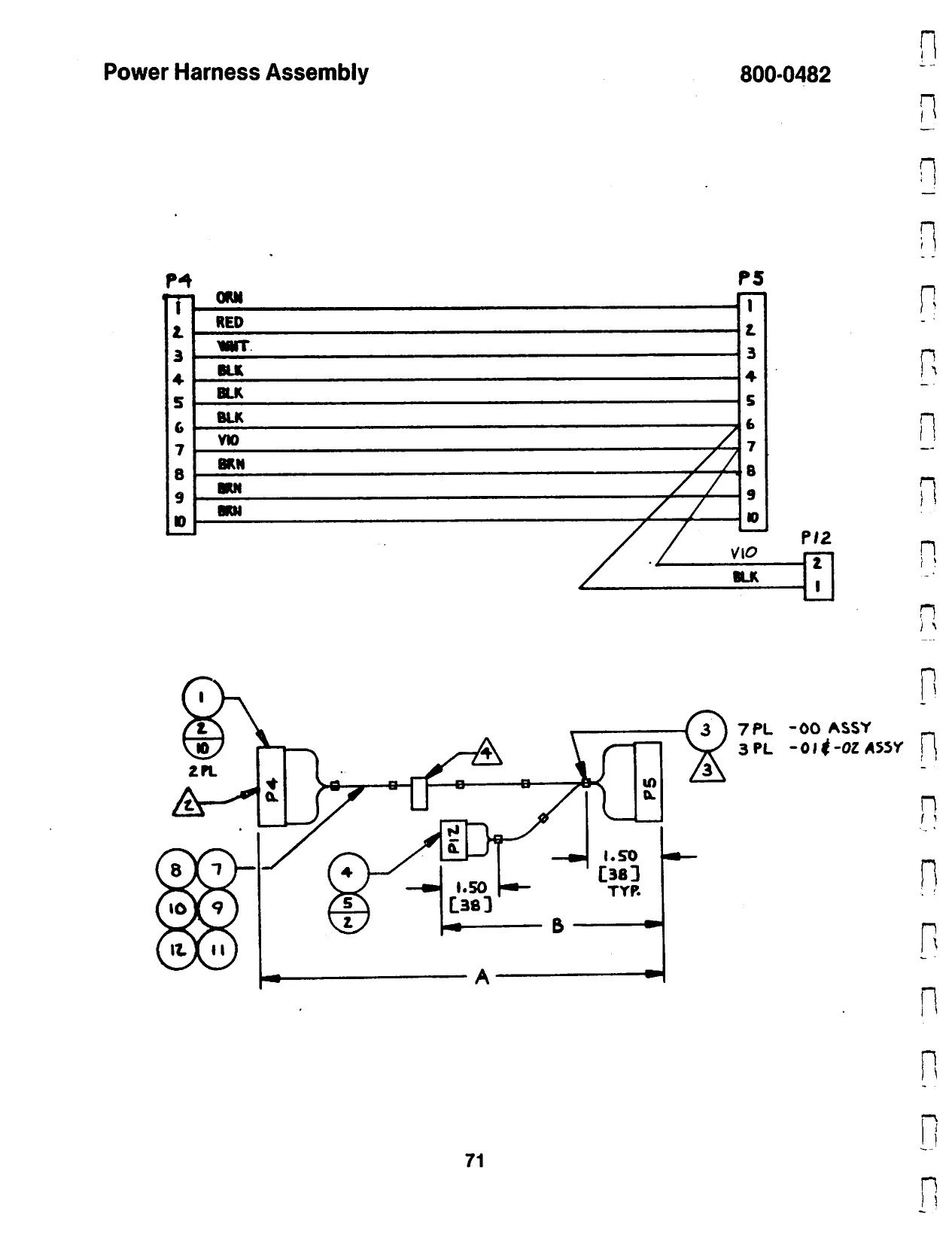
This page is a drawing, shown as the original scan.
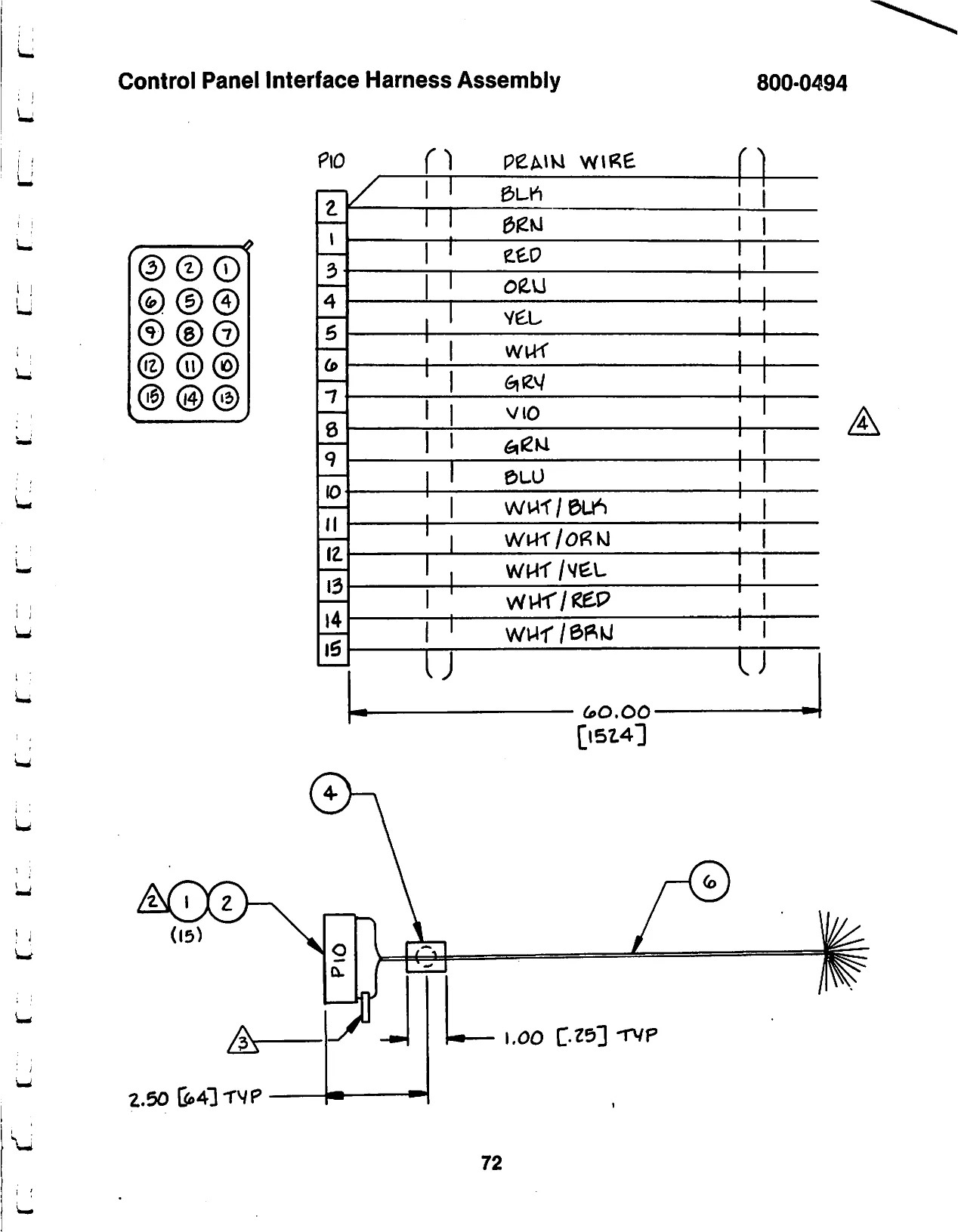
This page is a drawing, shown as the original scan.
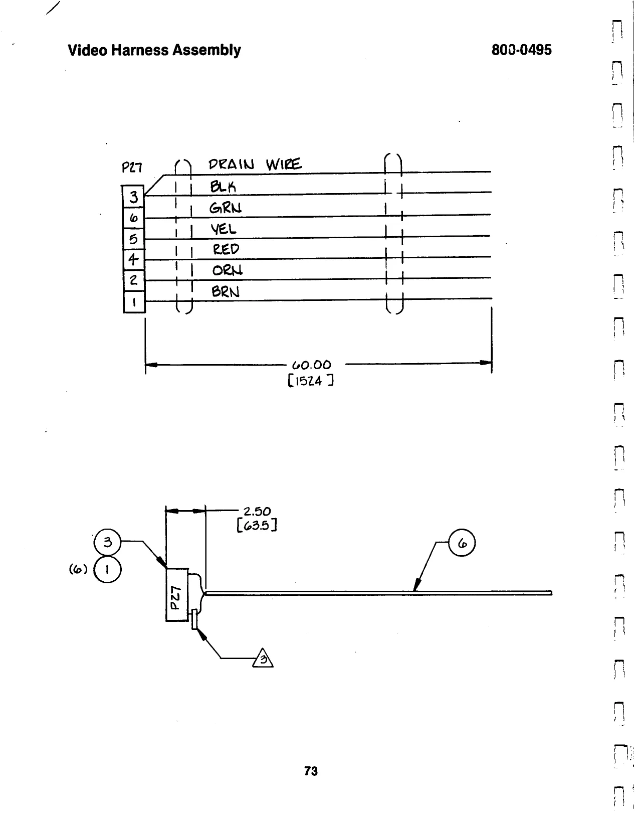
This page is a drawing, shown as the original scan.
ro rt fo TT
C
Co cl ©
i or Control Panel Harness Assembly
BLU GAY vio wut/B.v 18.00 [457.2] REO 18.00 [457.2 ] 18.00 (457.2 ] 16.00 [457.2] 18.00 [457.2] OPN 18.00 (457.2 J ye 16.00 [457.2]
BLK 16.00 [4572] 800-3423
19" X-Y COLOR MONITOR
PART NO.
EHT SUPPLY ASSEMBLY
SEMI-CONDUCTORS
315-0118
481-0211 481-0207
482-0062
482-0244
482-0030
TRANSFORMERS
560-0062
560-0073
COZLS
180-0010
CAPACITORS
150-0007
151-0053 153-0109
150-0015
151-0110
1501-0222
150-0010
156-0221 151-0113
152-0027
RESISTORS
470-0103
460-0008
470-0154
470-0123 471-0472
471-0474
460-0016 DESCRIPTION
EHT Control Circuit
Zener Diode Rectifier 1A 1400V
Transistor 3906
Transistor MPSU07
Transistor 3904
Horiz. Buffer Trans.
Horiz. Output Trans.
Horiz. Delay Choke
4.7 uf 16V
0.22 uf 50V 2000 uf 50V
22 uf 16V
0.1 uf 100V
0.022 uf 100V
106 uf 16V
High Current Cap 47 uf 160V
0.047 uf 100V
10K 1/4W 5% 47K 1/44 5% 150K 1/4H 5% 12k 1/4W 5% 4.7K 1/44 5% 470K 1/ W 5% 1.2K 1/4W 5% DRAWING NUMBER 200-0025
RES. DES.
1¢900
20903, D901
9901 Q902 Q903
T900
1901
L900
c900
C902
c903
c904
c906, c907
e911
co14, C916
c918
R900, R902
R904, R905, R907, R910
R914 901, 906
916, 934
938, 939 a
i
foe
!
lL
=)
J
t
Cn oom
on
cv:
| nn on
Cy
Co
c
Toa
cc 19" X-Y COLOR MONI TOR-Continued
PART_NO. DESCRIPTION
EHT SUPPLY ASSEMBLY CCNT'D
RESISTORS 475-0043 475-0044 470-0271
470-0471 471-0240
470-0330 470-0680 462-0001 464-0114 470-0333 470-0274 471-0475 471-0331 472-0470 470-0562 EHT SUPPLY ASSEMBLY KIT 482-0242 475-0035 EHT REGULATOR ASSEMBLY SEMI-CONDUCTORS 482-0268 482-0269 481-0204 CAPACITORS 152-0149
151-0108 472-0223 471-0683 472-0273 471-0473 200 Ohms Control
2K Control 270 Ohm 1/4W 5% 470 Ohm 1/4W 5% 24 Ohm 1/2W 5% 33 Ohm 1/4W 5% 68 Ohm 1/4W 5% 68 Ohm 1W 5% 470K Control 33K 1/4W 5% 270K 1/4W 5% 4.7M 1/2W 5% 330 Ohm 1/2W 102 47 Ohm 1W 5% 5.6K 1/4W 5%
PWR Transistor 5A 1400V Focus Control
2N 6558
TIP 47 (Motorola) IN 5263
68 pf 500V 470 pf 500V 22K IW 5% 68K 1/2W 5% 27K IW 5% 47K 1/2H 5% DRAWING NUMBER 200-0025
RES. DES.
R917
R918 R923
R924
R925 R927
R930 R932
R933 R935
R936 R937 R940
R941
R942
Q900 R922
Q320, 321, 323 Q322 70340
C330
C331 R300 R301
R302 R304
19" X-¥ COLOR MONITOR-Continued DRAWING NUMBER 200-0025
PART NO. DESCRIPTION
EXT REGULATOR ASSEMBLY CONT'D RESISTORS 470-0331 330 Ohm 1/4W 5% 471-03R3 3.3 Ohm 1/2W 5% 470-0363 36K 1/4W 5% 460-0008 47K 1/4W 5% 475-0048 10K Contro] Pot.
DEFLECTION AMP PCB ASSEMBLY
SEMI-CONDUCTORS 315-0117 Input Amplifier IC 481-0202 Rectifier 481-0020 Rectifier 1A 200V
48° -0006 Diode IN 914 481-0204 Zener Diode 1N 5263B 1/2W S6V 485-0205 Zener Diode 1N 5239B 1/2W 9.1V 483-0179 Zener Diode 9.1V 1W 5% (Motorola) 482-0248 Transistor TIB 29B 482-0244 Transistor MPSU60 (Motorola) 482-0245 Transistor 300V 1/2A
482-0243 Transistor MPSU10 (Motorola)
CAPACTORS 150-0211 100 uf 80V 150-0212 680 uf 160V 750-0213 6800 uf 80V
150-0004 10 uf 25V 151-0046 Ceramic 0.1 uf 152-0056 0.1 uf 200V 150-0220 22 uf 250V RES, DES.
R305 R306 R307 R308 R310
10600 D400-403
D404-407, 409, D408, 601-605 701-705
20400 7p401 ZD402 (1N4739) 400, 401 600, 700 601, 604, 701,
602, 603, 702,
c401 c402 C403, 404 c405 c407, 621, 721 c410
cai =
wo
‘<a
J
poet ees eee
i
an eee
co to OP
>
Co
Cl
Co © Cy
co 19" X-Y COLOR MONI TOR-Continued
PART _NO. DESCRIPTION
DEFLECTION AMP PCB ASSEMBLY CONT'D CAPACITORS 152-0145 2.2 pf 500V 152-0146 12 pf 500V 152-0147 100 pf 10% 500V 152-0023 47 pf 10% 500V 151-0107 0.068 uf 200V
152-0149 5.6 pf 10% 152-0150 560 pf 500V 20% RESISTORS 478-0006 Thermistor 120V¥ 60 Ohm 473-0330 33 Ohm 4W 10% 472-0223 22K 1M 10% 470-0222 2.2K 1/4W 5% 474-0220 220 Ohm 10¥ 471-0822 8.2 1/2W 5% 474-0680 680 Ohm 6H 470-0472 4.7K 1/4W 5% 470-0275 2.7M 1/4u 5% 470-0155 1.5M 1/40 5% 470-0621 620 Ohm 1/4W 5% 471-0911 910 Ohm 1/44 5% 470-0103 10K 1/4W 5% 470-0182 1.8K 1/4W 5% 470-0303 30K 1/4W 5% 475-0037 50K Trim Pot 470-0104 ; 100K 1/4W 5%
470-0242 2.4K 1/4W 5% 470-0102 1K 1/4W 5%
475-0038 1K Trim Pot 470-0183 18K 1/4W 5% DRAWING NUMBER 200-0025
RES. DES.
c600 603, 703 620, 720 622, 722 624, 724 c702
C725
R400 R401 R402 R403
R404 R405 R406 R410
R411 Ral2 R600 R601
R602
R603, 624, 724 R604
R605
R606
R607, 710 - R60B, 636, 637, 715, 736, 737 R611
. R620, 720
19" X-Y COLOR MONI TOR-Continued
PART_NO. DESCRIPTION
DEFLECTION AMP PCB ASSEMBLY CONT'D RESISTORS 470-0622
470-0181
470-0223
470-0101
471-0183 470-0271
471-0223 7
472-0471 479-0151 46-0056
474-0150 470-0222
475-0039 470-0153 470-0152 472-0391 4700-0475 CRT SOCKET PCB ASSEMBLY SEMI-CONDUCTORS 482-0243 LAMPS 390-0107
CAPACITORS
151-0067
151-0112 151-0050
151-0096 6.2K 1/4 5% 180 Ohm 1/4W 5%
22K 1/4W 5%
100 Ohm 1/4W 5%
18K 1/2W 10% 270 Ohm 1/4W 5% 22K 1/2W 5% 470 Ohm 2W 5% 150 Ohm 1/4W 5% 82 Ohm 1/4W 5% 1.5 Ohm 10W 2.2K 1/4W 5% 5K Trim Pot 15K 1/4W 5% 1.5K 1/4W 5% 390 Ohm 2W 5% 4.7M Trim Pot
Transistor MPS u10 (Motorola)
Lamp
100 pf 500V 0.1 uf 200V 0.01 uf 500V 10% 0.01 uf 1000V DRAWING NUMBER 200-0025
RES. DES.
R621, 721 R622, 625, 631, 722, 725, 731 R623, 704, 705,
R626, 629, 726,
R627, 727 R628, 728 R630, 730 R632 R633
R634 R635 R700, 701 R702
R703, 706 R714 R732 R930, 931
Q100-105
NE100-103
C100, 110, 130 C101 C102, 111, 131 e112, 113 ee es ee
a)
se
3°00 ea
-d 9 8
J 2
s 19" X-Y COLOR MONITOR-Continued DRAWING NUMBER 200-0025
| e | PART NO. | DESCRIPTION | RES. DES. |
il RESISTORS
| 470-0101 | 100 Ohm 1/4W 5% | R101, 112, 130 | |
| i | 470-0275 | 2.7K 1/4M 5% | R102, 113, 131 |
| a | 462-0056 | 3.3K 1W 5% | R103, 114, 132 |
| 472-0471 | 470 Ohm 1/4W 5% | R104, 115 | |
| 470-0122 | 1.2K 1/4 5% | R105, 116, 134 | |
| 475-0041 | 250 Ohm Trim Pot | R106, 117 | |
| ii | 475-0042 | 2.5K Trim Pot | R107, 118, 136 |
| 471-0222 | 22K 1/2W 5% | R108, 119, 137 | |
| L | 470-0181 | 180 Ohm 1/4W 5% | R109, 121 |
| 470-0102 | 1K 1/4M 5% | R110 |
471-0224 220K 1/2W 5% "R122
| ad | 471-0102 | 1K 1/2W 5% | R123 |
| 7 | 471-0474 | 470K 1/2W 5% | R124 |
| uw | 470-0621 | 620 Ohm 1/4W 5% | R133 |
HEAT SINK ASSEMBLY
| u | 482-0260 | 2N 6259 | Q605, 606, 705, |
| i | 260-0010 | Motor Blower Fan | M01 |
- MISCELLANEOUS
| : | 200-0040 | crt | vol |
| - | 180-0009 | Deflection Yoke | DY01 |
| 180-0017 | Degaussing Coil | L100 | |
| wu | 213-0019 | CRT PCB Socket | 3101 |
| , | 280-0208 | Yoke Wedge | X |
| u | 800-0307 | Input Limiter PCB | Xx |
| 800-0319 | Input Clamp PCB | x |
u
i 80
19” X-Y Color Monitor 200-0025
0 0° } 66 66946 5o8 E@) ‘ ‘A al ites OF
{lo Ss ui Pell o
bo, ae ou oC atl bs ip” p i “, F a i a
tp wots om $f, a wa ol = a Es a -cE- =k cc, <7 0900 = &
ae 00- vas
X-Y P.C.B. COMPONENT LAYOUT es ee eee |
727 Da 72
( €2 2 0
Cc -19” X-Y Color Monitor 200-002'5
iss. 1
cous
cole
a ass — COMPONENT ‘aot a 50-1639-02 aS "Owe 188.1 ‘a z e = lg as, = R Fae O fat 1 Oe C906 2936 One On
EHT P.C.B. COMPONENT LAYOUT
44-Pin Extension Board 176-0281
PITTI rrr)
on a a)
J
=I
J) 2
—)
J 2
tC ff.
C
- C7
C07 Cf lhe eee GAME ELECTRONICS
ITEM NO,
wont nanerwn =
- a a nun oO PART NO.
420-0560-00
420-0054-00 600-0089-00 800-0161-00 800-0163-00 800-0282-00 800-0296-00 800-0378-00 800-3307-00 800-3306-00 800-3270-00 800-0294-00 qry REQD.
ee ee ee ee ee ee ee ee ee DRAWING NUMBER 800-3305
DESCRIPTION
Decal Test Button
Decal Electronics Cable X-Y Interface Assy X-Y Timing PCB Assy X-Y Control PCB Assy Harn Video X-Y Intf Assy G-80 Gage Univ CPU Master Harn Assy Assy CPU PCB Assy 2716 Prom PCB Sound Board Assy Speech Board Assy-2732
Game Electronics Assem
c-
en
- Co G-80 CAGE UNIVERSAL ASSEMBLY
ITEM NO.
AnaPrwn PART NO.
250-0456 250-0499 280-0343 420-0560 800-0105 281-0045-06
281-0001-12
281-0001-06
284-0001-00 Qry REQD.
o-2748n = DRAWING NUMBER 800-C296
DESCRIPTION
G-80 Cage Assembly G-80 Cage Bracket Split Grommet Test Button Decal 6-Slot Master Board Assembly Pan Head Phillips Screw, Type AB, 10-12 x .375 Lg Pan Head Phillips Machine Screw, #4-40 x 3/4 Pan Head Phillips Machine Screw, #4-40 x 3/8 Flat Washer, #4
Cc
cc
i
u 800-0296
G-80 Cage Universal #2 Assembly
CZ Cl CY Ce
Cee eer
Cc
c=
a Os One Cane Gu CPU BOARD ASSEMBLY ~
ITEM NO. PART. NO.
800-0107-02 316-1873-00 315-0064-00 Qry REQD. DRAWING NUMBER 800-2307
DESCRIPTION - REF DES.
CPU Board Assy IC EPROM 2716 -U25 Chip 315-0064
CPU BOARD ASSEMBLY
ITEM NO. PART NO.
150-0088 151-0005 151-0012 151-0020
151-0060 aOpwn
151-0061 170-0194 211-0008 212-0098 10 230-0013 11 314-0001 12 314-0015 13 314-0018 14 314-0019 15 314-0055 16 314-0058 7 314-0062 oon on
18 314-0066 19 314-0067 20 314-0068 21 314-0078 22 314-0083 23 314-0085 24 314-0087 25 314-0093
26 314-0099 27 314-0105 28 315-0041 29 315-0046 Qry REQD.
nN =s3o- sw
wo a o-ow we Paso ao BP po
Po Pe BP ew Hew HO DESCRIPTION
Cap E 10 uf 25V Cap CER 680 pf 50V Cap CER .1 uf 50V Cap CER 33 pf 50V Cap CER .1 uf 16V AX
Cap CER 220 pf 16V AX PC Board Conn Pin Test PT Conn 4 10 Pin RTA XTAL 8,000 MHZ IC NE555
Ic 7404 IC 74Ls00 1G 74LS04 Ic 748244 1c 74LS08 IC 74L874
IC 74L827 IC 74LS30
IC 74L932 Ic 74Ls 2 1c 74.8240 IC 74814 IC 74L$139 IC 74L$374
TC 74.8245 TC 74LS253 IC Z80A Tc 2114 DRAWING NUMBER 800-0107
REF DES.
C43, C46, C62 c50 C47
cag (37-042, C44, C48, C51-C61, C63, C64 C1-C36
TP1-TP4
YI ui2 U30 U6, U8, U14, U9 us U34, U36, U38 U3 U10, U11, U17, U20, U39 U16 U37 U32, U33 U23 U4
U7, U3) v24 U3
U35 Ul, U2, U5, U9 U22
U26-U29 “1 24 2) I
=
+
a3 2
CPU BOARD ASSEMBLY-Continued
ITEM NO. PART NO.
315-0050 316-0764
390-0003
471-0101
471-0102
471-0103
471-0104
471-0122
471-0220
471-0221
471-0331
477-0002
481-0001
481-0006
482-0006 482-0010
482-0014
510-0052 510-0053
213-0001
213-0002
213-0004
213-0005
510-0049
471-0472
280-0420
471-0473
151-0031 QTY REQD.
—--]|-n | Sse nee kh SBP eo ae aANnNABtA nN WOoOWwAtaBtweno ew DESCRIPTION
IC 2516 (2716) IC Prom 32x8
Led Red Res 100 Ohm 1/2W 5% Res 1K Ohm 1/2W 5% Res 10K Ohm 1/2W 5% Res 100K Ohm 1/2W 5% Res 1.2K Ohm 1/2W 5% Res 22 Ohm 1/2W 5% Res 220 Ohm 1/2W 5% Res 330 Ohm 1/2W 5% Res Pack 15x2.2K
Diode 1N4002
Diode 1N914/1N4148 XSTR N4403
XSTR PE8050
XSTR N4401
SWITCH PIANO DIP SW Pushbutton Side PCM SKT 24 Pin Dual INLN
SKT 18 Pin Dual INLN
SKT 16 Pin Dual INLN
SKT 40 Pin Dual INLN Switch 8 Pos Dip Res 4.7K Ohm 1/2W 5% Card Ejector, Snap On Res 47K Ohm 1/2W 5% Cap CER .22 uf 16V DRAWING NUMBER 800-C107
REF DES.
U25
UIs
D3
R5 RI, R3 R6
R7, R8, R22 R12
R14
R2, R4, R13 R10, R11, RI5-R20 RP1-RP3
DI, D2 D4
Q7 Qi, Q2 Q3-06, 08 SWI SW3 xU25
XU26-XU29
XUIS
XU2T, XU22 Sw2 R21
RO c45
C~ f= CZ CH 800-0107
CPU Board Assembly
(0 0N9e | JOU 0° Yoooo JOU 4 U0 if ial 00g. 3 "0000 mnie ae a a ES \ GOR ROUIOOG HeNsONO NG it veh HH YS
Cc
CT
Cc ( fe fe a 2716 PROM BOARD ASSEMBLY
ITEM NO.
wnt nner wn a
NNYA NHN HS Be ewe owe won PWN OCH ANA NP WH =| OC PART NO.
800-0151-00
316-1848-00
316-1849-00
316-1850-00
316-1851-00
316-1852-00
316-1853-00
316-1854-00
316-1855-00 316-1856-00 316-1857-00
316-1858-00
316-1859-00
316-1860-00
316-1861 -00 316-1862-00
316-1863-00 316-1864-00
316-1865-00
316-1866-00
316-1867-00
316-1868-00
316-1869-00 316-1870-00 Qry REQD.
ee ee ee ee ee a ee ee ee ee ee oe DRAWING NUMBER 800-3306
DESCRIPTION
Assy G-80 2716 PROM Board IC EPROM 2716
IC EPROM 2716
IC EPROM 2716
IC EPROM 2716
IC EPROM 2716
IC EPROM 2716
IC EPROM 2716
IC EPROM 2716
IC FPROM 2716
IC EPROM 2716
IC EPROM 2716
IC EPROM 2716
IC EPROM 2716
IC EPROM 2716
IC EPROM 2716
IC EPROM 2716
IC EPROM 2716
IC EPROM 2716
IC EPROM 2716 IC EPROM 2716
IC EPROM 2716
IC EPROM 2716
TC EPROM 2716 REF DES.
LU}
u2
U3
U4
Us
U6
U7
us
ug
ul0
ui
ul2
U13
u14
ums
U16
ul7
u18
hE)
U20
v21
U22
U23
G-80 2716 EPROM BOARD ASSEMBLY
ITEM NO. PART NO.
1 151-0058
2 ‘151-0060
170-0211
213-0001 314-0055 314-0058 314-0059 314-0104
314-0120
10 211-0008 W 150-0088 wow nrtan & w
12 280-0420 QTY REQD.
=—weran stow DESCRIPTION
Ceramic Capacitor, .01 uf, 16V AX
Ceramic Capacitor, .1 uf, 16V AX
PC Board 24-Pin Dual Inline Socket
IC 74LS244 IC 74LS08 IC 74LS10 IC 74.8138 IC 74LS154 Test Point Connector Pin
Electrolytic Capacitor, 10 uf, 25V Card Ejector, Snap On DRAWING NUMBER 800-0151
REF DES.
C2, C4, C6, C8, C9, C11, C14, C16, C18, C21, C23, C25, C27 C1, C3, C5, C7, C10, €12, C13, C15, C17, C19, C20, C22, C24, C26, C28
XUT-XU23
U25
U26-U28 u29 U30 U24
TP1-1P3
cao
Varad oo Ue NOOO GUO 000 OO00 O00 OO00 2S) 272 29 2 dd dd ed ed
X-Y TIMING ASSEMBLY
ITEM NO. PART NO.
1 151-0005 2 151-0058 3 170-0218 4° 211-0008
5 212-0101 6 213-0001
7 213-0004 8 213-0010
9 230-0009 10 280-0420 u 313-0037 12 313-0044 13 314-0018 4 314-0019
15 314-0040 16 314-0046 Ww 314-0055
18 314-0058 19 314-0062
20 314-0070 21 314-0073 22 314-0074 23 314-0076
24 314-0078 25 314-0093 26 314-0097
27 314-0101 28 314-0108 29 314-0120 30 314-0135 qry REQD.
nD a aOnwtae MBA nnNNM AND WH eo
“Sse ear et ane = DESCRIPTION
Cap CER 680 pf 50V Cap .01 uf 16V AX PC Board
Conn Pin Test PT Conn 4 Pin M RTA
SKT 24 Pin Dual INLN
SKT 16 Pin Qual INLN
SKT 8 Pin Dual INLN Xtal 15.46848 Card Ejector IC TLO81 CP IC AD561 IC 74LS00 IC 74.804
IC 74.8125 IC 74LS04 IC 7418244
IC 74LS08
IC 74L874
IC 74.886 IC 74LS175 IC 74.8191
IC 74LS157
IC 74LS02
IC 74LS374
IC 74LS161
IC 74L$283 IC 74.8107 IC 748154 1c 74811 DRAWING NUMBER 800-0161
REF DES.
c7
C1-C3, C6, C8-C28
TP
XP1, XU39, XUSO XUT, XU4 XU2, XU3 Yi
U2, U3 ul, U4 v28
u30, u40 u27 u14 U54, U57, U58 U13, v21 u25, U26, U42, U43, us2 u29 U35-U38 U15-U20 U5-U10
U53
U48, U49, U55, US6 U31-U34, 41, USI U44-u47 UIT, U22-U24 u50 ui2
| no
C X-Y TIMING ASSEMBLY-Continued
ITEM NO. PART NO.
315-0019 471-0202 471-0331 471-0392 475-0024 151-0008
150-0088 151-0042 481-0006 151-0002
314-0068 Qry REQD.
- YUNA DA NNNDND = DESCRIPTION
IC 2708
Res 2K Ohm 1/2W 5% Res 330 Ohm 1/2W 5% Res 3.9K Ohm 1/2 5% Pot 1K 10 Turn Cap CER .001 uf 50V Cap E 10 uf 25V RDL Cap, Cer 470 pf 50V 1N914 Diode Cap CER 100 pf 50V IC 74L$32 DRAWING NUMBER 800-0161
REF DES.
U39
R2, R4 R7, RB R1, RS R3, R6 C29, C30 ca, C5 C31 DI, D2 C32, C33 U59
i ae ee el jontl] Ooong oo (oon no0 ood fooo ooood Mono. ‘ooghns Cn Eo 800-0161
X-Y Timing Board Assembly
C2
Cy
| rn
CT
- on
| om
ee Green Gane Ge
Cc
t= X-¥ CONTROL ASSEMBLY
ITEN NO. PART NO.
150-0088 151-0002 151-0058 170-0219 212-0101 213-0001 280-0330 314-0018 314-0019
314-0040 314-0055
- a =-OFCv On an ePwn —
12 314-0058 13 314-0059 14 314-0060 15 314-0062 16 314-0067 7 314-0068
18 314-0074 19 314-0075 20 314-0078 2 314-0087 22 314-0093
23 314-0097 24 314-0099 25 314-0101 26 314-0108 27 314-0127 28 314-0128 29 314-0137
- 315-0046 Qry REQD.
nN su =
sworn eto
onereonesosane towne nano DESCRIPTION
Cap E 10 uf 25V Cap CER 100 pf 50V Cap CER .01 uf 16Y AX PC Board Conn 4 Pin M RTA
SKT 24 Pin Dual INLN
Card Ejector IC 74LS00 IC 74LS04
IC 74L8125 Ic 74LS244
IC 74LS08 IC 74LS10 IC 74L$20 TC 74LS74
IC 74L$30 IC 74LS32
IC 7418191 IC 74LS393 IC 74LS02 IC 74L$139 IC 74LS374 IC 74LS161 IC 74.8245 IC 74LS283 IC 74LS107
IC 74.8164 IC 74.895 IC 74LS09 IC 2114 DRAWING NUMBER 800-0:63
REF DES.
C23
c14 C1-C13, €15-C22
xP1
u40 U9, U32, U42 U39 U20, U21, U35, U36, U48, U49, U54 U37 U18, U4) U50 u19, U5] U47
U4, U38 U15-U17 u22
U46 U2, U13 U10-U12, U34,, U52 u14
U33
U5S3
U3 U6, U7, U44, U45 Ul, US U24-U31
X-Y CONTROL ASSEMBLY- Continued
ITEM NO. PART NO.
315-0072 471-0123
471-0472 471-0622 481-0006 212-0002 4n-0471 471-0103
471-0332 471-0512
482-0006 482-0014 Qry REQD.
—- wee nn gaaw-wsn DESCRIPTION
IC AM25LS14
Res 12K Ohm 1/2W 5% Res 4.7K Ohm 1/2W 5% Res 6.2K Ohm 1/2H 5% Diode 1N914/1N4148 Socket 18 Pin Res 470 Ohm 1/2W 5% Res 10K Ohm 1/2W 5% Res 3.3K Ohm 1/2W 5% Res 5.1K Ohm 1/2W 5% XSTR 2N4403 XSTR 2N4401 DRAWING NUMBER 800-0163
REF DES.
U8, U43 RI, R3, RS R7
R2, R4, RG D1-D6
XU24-XU31 R8 RO R11
R10 qi Q2 a
=I
800-0163
X-Y Control Board Assembly
| Bento 7 OU ol “O01 nh ‘ooll fooag Whdoogioc
UNIVERSAL SOUND BOARD ASSEMBLY
ITEM NO. PART NO.
150-0087 150-0090 150-0135
151-0002 181-0021
151-0060
151-0011 152-0085
152-0144 170-0259 212-0081 213-0001
213-0022
213-0005 230-0037 280-0420 313-0037 313-0038
314-0018
314-0055
314-0060
314-0062 314-0067 QTY REQD.
nner
eno
ee DESCRIPTION
Cap-E 4.7 f 25V ROL Cap-E 33 f 25V RDL Cap-E 1 f 25¥ RDL
Cap-CER 100 pf 50V Cap-CER 20 pf 50V Cap .1 f 16V AX
Cap-F .15 f 50V Cap-F .01 f 50V
Cap-F .082 f 50V PC Board Conn 4 Pin M RTG PLZD Skt 24 Pin Dual INLN Skt 18 Pin Dual INLN
Skt 40 Pin Dual INLN
XTAL 6.0 MHz Card Ejector Snap On IC TLO81 IC TLO82
TC 74LS00 IC 74.8244
IC 74LS20 Ic 74LS74 IC 74LS30 DRAWING NUMBER 800-0377
REF DES.
cl, c4 c60 C14, C15, C33-C36, c54 C6-C8, C19-C24 cal, c42 €3, C5, C10-C12, C18, C26-C31, 37-C40, C43-C50, (57-C59, C61, C62 C51, C55, C56 c9, C13, C16, CI7, C25, C32 (53
PI XU50, XU5I XU44, XU45
XU46 Yi
u4ag U1, U3-U6, U9, U17-U23 U36
U55
u40 U2, U38 U5S9 i J a 4
i
co
J
mo
ees
om
Co
C7. ©. fo fo TT UNIVERSAL SOUND BOARD ASSEMBLY-Continued
ITEM NO. PART NO.
314-0068 314-0075 314-0076
314-0085 314-0087 314-0099 314-0100 314-0104 314-0131 315-0035
315-0046 315-0059 315-0077
315-0079
315-0132 315-0133 470-0102
470-0103
470-0104
470-0105 470-0124 qry REQD.
Ar- wnt tee Nn wn w
no
B DESCRIPTION
IC 74LS32 IC 74L$393
IC 74LS157
Ic 74.814 IC 74LS139 IC 74LS245 IC 7418273 IC 748138 IC 74LS373 IC MM5837
IC 2114 IC 8253 IC 8035
IC CD4053
IC AD7524
IC 2k x 8 Static RAM Res 1K Ohm 1/4W 5%
Res 10K Ohm 1/4W 5%
Res 100K Ohm 1/4W 5%
Res 1M Ohm 1/4W 5% Res 120K Ohm 1/4W 5% DRAWING NUMBER 800-(:377
REF DES.
U35, U37, U39 U32, U33 U56-U58
ulo, WI U52, U53 u54
u34 v47
u60 u44, u45 u41-u43 u46
U7, U8, U15, U16, U30, U31 U12-U14, U24-u29 U50, USI R23, R24, R30, R33, R53, R56, R59, R6S R20-R22, R27, R40, R41, R50-R52, R57, R58
RI, R7-R10, R12, R13, R15, RIG, R18, R19, R25, R28, R29, R31, R32, R34-R36, R38, R39, R42, R43, R45, R46, ROS, R49, R54, R55 R2, RV R6
UNIVERSAL SOUND BOARD ASSEMBLY-Continued
ITEM NO.
49° PART NO.
470-0222
470-0271 470-0272 470-0333 470-0334
470-0562
470-0332
482-0023 182-0054
152-0076
212-0158
212-0159 QTY REQD.
eee se sae wer erm Dn DESCRIPTION
Res 2.2K Ohm 1/4W 5% Res 270K Ohm 1/4W 5% Res 2.7K Ohm 1/4W 5% Res 33K Ohm 1/4W 5% Res 330K Ohm 1/4W 5% Res 5.6K Ohm 1/4W 5% Res 3.3K Ohm 1/4W 5% XSTR 2N4093 Cap-F .001 f 50V Cap-F .1 f 50¥ Conn Header 8 Pos
Conn Jumper DRAWING NUMBER 800-0377
REF DES.
RS, R60 R62 R64, R65 R14, R37, R44, RET R3
RI7, R26, R47 R4 qi c2
P2
os eee |
a
on |
= me all Cop wWolgto fot i
vin = U0 l-0o000
Ele = ® CO () 00 aan TU 00 t__) I
Universal Sound Board Asseinbly
800-0377
SPEECH BOARD ASSEMBLY
ITEM NO.
Pwn PART NO.
800-0294-00 316-1607-00 316-1871 -00 316-1872-00 QTY REQD.
- oe oo DESCRIPTION
Assy 2732 Speech PCB IC EPROM 2716 IC 2732
Ic 2732 DRAWING NUMBER 800-3308
REF DES.
U7
U6
us (J (23 a
a
(Za
i
fa co eo
t (2 mo
(=
C-
om
Cc
Co
on
| oa
r
i
CZ SPEECH BOARD ASSEMBLY
ITEM NO.
aOrwn
wo naan PART NO.
150-0087 150-0088
151-0021 151-0056
151-0058
151-0060 170-0223
212-0012
230-0033 280-0420 313-0037
313-0038
314-0058
314-0062 314-0067 314-0072 314-0085 314-0087 314-0100 314-0042 314-0131
315-0061 315-0077 315-0079 316-0788 471-0103
471-0106 471-0222 471-0223 471-0274 Qry REQD.
-na-
= o
ee © a Se a Ce DRAWING NUMBER 800-0294
DESCRIPTION
Cap E 4.7 uf 25V Cap E 10 uf 25V Cap Cer 20 pf 50V Cap Cer .047 uf 50V Cap Cer .01 uf 16V AX
Cap Cer .1 uf 16V AX PC Board
Conn 6 Pin M
Crytral 3.12 MHZ Card Ejector IC TLO8] CP
IC TLO82 CP
IC 74LS08
IC 74L874 IC 74.830 IC 7418174
IC 74L$14 IC 74LS139 IC 74.8273 IC 7406
IC 74.8373
IC ST-32034 IC 8035
IC CD4053 IC Prom Speech Bd Decoder Res 10K Ohm 1/2W 5% Res 10 Meg Ohm 1/2W 5% Res 2.2K Ohm 1/2W 5% Res 22K Ohm 1/2W 5% Res 270K Ohm 1/2W 5% REF DES.
c2
C13, C46-C49 c6, C7 C10
C5, Cli, C12, C14- 17, C19, C20, C44 C9, C37, C38
YI
Snap On us
ull
U35
u1s
U37
U38 u10 v2 u13
ug
v2
u14
ul2
U30 R17, R21, R27-R29 R3 . R24 R13, R14, R18, R22 R19
SPEECH BOARD ASSEMBLY-Continued
ITEM NO.
34° PART NO.
47-0471 477-0002 471-0683 475-0022 151-0009
471-0472
21 -0001
213-0004
213-0005 213-0008
213-0010 213-0012 471-0102 Qqry REQD.
Pn Ce Ce ee ee ee ee DESCRIPTION
Res 470 Ohm 1/2W 5% Res Pack 15x2.2K Res 68K Ohm 1/2W 5% Pot 100K 10T PC MNT Cap Cer .003 uf 100V Res 4.7K Ohm 1/2W 5% SKT 24 Pin Dual INLN SKT 16 Pin Dual INLN
SKT 40 Pin Dual SKT 20 Pin Dual INLN
SKT 8 Pin Dual INLN SKT 28 Pin Dual INLN Res 1K Ohm 1/2W 5% DRAWING NUMBER 800-0294
REF DES.
R25, R26 RP2 R30
R74 cs0
R20
XU3-XU7
XU30 xU14
xU9, XU21 xU8, XU11 xu2 R75 =I
I~
a]
eee Ree
3 ico
ca
=)
(— fl fh ce ee oe ee
Co Ch co
Cc ce
Cc
Cc cS co
ct Speech Board Assembly _ 800-0294
G-80 POWER SUPPLY CHASSIS ASSEMBLY
ITEM NO.
Aan Pwn —
ow
am PART NO.
530-0016 250-0460 250-0461 800-0170 253-0206
281 -0032-06
482-0104
313-0023 313-0014 313-0015
482-0100
482-0019
420-0557
280-0117
420-0575 281-0001 -08
280-0341 -00 310-0006-01
284-0001-00 284-0031-00
283-0021-00
800-0243 qy REQD.
a onnawa
ao-- = DRAWING NUMBER 800-0191
DESCRIPTION ” REF DES.
Heat Sink, G-80 Pwr Sup. Chassis Support Cover
PCB Assembly PCB Support, Threaded Thread Forming Screw, #6 Type B, 3/8 long
Power Transistor TIP 141 Negative 5 Volt Regulator 320T5 Positive 12 Volt Regulator 340T12 Negative 12 Volt Regulator 320T12 Power Transistor (Audio Amp) TIP 125 Power Transistor (Audio Amp) TIP 120
Fuse Decal Tab Rivet Male 1/4" Power Supply B Decal Pan Head Phillips Screws, 4-40x1/2" Lg Shoulder Washer, #4 Transistor Insulator, 10-220 Flat Washer #4 Split Lock Washer #4 Machine Hex Nut, 4-40 G-80 Transistor Harness
Assembly P1 es |
=
poe
a
I
=
Ta 24
noon
eae)
d
poe
i
to
t
C
CO CS eT
C2: G-80 POWER SUPPLY CHASSIS ASSEMBLY-Continued
ITEM NO. PART NO.
800-0244
800-0245
800-0246
800-0247
800-0248
310-0007-01
600-0092-42 600-0092-45
600-0092-49 310-0041-02 280-0407 Qry REQD.
5" 5" 5¢ 3" DRAWING NUMBER 800-0: 91
DESCRIPTION REF DES.
G-80 Transistor Harness Assembly, P2 G-80 Transistor Harness Assembly, P3 G-80 Transistor Harness Assembly, P4 G-80 Transistor Harness Assembly, P5 G-80 Transistor Harness
Assembly, P6 Transistor Insulator "H", TO0-218 Wire, 22 Awg Red Wire, 22 Awg Green Wire, 22 Awg White Tubing, Shrink, .125 ID Clear Cable Tie
G-80 Power Supply Chassis Assembly
-2o use (3) “02 asey
ACK SIDE OF MEAT SINK item D
cucuir sick ono Vem # 800-0191
VIEW ‘A“ TYP. ata (ace) I
=
Ce
C
Go ro fcc
Cy Gt
on rn On a G-80 POWER SUPPLY PC ASSEMBLY
ITEM NO.
iW PART NO.
150-0088
150-0092
150-0095
150-0096
150-0097
151-0002
151-0007
151-0011
151-0012
151-0021
170-0222 212-0020 212-0081 313-0001 471-0011 471-0101
471-0102 471-0103 471-0104 471-0222 Qry REQD.
w
NR] NM WoO] Bow Dw | DRAWING NUMBER 800-0170
DESCRIPTION
Electrolytic Capacitor, 10 uf, 25V
Electrolytic Capacitor, 100 uf, 25V Electrolytic Capacitor, 3300 uf, 25V Electrolytic Capacitor, 6800 uf, 16V Electrolytic Capacitor, 4700 uf, 25V Ceramic Capacitor, 100 pf, 50V Ceramic Capacitor,
- 005 uf, 100V Ceramic Capacitor, -O1 uf, 50V Ceramic Capacitor, -1 uf, 50V Ceramic Capacitor, 20 pf, 50V PC Board 10-Pin Male Connector RTA 4-Pin Male Connector RTA IC LM723 Dip Resistor, 10 Ohm, 1/2W 5% Resistor, 100 Ohm, 1/2W 5% Resistor, 1K Ohm, 1/2W 5% Resistor, 10K Ohm, 1/2W 5% Resistor, 100K Ohm, 1/2W 5% Resistor, 2.2K Ohm, 1/2W 5% REF DES.
c5, C8, C10, C18, C19, C23, C24, C26, C31 C17
C30
C32-C34
C15, C16, C27, C28 co
C20
C21, C22, C25, c29
C2, C13, C14
c7
Mm R2
R320 RIO, R27, R29 RG, R30 R23 R21, R22
G-80 POWER SUPPLY PC ASSEMBLY-Continued
ITEM NO.
23,
_ 36 PART NO.
- -0223
471-0332
471-0182
471-0681
473-05R0 473-00R2
475-0004 481-0002 481-0004
481-0006
482-0006
482-0014
514-0002 514-0003 514-0001
514-0073 800-0191 471-0220 47-0221 Qry REQD.
nen eee on
o
—-=s=s42/2 =] Q0N NPL W DESCRIPTION
Resistor, 22K Ohm, 1/2W 5% Resistor, 3.3K Ohm, 1/2W 5% Resistor, 1.8K Ohm, 1/2W 5% Resistor, 680 Ohm, 1/2W 5% Resistor, .05 Ohm, 5W 32 Resistor, .2 Ohm, 3W 5% Pot 1K Car PCMTV Diode MR751 Diode MR501
Diode 1N914/1N4148 Transistor 2N4403 Transistor 2N4401
Fuse 3A Norm Clip Fuse Mounting Fuse 2.0 S.B°
Fuse 15A Slow Blow Schematic Reference Resistor, 22 Ohm, 1/2W 5% Resistor, 220 Ohm, 1/2W 5% DRAWING NUMBER 800-0170
"REF DES.
R5, R9 R28
R26
R7 R25
R14, R15 R31
DIO, DI2 D6-D9, DII, D13-D17
DI, D4, DS Ql, Q7 Q2, 93 FI, F2
Fa F3
R8 R33 =
ad
on
=
“zd
=
7a
q a
| oon wane
CT
C2
Co
Cz
G-80 Power Supply PC Assembly
800-0170
=02 AND = 03 ASSY = eee
cme ere ee ee ere ee ee ee
Schematics
C
Co
Cc
Co
| an
Cl
C2
Cc
a 44-Pin Extension Board Signal “Pin-outs” 44-Pin Extension Board
Control Panel (P10-5) Control Panel (P10-3) Control Panel (P10-12) Control Panel (P10-15) Control Panel (P10-6) Control Panel (P10-9) Control Panel (P10-11) Control Panel (P10-10) Control Panel (P10-7) Control Panel (P10-4) Control Panel (P10-8) Control Panel (P10-13) Control Panel (P10-14) GND (P10-2) GND [|
GND Control Panel (P10-1) |_| . GND [| Reset — (N.O.) Counter A Counter A — (+5V) Counter B Counter B — (+5V) Coin B — (N.0O.) Coin B — (N.C.) Coin A — (N.O.) Coin A — (N.C.) Service — (N.O.) Service — (N.C.)
Audio Volume GND R G B . , GND
“eyes
wy GND otro rInnmomaosow Dn Pb
za YEL RED WHT/ORN WHT/BRN WHT GRN WHT/BLK BLU GRY ORN Vio WHT/YEL
WHT/RED BLK
| > Extra GND Sources
Not Internally Connected BLK WHTIYEL WHT/IORN WHT/BRN ORN BRN YEL BLU RED WHT
vio GRY GRN BLK RED GRN BLU BLK WHT
GRY BLK 170-0281
This page reads as a drawing: its text was drawn rather than typeset, and comes out in fragments. See the original scan.
EMI Transformer Assembly
ITEMS 2PL P25 (gee 800-0190
t BLK 3.00 76 [-nwas ows]
Pi AC Junction Box Assembly 800-0145
TO TRANSFORMER
suo, | atk.
GND STUD -—_____ | BR INTERLOCK | \ orn 3
SWITCH 5
ow ~T | = | 2 = | og \ Ey z /
| | | x | zx! |
al 6/3! i
| Il | _ | BLK | | |
' —]
| Lo ' =
| l | a | }—_--— |
FUSE HOLDER i |
Ac PLUS
Game Electronics Assembly
ITEM rem 800-3305
#10 ITEM iTEM #9 a4 J
ITEM #3 PART OF ITEM #6
r/o Jar" #6
FIRE
THRUET
THRUET
FIRE
Z PLAYER
) PLAYER
74L5 393
N\ U4 7ELSIFA
THL O74 REVISIONS DESCRIPTION ‘APPROVED SHT 1 t DATE,
‘CODE IDENT NOMENCLATURE PART OR IDENTIFYING NO. OR DESCRIPTION
FRACTIONS DECIMALS = XX = XXX = PARTS LIST
ANGLES ‘San Dago. Celorna 92129 = a Single Player Control Panel Interface frente of Gece [F-62 | a
NEXT ASSY USED ON SIZE ] CODE IDENT NO. [DRAWING NO. 800-0374
APPLICATION
This page reads as a drawing: its text was drawn rather than typeset, and comes out in fragments. See the original scan.
This page reads as a drawing: its text was drawn rather than typeset, and comes out in fragments. See the original scan.
This page reads as a drawing: its text was drawn rather than typeset, and comes out in fragments. See the original scan.
This page reads as a drawing: its text was drawn rather than typeset, and comes out in fragments. See the original scan.
2 | 30 3 REVISIONS
| mann” | “ve | ie | BESCRIPTON | are | APpnoveo |
| &)<8) | +5 | [ [sae sat. | XD | |
| BO | 4 | : | _ |
alse g
| - | im | + |
| oan | AZ Hof, ——__ | _ a |
| 71 | S laa cot | a |
| | | 4 | 3 |
+ Jaq U3d 2 -
| \ | 3 Jas 2708 | tt | ms | |
| 1 | 2S st | — | ||
| | | a7 we} | t + | ||
| Li] | i FEW | 7 tT | __ | | |
| fa, jeviee 7s | | eat | 1 | 1 lerhaale, 7/6 | |
| 4 | ee | 8 | ||
| uss | in | rf | I | 48 |
| SYM | | | a | aLs374 | |
| 9 [Te ayalsyepa | e | eoocnon |
y
| 1 | 1 | th | |||
| . | rr | i | + | | | onaw |
| +7
| a | 1 | ‘71500 | ||
| + | i | se | — | |
| f | - | “gfe, —__(@) at | ||
| | | 4 | | | Biya) | |
| : | oe | 1 | ||
| in | 1 | | | ||
| im | i|l | ty | yas a | va |
| ia | = | 4 | ||
| Lo | 4 | + |
= tT
| = | TT | t |
{ |
| I | 1 | | | |
| 4 | tf | 4 | | |
] |
| | | slo ale balsa | sl salts | |
| | | uaa | a] vas | 2 7a1S00 |
| 7aLS263 | 7415283 | a |
Sit
| 4 is | Ie yt da | 30 | 13 744800 7 |
| 7 | | | 74Ls04 12 U28 | YCL, |
| - | = | w | |
| { | i | 45 |
| 8
| ls | teat, , | [a | ||||
| 4 | 7 | 4 7| U3S | { | | | 741574 | |
| 5 | 5 | 10) 7415175 | a7 | |||
| 4 | 3] ysq 2S | 3 | _ | 12) | 3 | ovuy |
ST rais244) eT 8 ‘
| 14] | 7] u36 | _ | — | A |
| ie | io] 74u175 | } | 744574 | |
| ia | 5 | i | u2s | |
| > y | 1 | l | ||
| | | i | as | _ |
v Le ee
| PART OR | NOMENCLATURE | T |
| Qo] Bert | soentFvna no. | On DeSeRPTON | | |
PARTS LST TONLESS OTHERWISE SPECTIEO DIMENSIONS ARE TN INCHES TOLERANCES ARE: FRACTIONS DECIMALS ANGLES = xe = KS Gremlin Industries, Inc. San Diege, California 92123
B00 - A155 100-9954 NXT ASSY. USED_ON ATER
ANS PRAWN SON DUONG 3-16-81 X-Y Timing Board
Tie [CODE TENT WO] BRAWING NO. REV
| [APPLICATION | DO_NOT SCALE_DRAWING | SCALE NONE. |
Di} 800-0161 | P P
] 800- ole!
| 8 | 7 | 6 | 5 | 7 | 7 | > | ; |
REviaous
| Toni | Tsou | a | |
| — | - | SD_ | oe |
tt gid [ oO
| | 74usi07 7aLsI07 | S04 | BOGE | D | |
| al [ie | sae | a | _@ FR |
| me | aL | | |
a _ 5.40848 (> Brant
| 74LSI07 74LSI07 | ~ ~ ~~ | ~ | —— | ae |
, D
| soa | L | —+ | ~ | _ | is) vee |
| 2 Be | = | L. | T 4M, |
30 | &
| ry | a — | T4HSO04 | | | ~ | ||
| . | | | 1 | 2D 2 | __ | ~ | 43) WAIT |
| sc. & | ——} | +5 | a0, +5 |
a _
| mmmonog | g i302 | fe) | to ue | | |
| 7 | \ | Lb | | | |
| Duet [is 3 usa > 2/ uae 18 | ve PL? | 4 peTen | ||
| Zh LSI! | af msr ] ] a [mis7e [a 7aisoe | c | ||
| us | bt | | | ||
| i papper | ts08 | si | ic | |
| a 8 | +5 | | |
io | ||
| + | - | _ |
a —— mw
| g 1508 | _ | isoB | _ | oF |
“ojuar PSF u22 5 ea
| —| | ot (34 Lsio7 | | uzi | + 15) DRAW | — |
| i | 6 cr | 2 T4HLSII | ||
| — | ip {ue | fa) we | ||
| 8 | 7s | 1 |
_ m7 +
| 7 08 | 34, 18107 | LC | - | fig) mux | |
| BO (@ | 3 ua) | 0 | 6 | 10 S00 | A |
| i | = is) | a | - | ||
| 7 | Ae | ri | Ly 0 | 2s | > Pee |
oT
Ts +5 —s4. _
| a us2 “t | {soa | a |
0 z 7ais74 mK
| 3 | Te | aie | 4 us02 | |
| : | 3) S74 |, | Parts) | 3 | |
| i | - | J | . | 3 |
+S °° y \
&
Fy | isf ABC | uso 7asisa 012345678302 BKIS NoMERCLATURE
| : — | 8] BE | were no | Of DeScRIPTION |
PARTS UST [CONTRACT NO. Gremlin Industries, Inc. ToncESs OTHERWISE SPECIFIED IMENSIONS ARE IN INCHES
| = mes | APPROVALS, DATE, | A |
| | | as | JORAWR SON DUONG 10-44-60 |
| | | MATERIAL | . . |
fase |y-o-6s] X-Y Timing Board al (3) D 800-0161 > (sneet 7_OF NEXT ASSY. USED ON "APPLICATION DO_NOT SCALE_DRAWING
This page reads as a drawing: its text was drawn rather than typeset, and comes out in fragments. See the original scan.
2 REVISIONS |
| + | + | x of | Tone [Um | SEsenrTON | ‘Dave | APPROVED |
| Lt, | t | a= | SEE SAT. | =Fle- 4-81 1A. ARON |
+ + -—s. = D3 TO SHT S , t $e oe
- + Ze os
| — | Ey | + Ss ow |
7 ialgla 7st = 07 | MULTIPLY CLOCK (17) D maszaa | use ]
| - | 741800 | uaz | ||||
| | | Reeser esiz | vay | nnKo | |||
| | | use | ‘T4804 | ||||
| | | it | B in | ||||
| + ——4 | + | + | +! | |||
| folulela | wm | te | |e | bascaad | mopcae | To |
| 1 of | 15 | aon +5 | S| 8 | s} u | IS 4s 2 3 | |
| | | 3 | 7 | ry |
| 4 MLSI07
| | | maisas Pe | 2584 & +s | ; a \ ; TALsiGl | 1 mse t | ||
| 4 | Hy | | use fe | a3 brs | — | fe 2h | je 4 |
| i || | J U | J | ||||
| . | iy Spe | Sie [3 [2 aiela|n | r | ys? | cy | |
| 7.5 Miz <P> | +t | —+ t | = | ~ | + | me |
| | | = | f | ||||
| 12 Us7 | f | | | Z | a | ||
| SPT se9 a | i | watson | ug) M832 Re | |||
| RL © | : | mr, se | | ; | |||
| cw [ | Das | A | ||||
| 100. | SATS | 77 = BINPUT | | | |||
| Cc | re | SITS HTS | ma 7 Ts | +5 | 3 | |
| joe Mo | 4 | elu |
a cis-czz
| | | TO SHT5 | sOlut |
(GS ) Pe
| — | | | cop | 7 | a | |
| or ey | | | eo | 2 [4|7la\abajn)ie | x | |
| 5 | 0 | 15; | 75 | \ | |
| “o> | ot | = | Tt | T | 54 74usa7a |
| = | + | 3] miss [iz | 1] 7445191 | u2 | |
| = | t | 2] ue [5 | —~s] us | u |
i
| 7HS08 | 4 | RiSIe | |||
| 7 | | | aK st | jeyayayr | ays, | NC |
| SHTS | is} | 46 | a) |
4 {Ss < |)
| = | ae | I | 1 | ||
| too | 3] 7ausas [iz | 10] 74.5131 | 13 741509 | al | aes |
| 7 <— | Z|} uv E | 3, Ule | 2 Tas32 | wziju } | |
| | | 4 | Fun) f—— | Ra +125 INGIA | ||
| B | Hy | | | i | apt | aK [eK |
‘ 7aLs09
| vee 5) - | SSE + | 45 | 2 5 | RI | 03 | |
| us | 4“ 5 | T [u )A>— — | 4+——_@) sw | ||
| 7404 | Is} | 1 | INgI4 | ||
| a | 1) 74LS191 | 2 | |||
| Ss | 10 | THLSO4 | THSI64 | ||
| i | 4 | fF Ce | ing2 | 8 ua | |
| t | ; | WW | 5 741510 | ||
| - | 2] 255 | Sue)! | ta | eo 3 | |
| - | 1] us | ays [ez | + | s | an |
3 +5
| i | (0 | {us |
rn (303
| yas ET) | ug | 741s0 | | | |
| a 45 | 2 | | | |
| T | lve en 207) | Q | © |
9 3B
= PARTS LST z r enisins ane 8 Rents Gremlin Industries, Inc. Aan ‘San Diese, FRACTIONS DECIMALS ANGLES A + xs =
| 7 | }D = Be AN convecTOR « | ars |
X-Y Control Board © = 4mm motex © = 24 AW socner -SODETOERT NO ]ORAWING
| NOTES + | 00- 3155|100-0054 | D | 800-0163 ; |
NOT ASSY ‘USED oh
| "APPLICATION | DO_NOT SCALE_DRAWING | sneer © OFS |
This page reads as a drawing: its text was drawn rather than typeset, and comes out in fragments. See the original scan.
This page reads as a drawing: its text was drawn rather than typeset, and comes out in fragments. See the original scan.
REVISIONS, Tone [OF GESCHPTON Date | aronoven = [SEE aT 7 rar)
D D
| / WR | T | 7 |
vay +By
| _ | | 10 | g | 10 lis Ed |
WE Veg GAD ICE WE Veg GND] 2 pe
a. 4
| ae | fe | age | Ac | ues |
as Sian) ee 1
| Ape | 6 ne | J | ©1 a | - |
| a3 | 7: | 3 |
Faeyr |. c Al — Te ; c
| # | “Ga ot cz oi | & ps wu | y'2_—_ ere g |
nie [a Te ne [id fie 77LS19B
a | DRO bas] | LR? + > UR?
BRE LR! \pxr
B B
[Se] SF PART OR NOMENCLATURE Tew Abgo| (Dent _| IDENTIFYING No. OR DESCRIPTION No. PARTS LIST. TONLESS OTHERWISE SPECIFIED DIMENSIONS ARE IN INCHES TOLERANCES ARE: FRACTIONS DECIMALS ANGLES APPROVALS DATE A E 62282
THE [CODE TENT NO [DRAWING WO. meV 800-0377 A me oS
This page reads as a drawing: its text was drawn rather than typeset, and comes out in fragments. See the original scan.
© CTHERWSE SPECI ED RESISTANCE (aIK—Kn MM | _ ‘LO CARBON RESTO paseo uso CONTINUING ae ae RouBtn Anus A cepts ee WITH SAFETY SriagOu with IDENTICAL TYPE
00-4177-04
Model Number GO8-003
19” X-Y Color Monitor 200-0025
This page reads as a drawing: its text was drawn rather than typeset, and comes out in fragments. See the original scan.
WE WELCOME YOUR COMMENTS!
Your comments and suggestions will assist us in improving the usefullness of our publications.
of manuals and parts catalogs. They are an integral part of preparing for revisions
If you have any technical questions about any SEGA game, are requesting additional publications, or have a suggestion about how we can make our publications more useful to you, drop us a line or use the handy form below: WE VALUE YOUR INPUT!
Comments:
Please fill in if you wish a reply:
Your Name O Distributor
Your Firm's Name O Operator
Firm's Address
City State Zip
Area Code Telephone Number
STAR TREK™
First Fold
CLASS PERMIT NO. SAN DIEGO. CALIFORNIA
BUSINESS REPLY MAIL
POSTAGE WILL BE PAID BY ADDRESSEE
SEGA Electronics, Inc. 16250 Technology Drive San Diego, California 92127-1985
Attn: Customer Service NO POSTAGE NECESSARY IF MAILED IN THE UNITED STATES
Second Fold
abpa siyy ade