Kangaroo SP-204 3rd Printing
Kangaroo (Sun Electronics, 1982) · Schematic Package · 22 pages · 50 sections · original scan
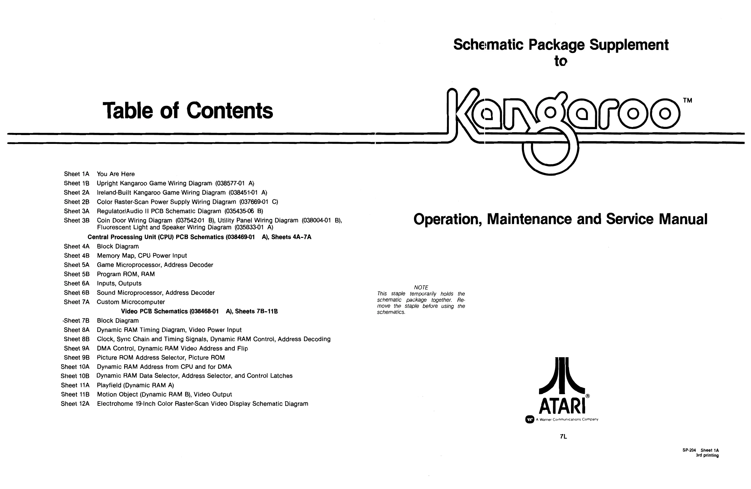
Schematic Package Supplement to
Table of Contents | KG Roe.
Sheet 1B Upright Kangaroo Game Wiring Diagram (038577-01 A) Sheet 2A __Ireland-Built Kangaroo Game Wiring Diagram (038451-01 A) Sheet 2B Color Raster-Scan Power Supply Wiring Diagram (037669-01 C) Sheet 3A Regulator/Audio Il PCB Schematic Diagram (035435-06 B) Sheet 3B Coin Door Wiring Diagram (037542-01 B), Utility Panel Wiring Diagram (038004-01 B), Operation, Maintenance and Service Manual Fluorescent Light and Speaker Wiring Diagram (035833-01 A) Central Processing Unit (CPU) PCB Schematics (038469-01 A), Sheets 4A-7A Sheet 4A Block Diagram Sheet 4B Memory Map, CPU Power Input Sheet 5A Game Microprocessor, Address Decoder Sheet 5B Program ROM, RAM Sheet 6A Inputs, Outputs
7L
‘SP-204 Sheet 1A ard printing
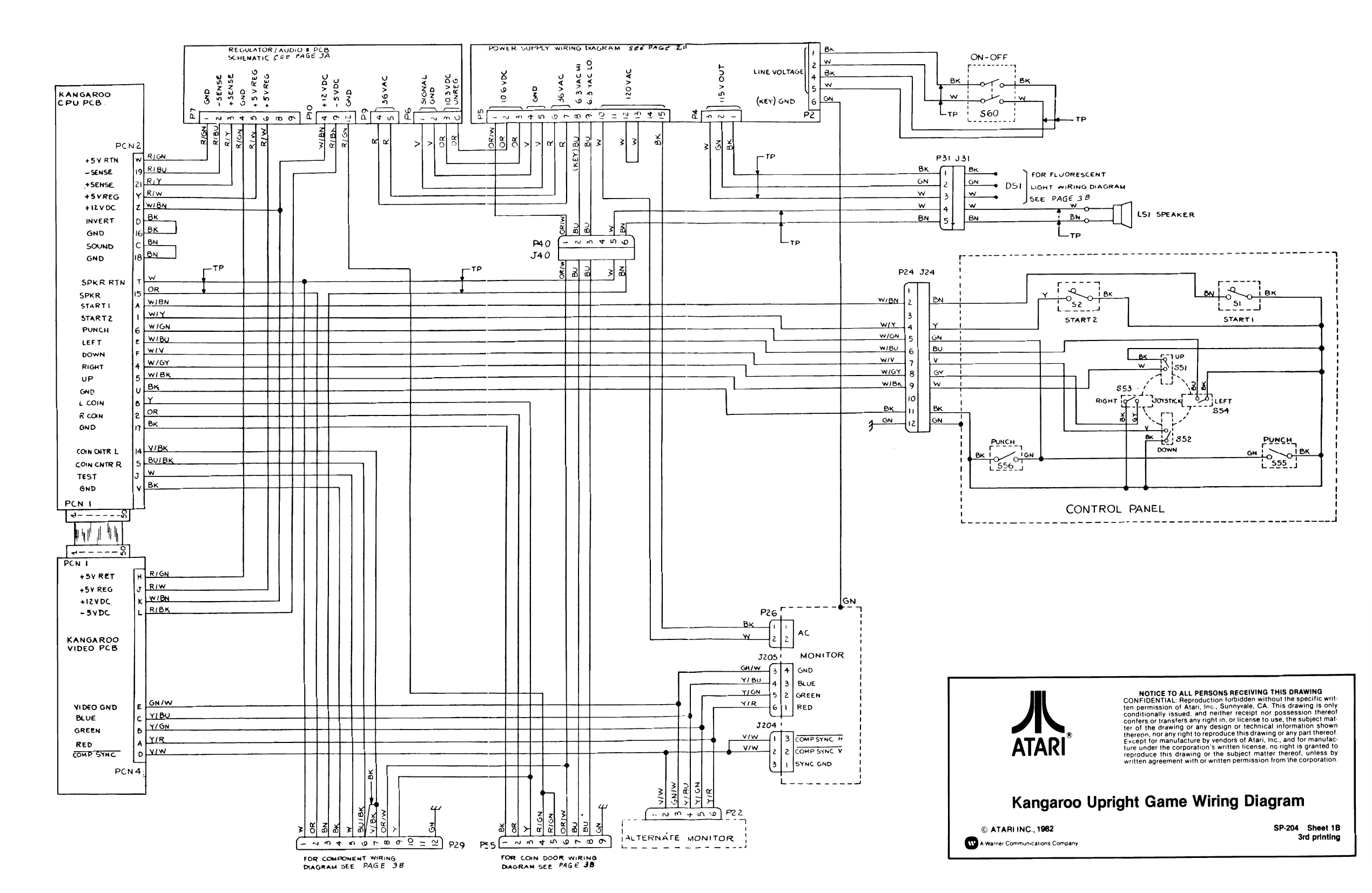
This page is a drawing, shown as the original scan.
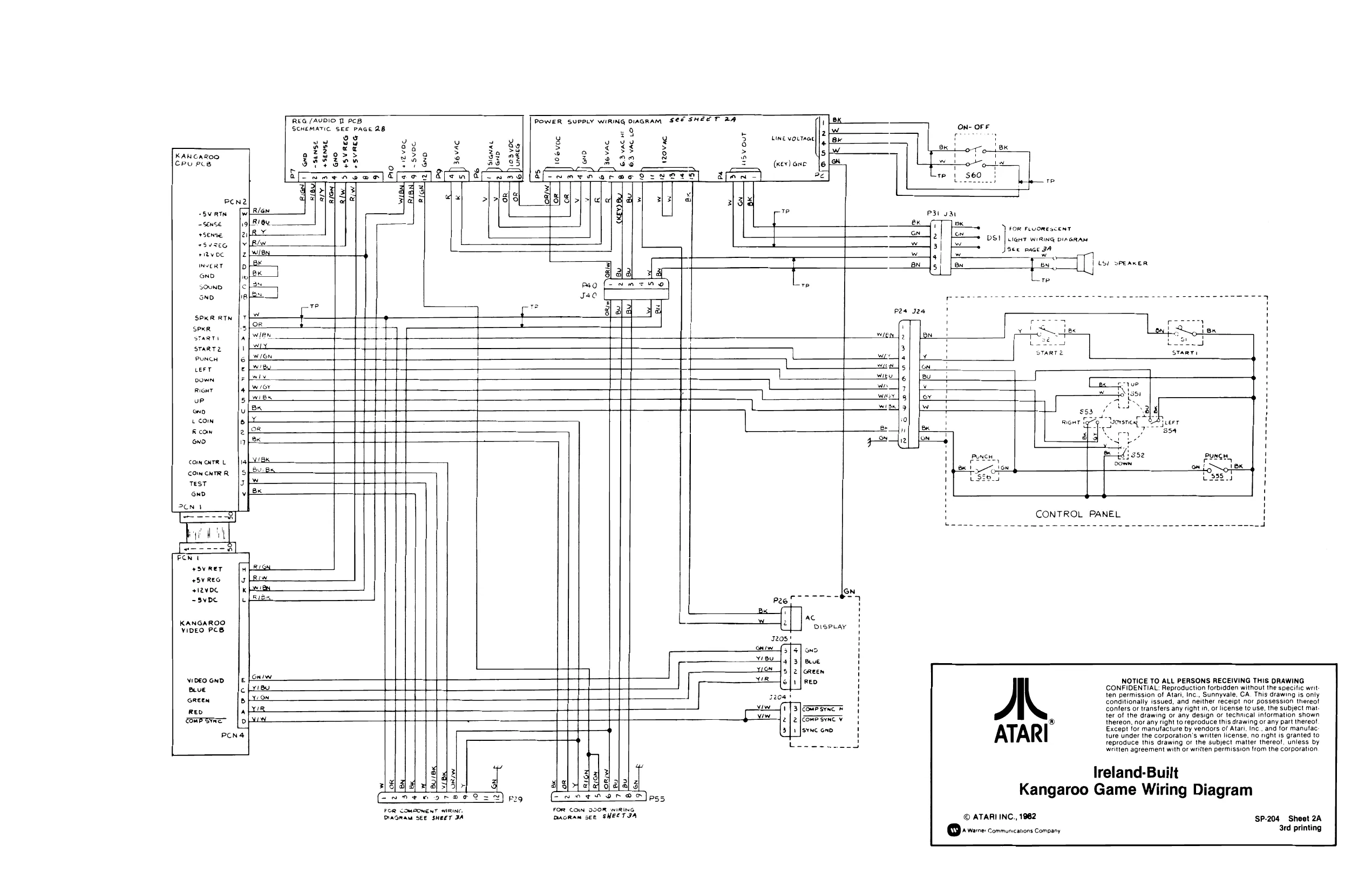
This page is a drawing, shown as the original scan.
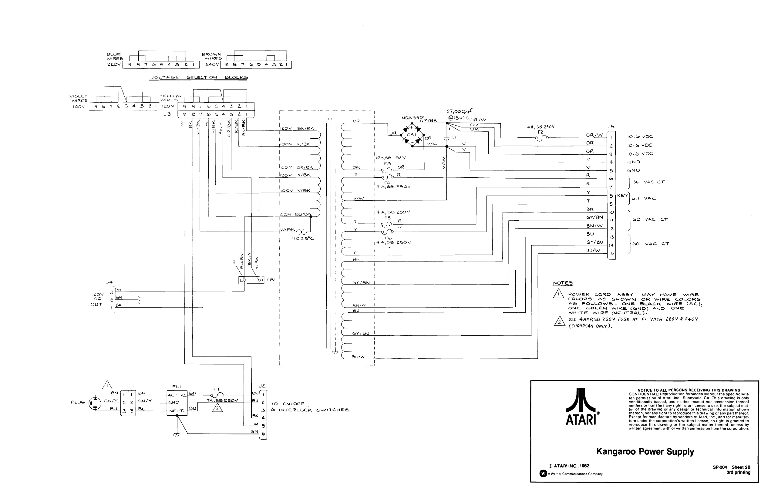
This page is a drawing, shown as the original scan.
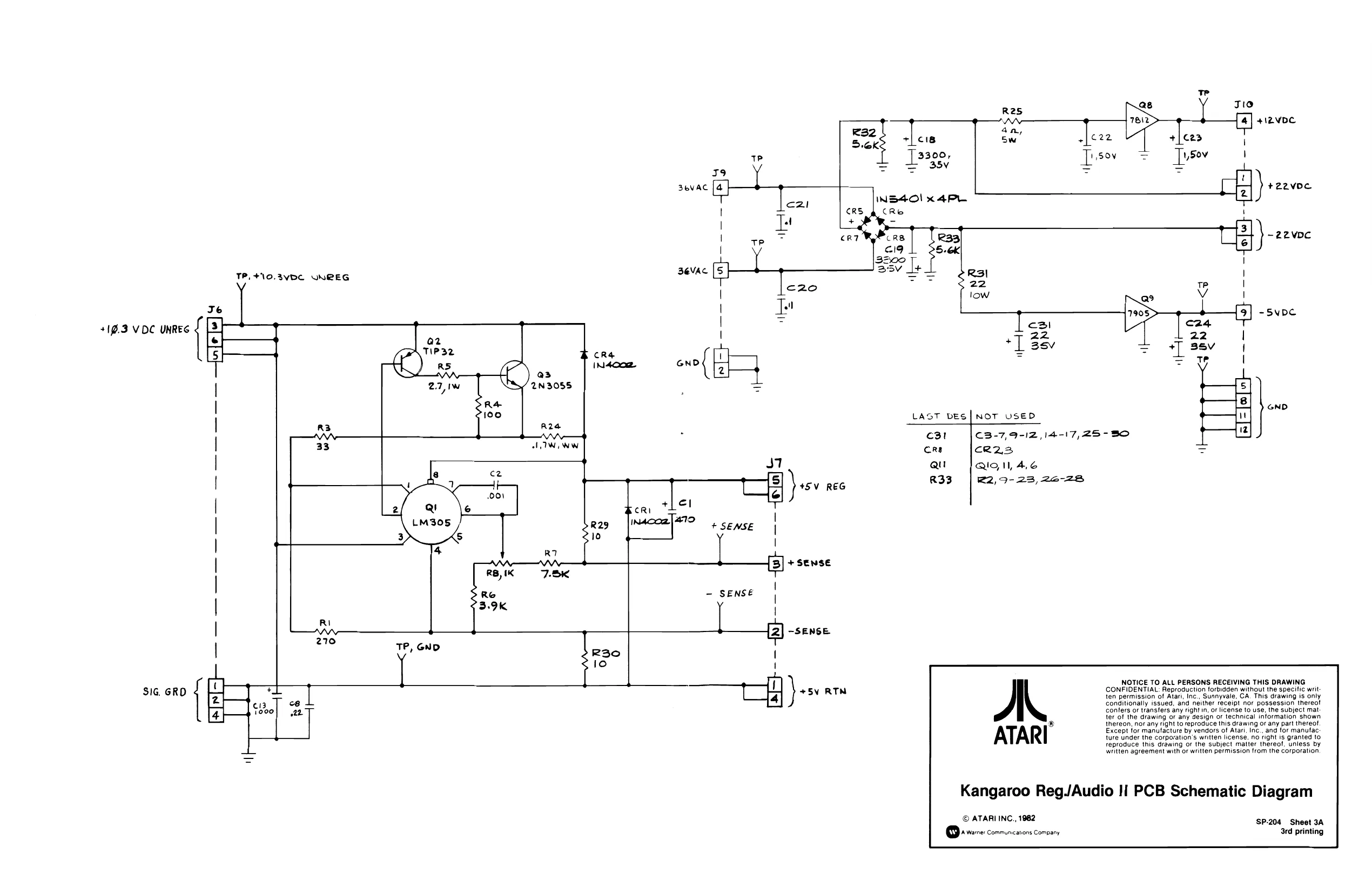
+193 VDC UNRES
SIG. GRD TP, +10.3vDC UNREG
Q2 (Cy ne
- RS ©
RA Qa 2N3058 CRE (N400g 3eVAc
SGVAC
+ SENSE R2s i
+ SENSE
~SENSE
\ +5V RTN +22V0C
~22vDC
- SVD
[TE LAST DES|NOT USED an c3l C3B-7,9-1Z, 14-17, 25-30 [2] crs cR2ZS = au QIO1, AG R33 22,9-23, 26-28
NOTICE TO ALL PERSONS RECEIVING THIS DRAWING CONFIDENTIAL: Reproduction forbidden without the specific writ: ten permission of Atari, Inc., Sunnyvale, CA. This drawing is only conditionally issued, and neither receipt nor possession thereof confers or transters any right in, or license to use, the subject mat. ter of the drawing or any design oF technical information shown ® thereon, nor any right to reproduce this drawing or any part thereot Except for manutacture by vendors of Atari, Inc. and for manufac: ture under the corporation's written license, no right is granted to reproduce this drawing or the subject matter thereof, unless by written agreement with or written permission from the corporation.
Kangaroo Reg/Audio II PCB Schematic Diagram
© ATARI INC., 1982 SP.204 Sheet 3A o- Wamer Communications Company 3rd printing
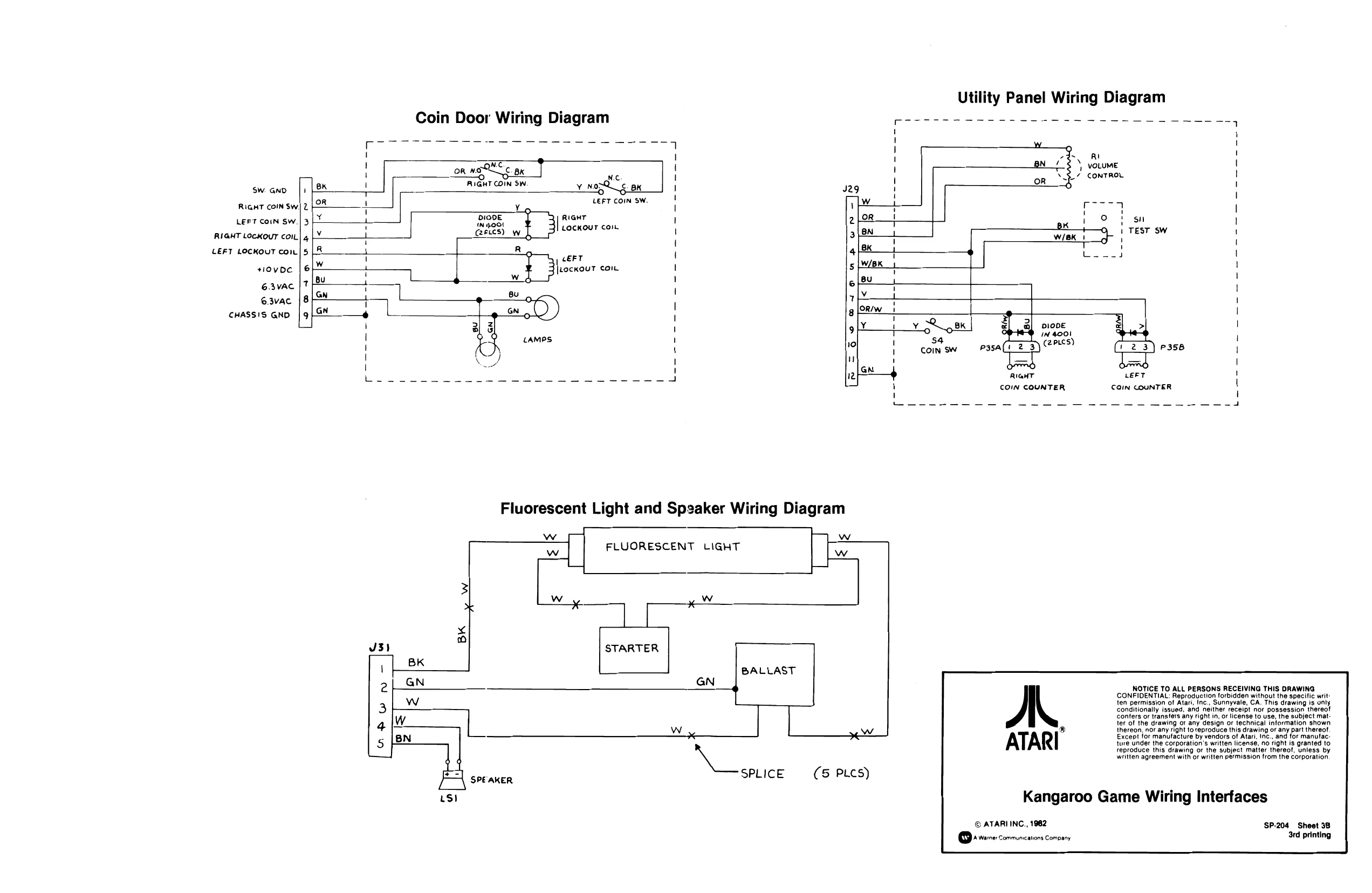
This page is a drawing, shown as the original scan.
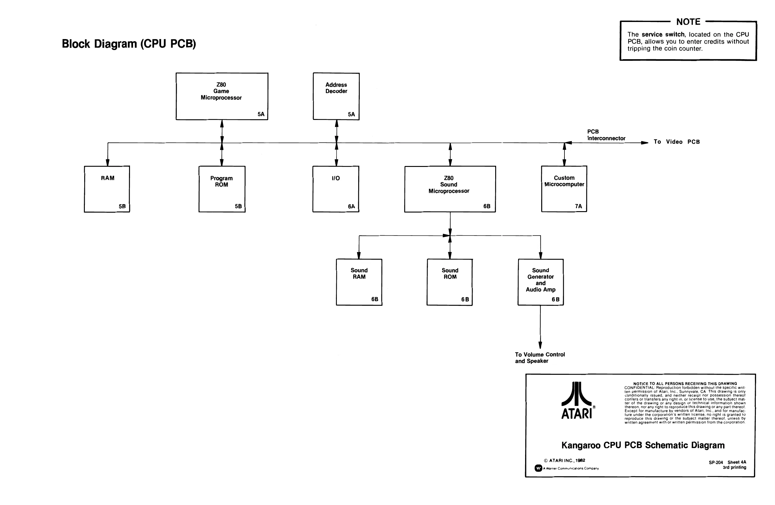
Block Diagram (CPU PCB)
Z80 Game Microprocessor
NOTE
The service switch, located on the CPU PCB, allows you to enter credits without tripping the coin counter.
PCB interconnector
Sound Microprocessor w= To Video PCB
Custom Microcomputer
7A
Sound RAM Sound Generator and Audio Amp
6B
To Volume Control and Speaker
NOTICE TO ALL PERSONS RECEIVING THIS DRAWING CONFIDENTIAL: Reproduction forbidden without the specific wrt ten permission of Atari, Inc., Sunnyvale, CA. This drawing is only canditionally issued, and neither receipt nor possession thereof conlers or transfers any right in, or license to use, the subject matter of the drawing or any design oF technical information shown ® thereon, nor any right to reproduce this drawing or any part thereof, Except for manufacture by vendors of Atari, Inc., and for manufac: ture under the corporation's written license, no right is granted to reproduce this drawing or the subject matier thereof, unless by written agreement with or written permission from the corporation
Kangaroo CPU PCB Schematic Diagram
© ATARI INC., 1982 SP-204 Sheet 4A QA Warr: Communications Company ard printing
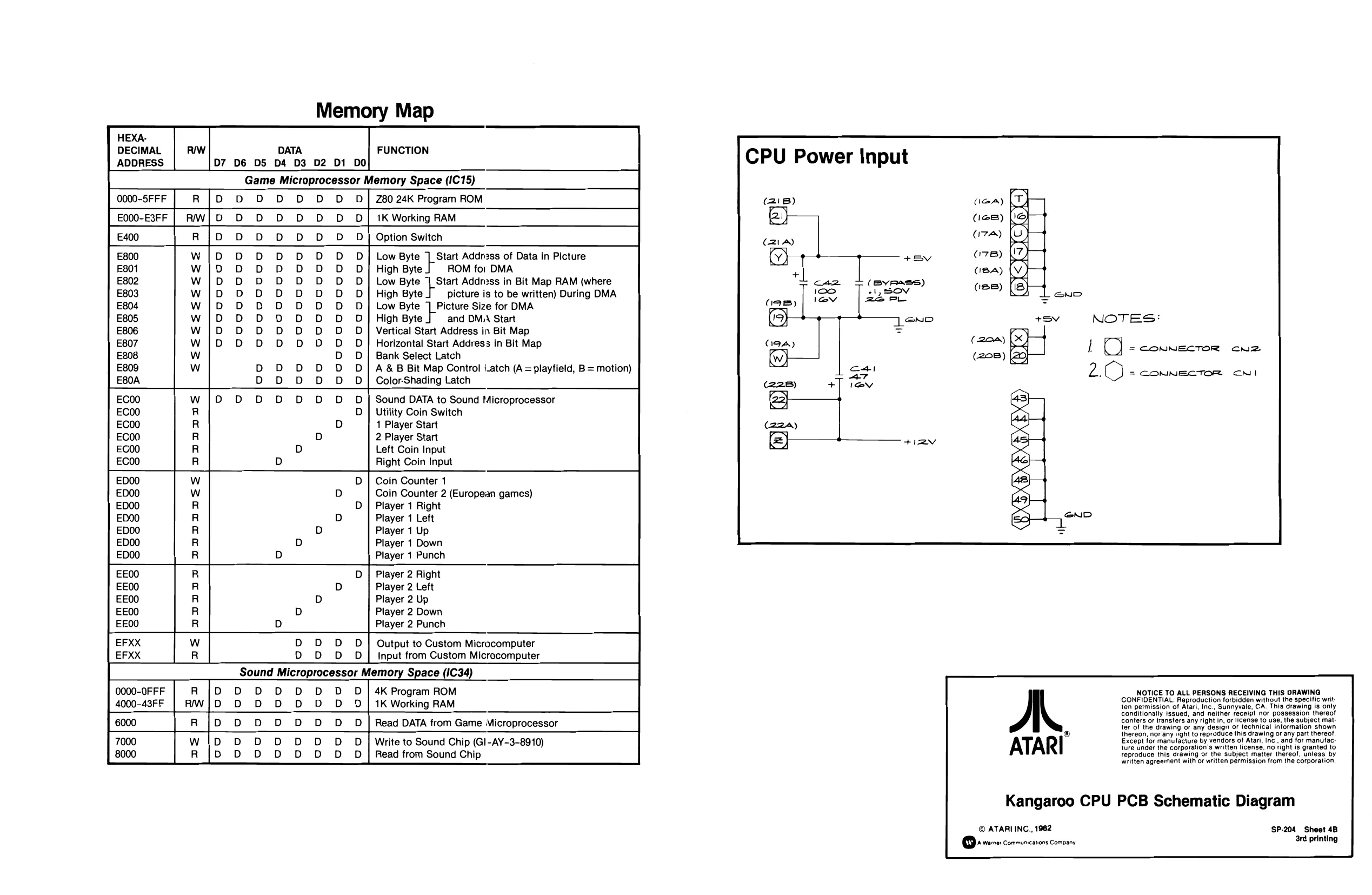
Memory Map
D6 _D5 o1 b3 b2 D1 DO FUNCTION CPU Power Input
Game Microprocessor Memory Space (IC15) 80 24K Program ROM (21B)
1K Working RAM
Option Switch E000-E3FF
Low Byte Start Addrass of Data in Picture High Byte ROM for DMA Low Byte ‘| Start Address in Bit Map RAM (where High Byte picture is to be written) During DMA Low Byte |] Picture Size for DMA High Byte and DMA Start Vertical Start Address in Bit Map Horizontal Start Address in Bit Map CONNECTOR cuz Bank Select Latch )} ; A & B Bit Map Control |_atch (A = playfield, B = motion) Color-Shading Latch : CONNECTOR CN
Sound DATA to Sound Microprocessor Utility Coin Switch 1 Player Start 2 Player Start Left Coin Input Right Coin Input voo000000|o0/oJ/o vo000000Tc/o/0/o0 so00000D0|o|o SSSSSSSSS=E/z oo 01900 900DTDNDDNOIO!SO 9/00 voVDNDDDDIOIO oj00 vouvuDDDNDD]OIO 0 "9JONVNNDVCVVCOCOCOO!O!]O vojo0000000000]oI\0
Coin Counter 1 Coin Counter 2 (European games) Player 1 Right Player 1 Left Player 1 Up Player 1 Down Player 1 Punch
Player 2 Right Player 2 Left Player 2 Up Player 2 Down Player 2 Punch
Output to Custom Microcomputer Input from Custom Microcomputer Sound Microprocessor Memory Space (IC34)
| 0000-0FFF | 4K Program ROM | conNOUige ro ALL PERSONS RECEIVING THIS ORAWING | . |
i leproduction forbidden without the specific writ:
| 4000-43FF | 1K Working RAM | ten permission of Atari, Inc, Sunnyvale, CA. This drawing Is only |
Ww R R R R R
Ww w R R R R R
R R R R R
w R
conditionally issued, and neither receipt nor possession thereof confers or transfers any right in, or license to use, the subject mat- 6000 Read DATA from Game Microprocessor ter of the drawing or any design or technical information shown thereon, nor any right to reproduce this drawing or any part thereof.
| 7000 | Write to Sound Chip (GI-AY-3-8910) | ATAR I | Except for manufacture by vendors of Atari, Inc., and for manufac: |
; ture under the corporation's written license. no right is granted to
| 8000 | Read from Sound Chip | reproduce this drawing or the subject matter thereof, unless by |
written agreement with or written permission from the corporation.
Kangaroo CPU PCB Schematic Diagram
© ATARIING., 1962 SP-204 Sheet 4B |A Warner Communications Company
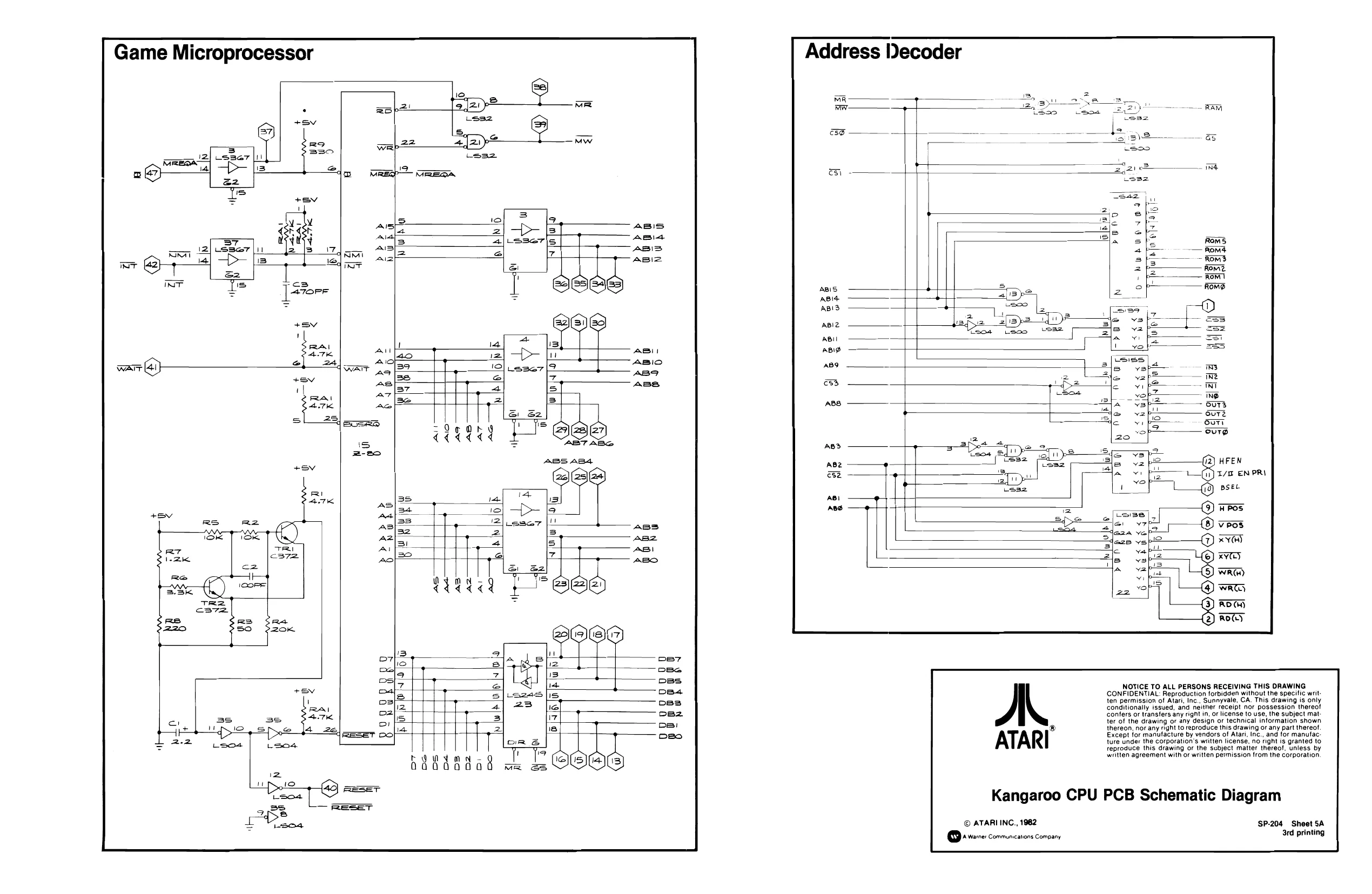
This page is a drawing, shown as the original scan.
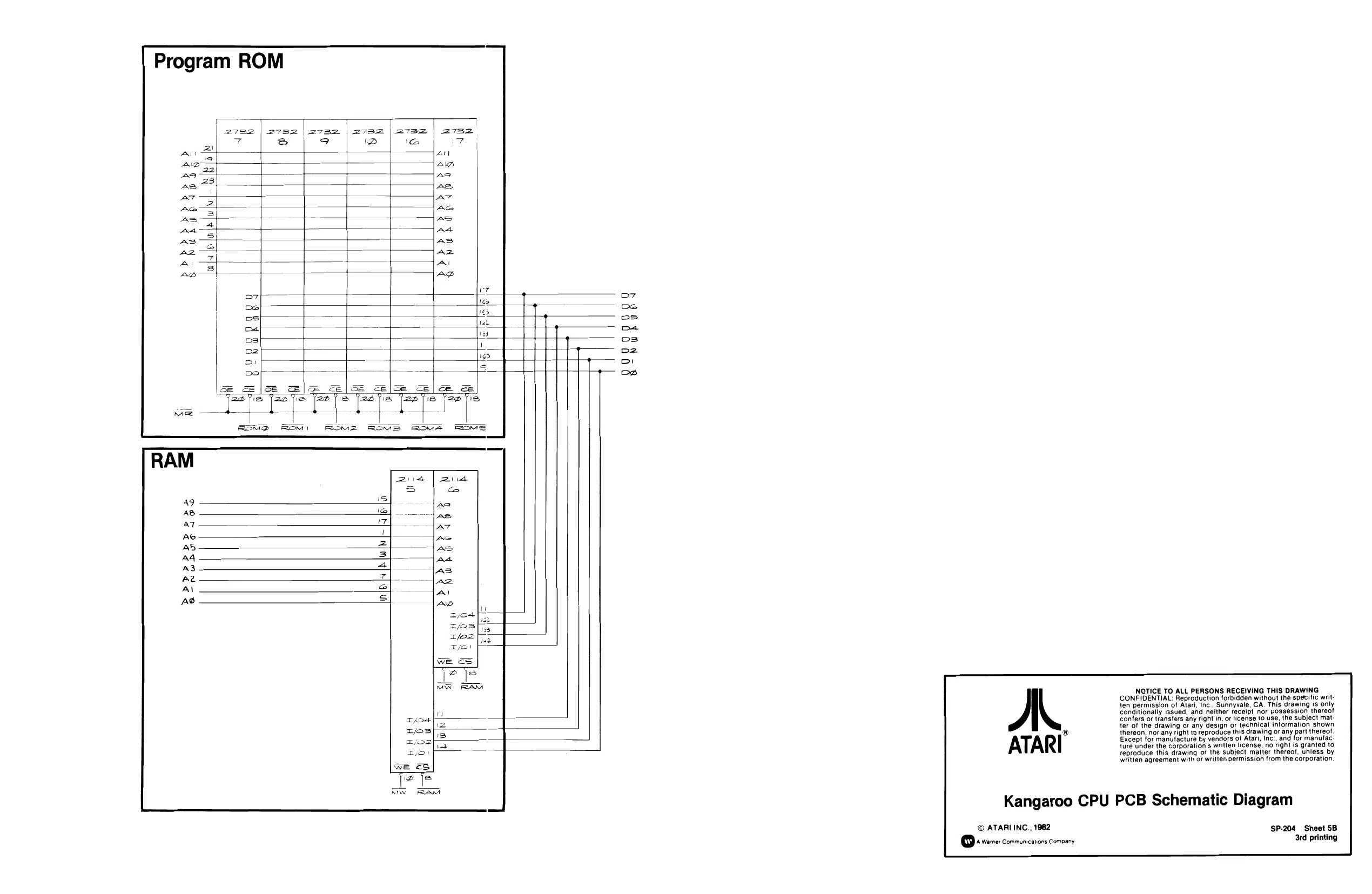
This page is a drawing, shown as the original scan.
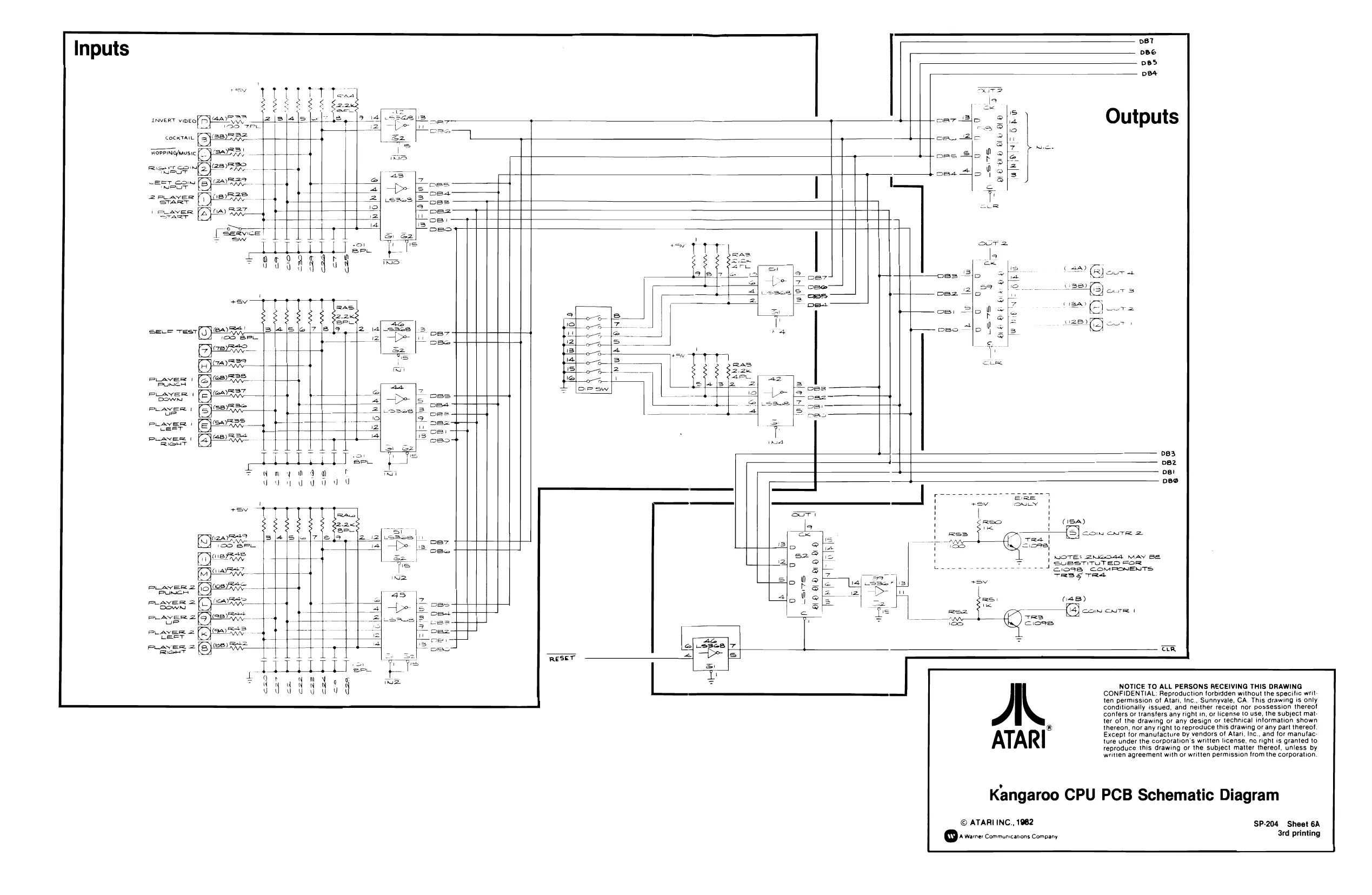
INVERT wibEo|
~=ETLCON
2 PLAYER ae
PLAveR 2 BONEN Payer Baan
PLAvERZ ve Player 2 feet
Puayes= Rat aarRe
say232 es ej) oR! |
jenrese 1) (eye Baste
anR2e fi Ae (Aj Bez
jo} ee RA — +
Reto LRA 4 Gjeean + t ante (} (eo) RS im ui eter v ONO L__
mOCaLS
RESET oss ose oR [ofv
Q it fy
BIH HD 10H DO
Re!
Te, 21698 | COMmONENTS Sasg ret TE: 2Neosd MAY Be BSTITUTED KOR,
48) (Bleamenre
A
ATARI
NOTICE TO ALL PERSONS RECEIVING THIS DRAWING CONFIDENTIAL: Reproduction forbidden without the specific writ ten permission of Atari, Inc., Sunnyvale, CA. This drawing is only conditionally issued, and neither receipt nor possession thereof confers or transfers any right in, or license 10 use, the subject mat: ter of the drawing or any design or technical information shown thereon, nor any right to reproduce this drawing or any part thereof, Except for manufacture by vendors of Atari, Inc., and for manufac. ture under the corporation's written license, no right is granted to reproduce this drawing or the subject matter thereof, unless by written agreement with or written permission from the corporation.
Kangaroo CPU PCB Schematic Diagram
© ATARI INC., 1982
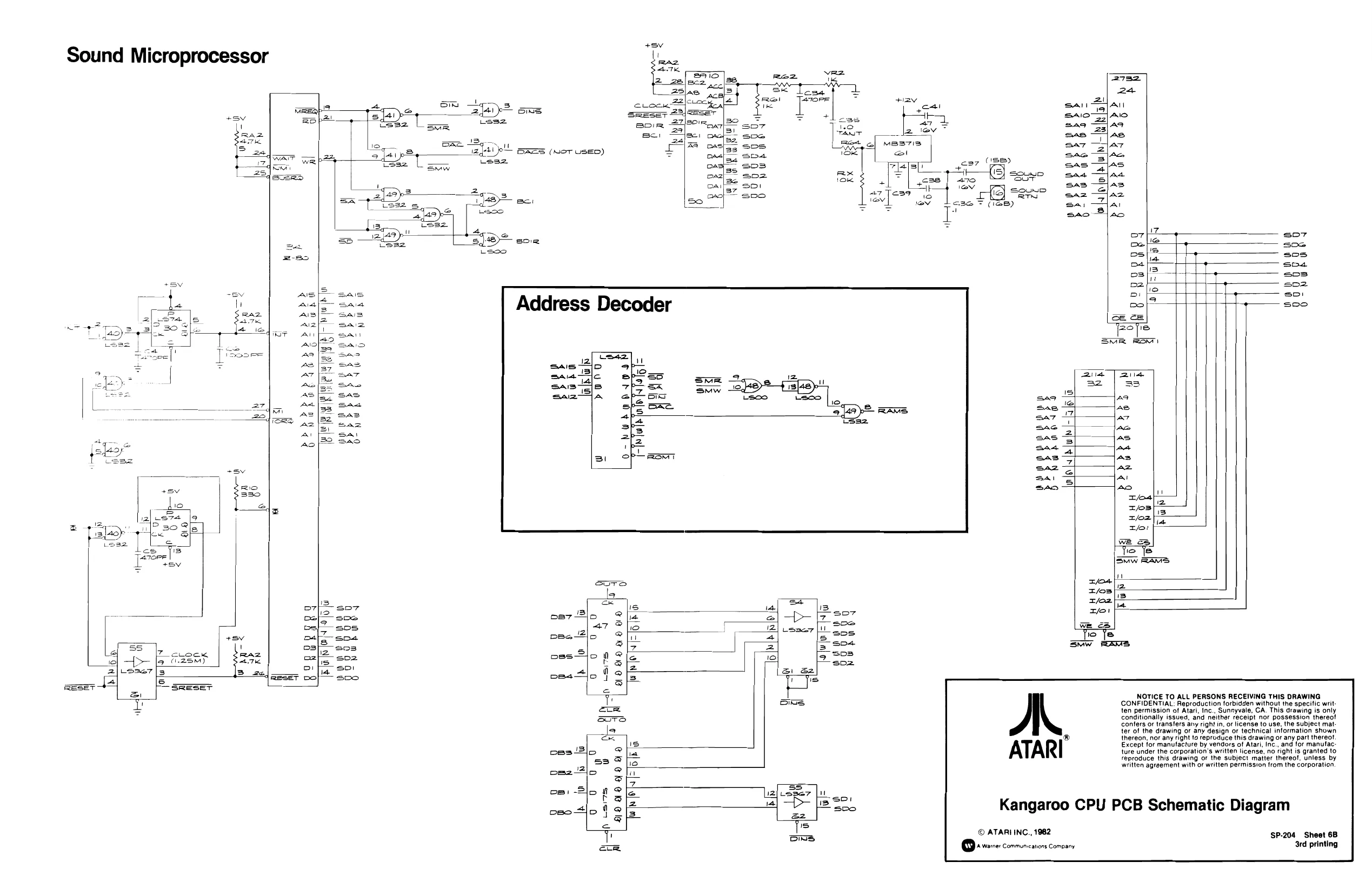
This page is a drawing, shown as the original scan.
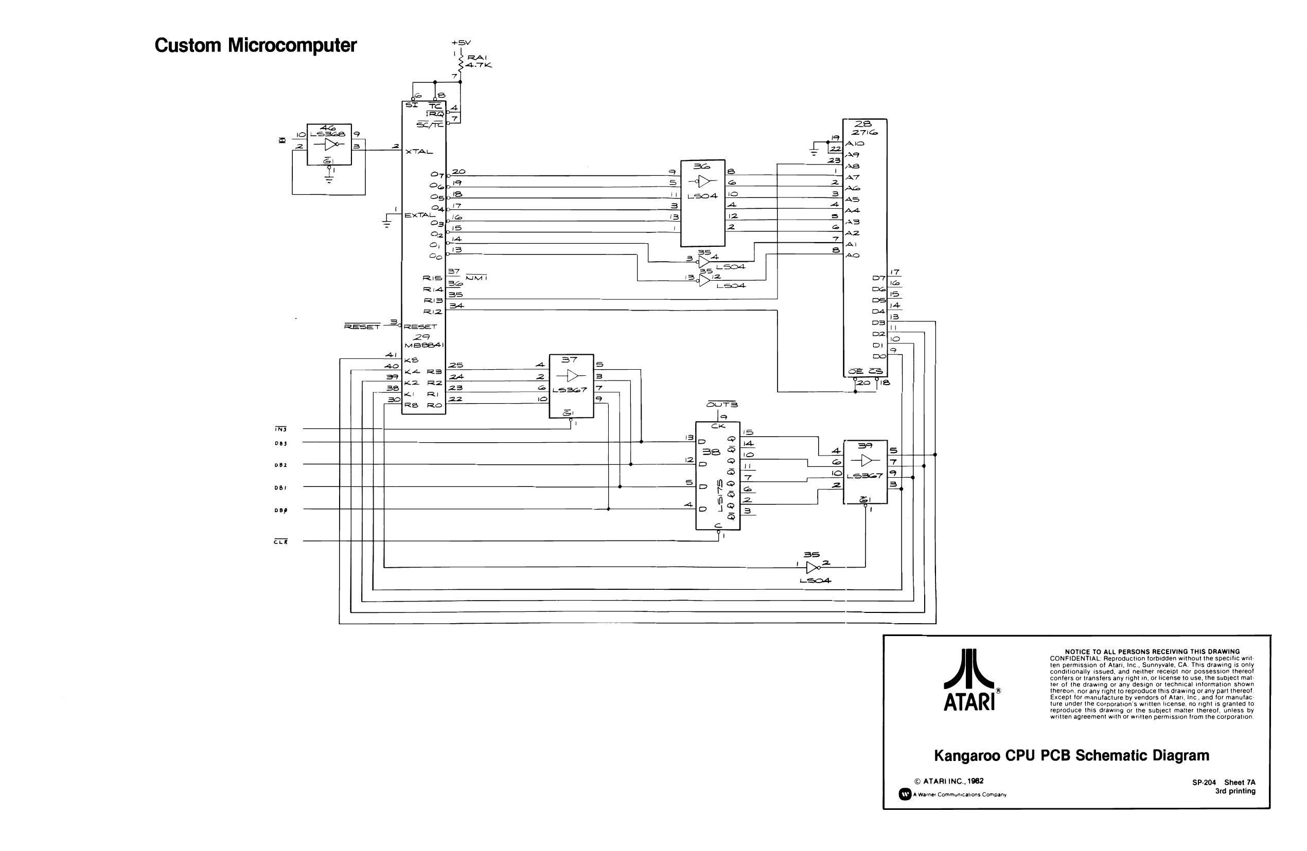
This page is a drawing, shown as the original scan.
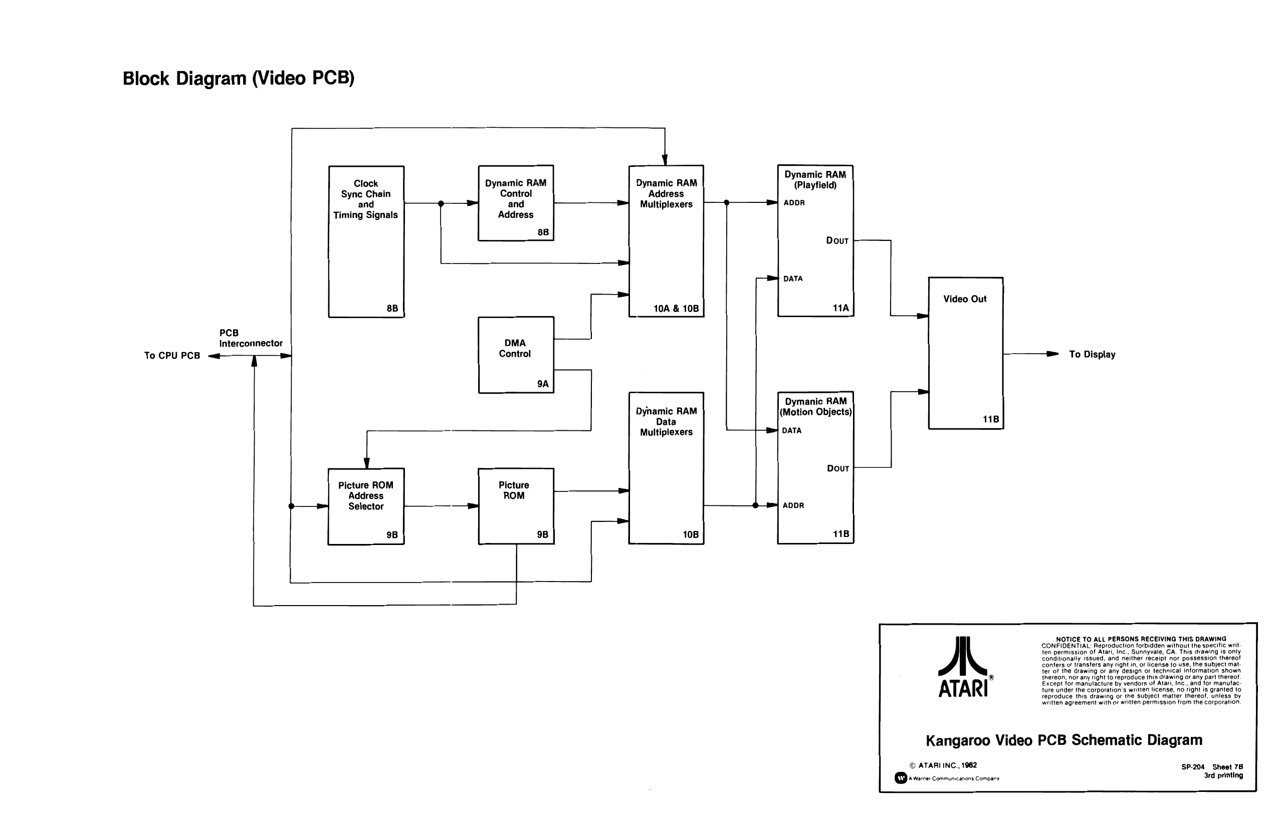
Block Diagram (Video PCB)
PCB Interconnector
To CPU PCB a as
Clock Dynamic RAM Dynamic RAM
Sync Chain Control Address
and and Multiplexers Timing Signals Address
8B
DMA Control
Dynamic RAM Data Multiplexers
Picture ROM Address Selector Picture ROM
9B 10A & 10B Dynamic RAM (Playfield)
ADDR
Dymanic RAM (Motion Objects)|
DATA Video Out
To Display
NOTICE TO ALL PERSONS RECEIVING THIS DRAWING CONFIDENTIAL: Reproduction forbidden without the specific writ ten permission of Atari, Inc., Sunnyvale, CA. This drawing is only conditionally issued, and neither receipt nor possession thereo! confers of transfers any right in, or license to use, the subject matter of the drawing or any design or technical information shown thereon, nor any right to reproduce this drawing or any part thereof. Except for manulacture by vendors of Atari, Inc., and for manufac: ture under the corporation's written license, no right is granted to reproduce this drawing or the subject matter thereof, unless by written agreement with or written permission from the corporation. AL
ATARI
Kangaroo Video PCB Schematic Diagram
© ATARI INC., 1982 SP-204 Sheet 7B
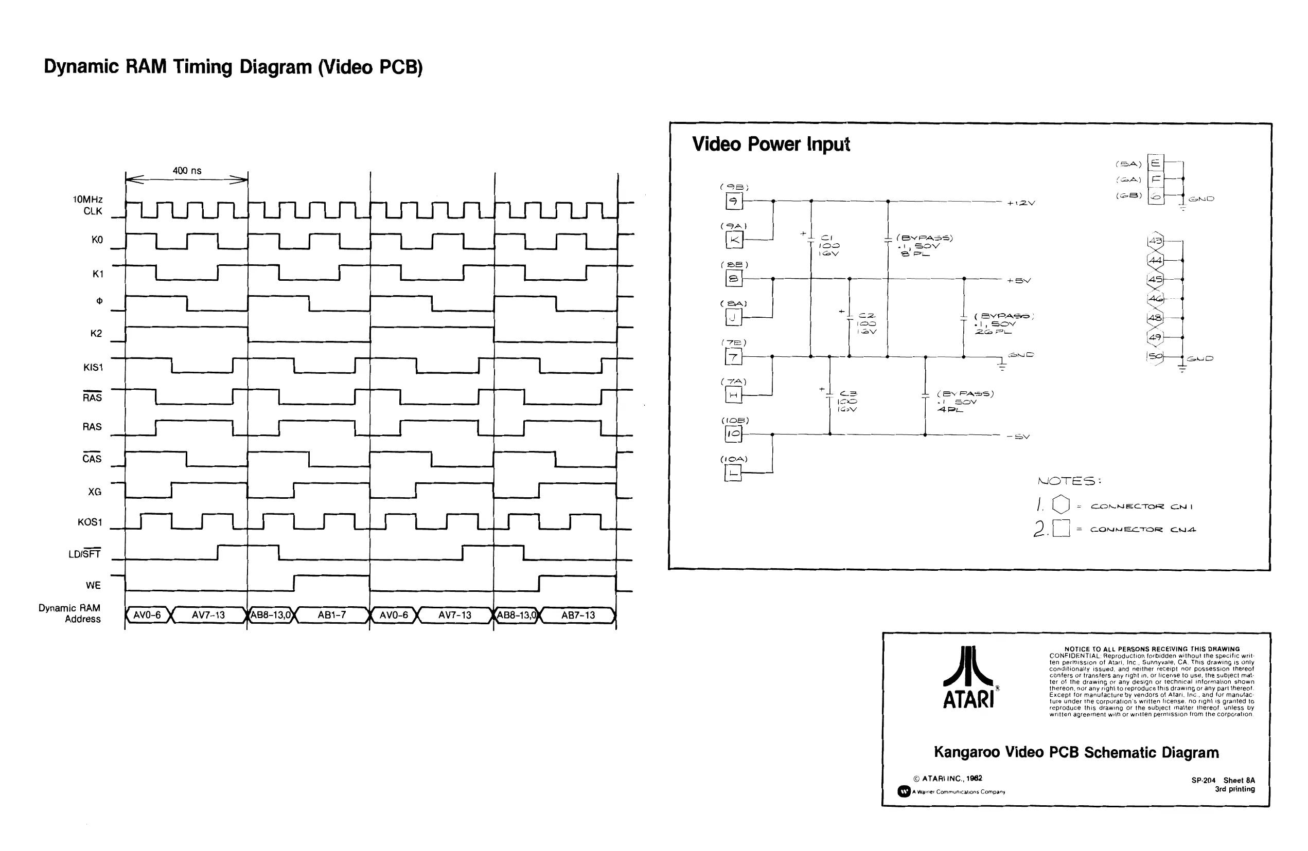
This page is a drawing, shown as the original scan.
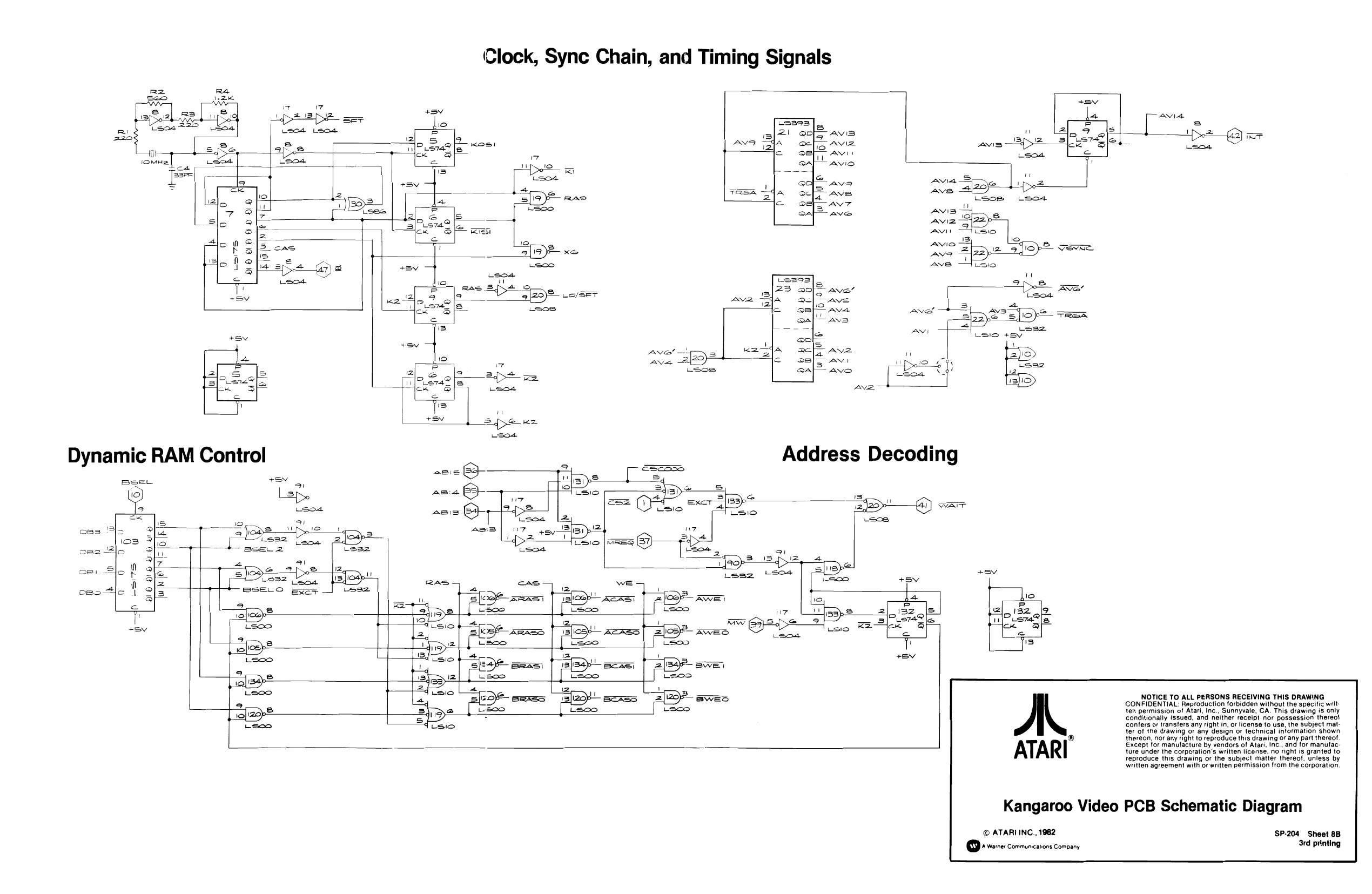
This page is a drawing, shown as the original scan.
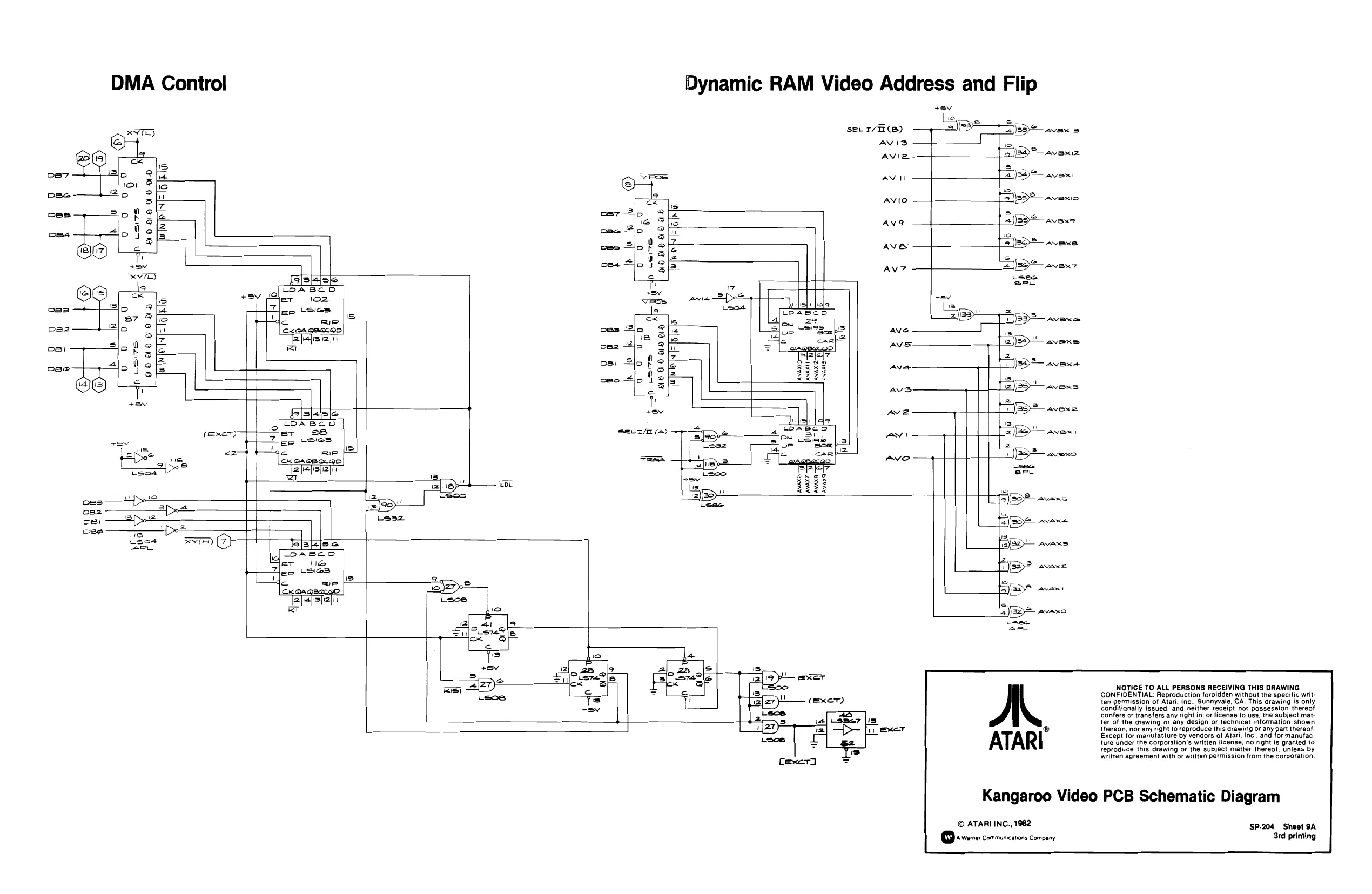
This page is a drawing, shown as the original scan.
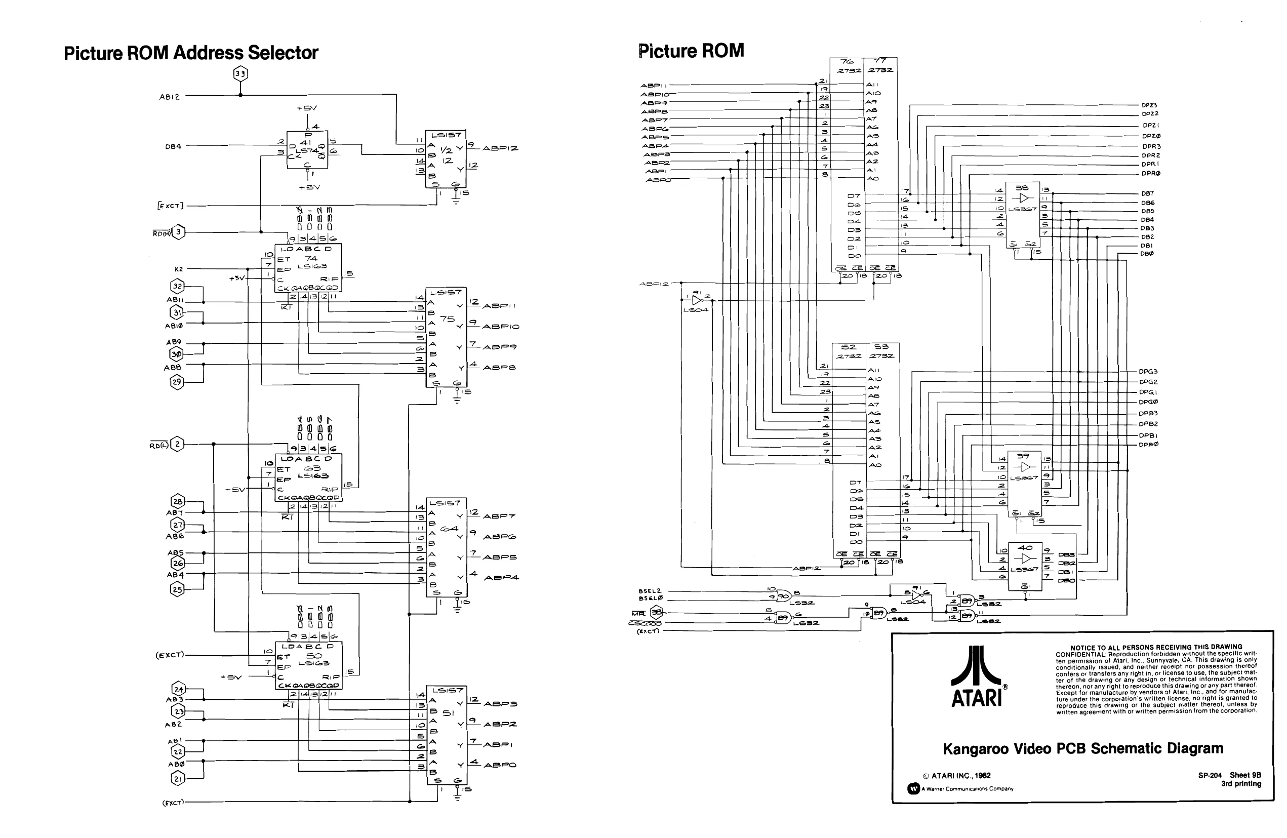
This page is a drawing, shown as the original scan.
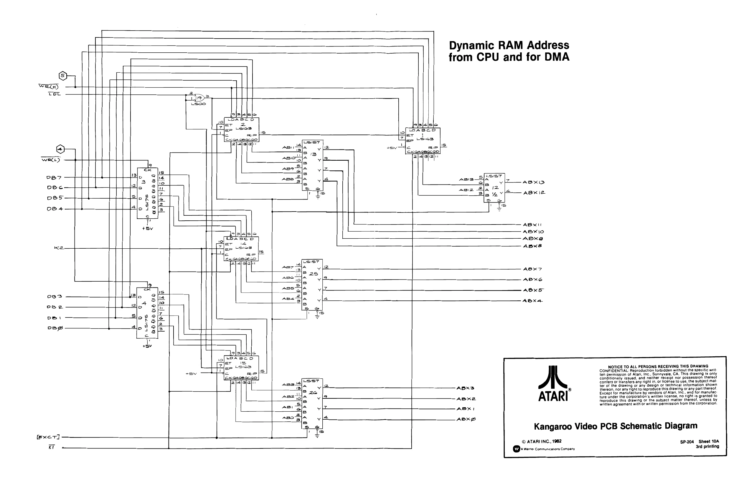
This page is a drawing, shown as the original scan.
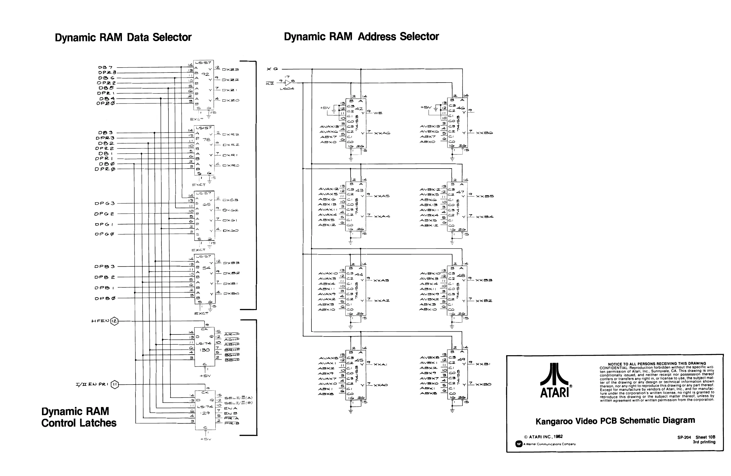
This page is a drawing, shown as the original scan.
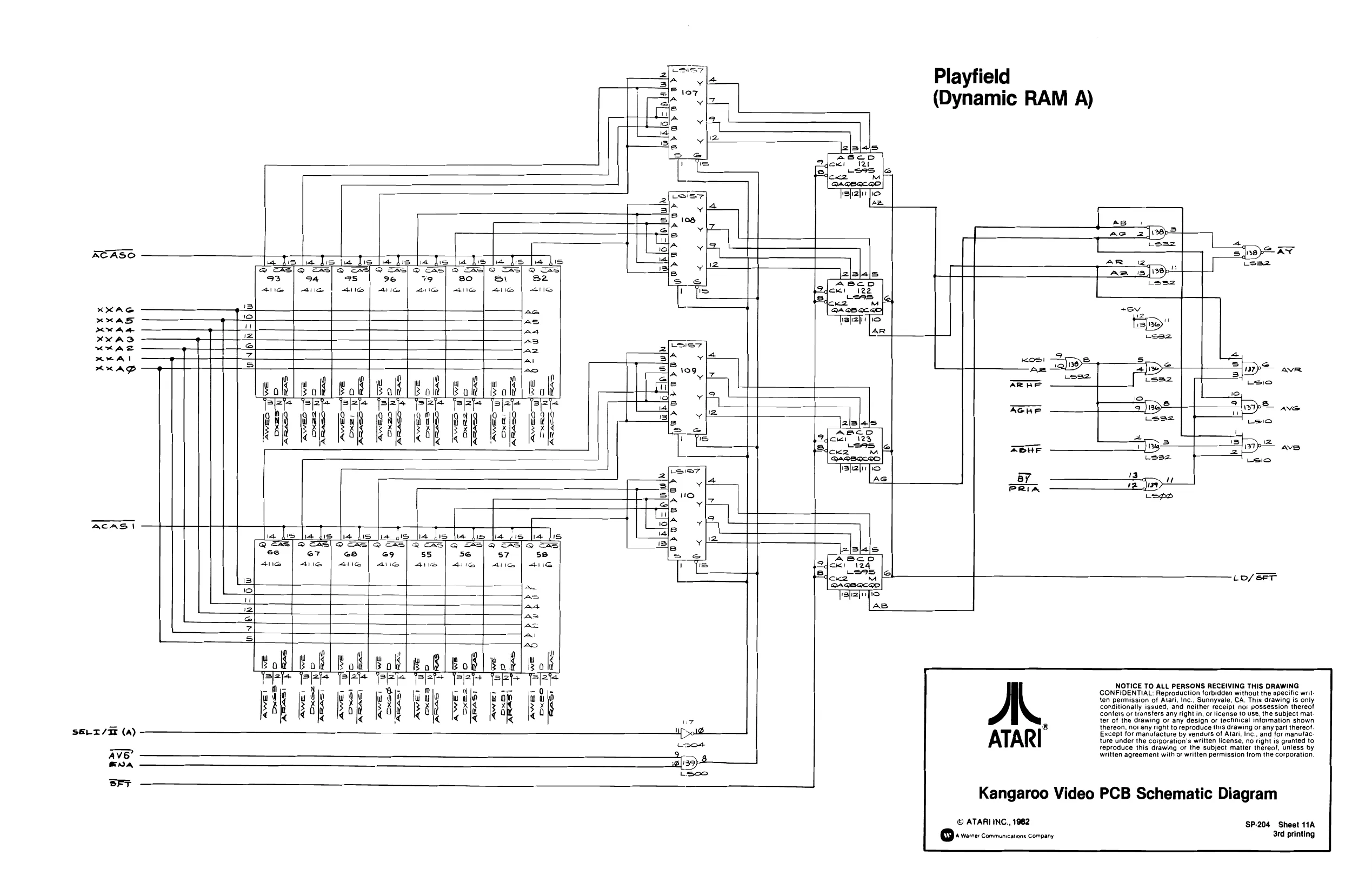
This page is a drawing, shown as the original scan.
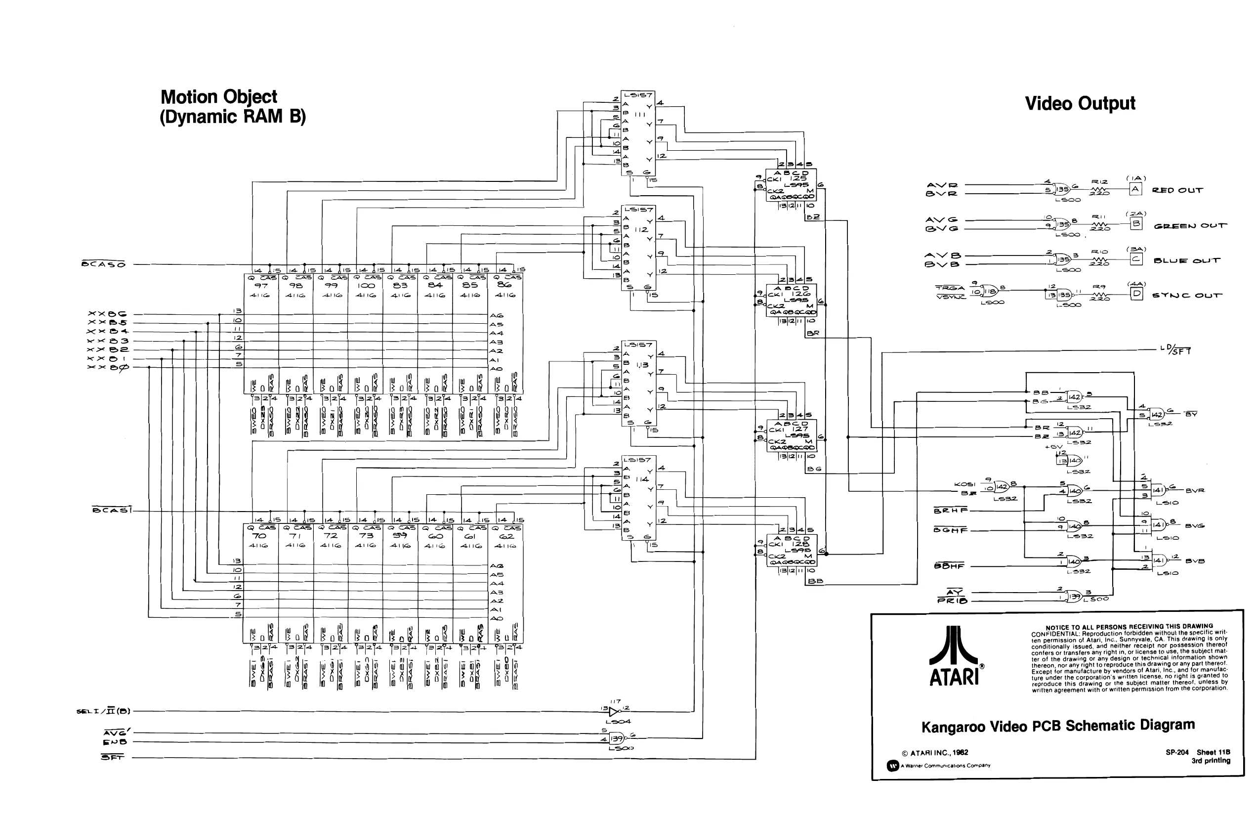
This page is a drawing, shown as the original scan.