Major Havoc SP-252 1st Printing
Major Havoc (rev 3) (Atari, 1983) · Schematic Package · 19 pages · 47 sections · original scan
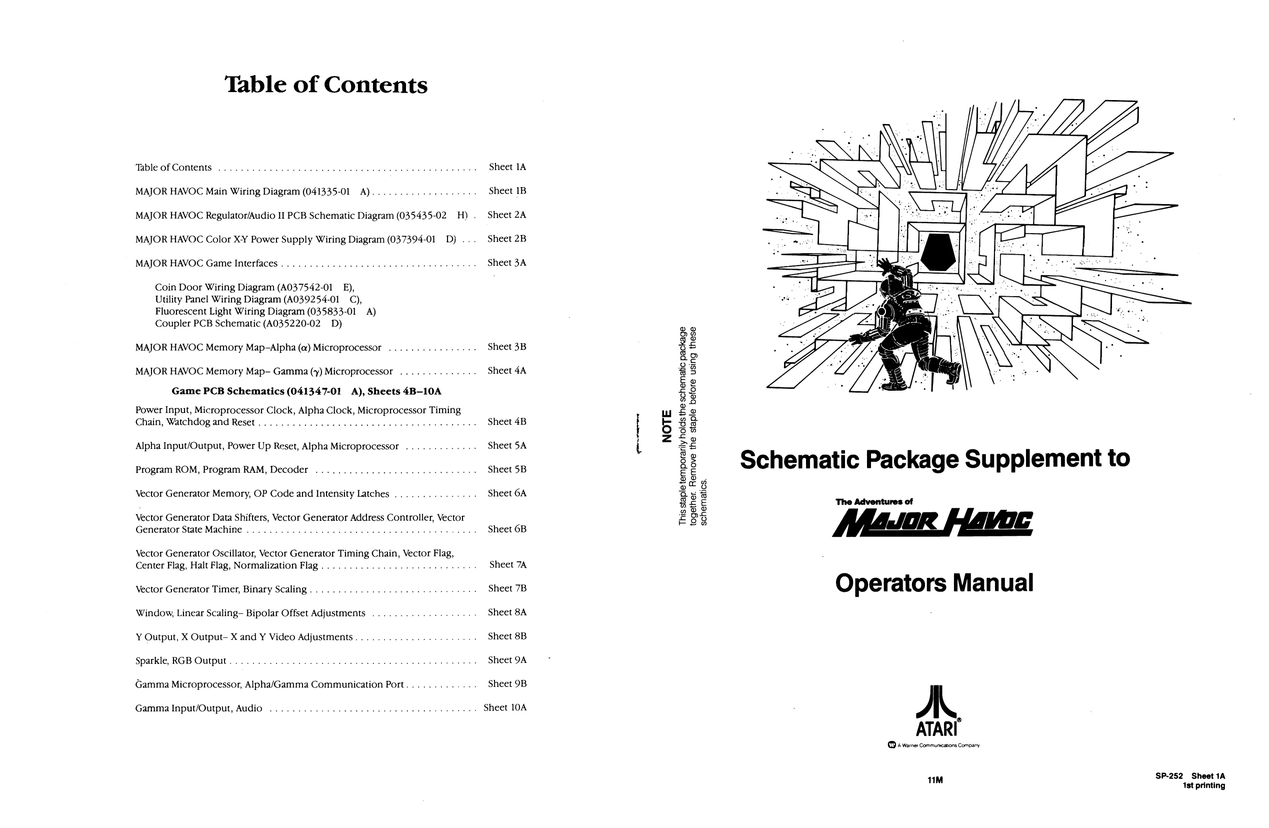
Table of Contents
Table of Contents ................
MAJOR HAVOC Main Wiring Diagram (041335-01 A).............-55
MAJOR HAVOC Regulator/Audio II PCB Schematic Diagram (035435-02 H)
MAJOR HAVOC Color X¥ Power Supply Wiring Diagram (037394-01 D) .
MAJOR HAVOC Game Interfaces .......... F Law eo Lau abe be
Coin Door Wiring Diagram (A037542-01_E), Utility Panel Wiring Diagram (A039254-01_ C), Fluorescent Light Wiring Diagram (035833-01 A) Coupler PCB Schematic (A035220-02 D)
MAJOR HAVOC Memory Map-Alpha (a) Microprocessor ..
MAJOR HAVOC Memory Map- Gamma (y) Microprocessor ...........
Game PCB Schematics (041347-01 A), Sheets 4B-10A
Power Input, Microprocessor Clock, Alpha Clock, Microprocessor Timing Chain, Watchdog and Reset ........... 000 cece cence eee cera
Alpha Input/Output, Power Up Reset, Alpha Microprocessor .......-
Program ROM, Program RAM, Decoder .................-5.
Vector Generator Memory, OP Code and Intensity Latches ...........
Vector Generator Data Shifters, Vector Generator Address Controller, Vector Generator State Machine ............ ee ees
Vector Generator Oscillator, Vector Generator Timing Chain, Vector Flag, Center Flag, Halt Flag, Normalization Flag... . .
Vector Generator Timer, Binary Scaling.............-
Window, Linear Scaling- Bipolar Offset Adjustments
Y Output, X Output- X and Y Video Adjustments
Sparkle, RGB Output...................0220.
Gamma Microprocessor, Alpha/Gamma Communication Port .
Gamma Input/Output, Audio ... 2.2.02... 0600.20 c eee eee eee Sheet 1A
Sheet 1B
Sheet 2A
Sheet 2B
Sheet 3A
Sheet 3B
Sheet 4A
Sheet 4B
Sheet 5A
Sheet 5B
Sheet 6A
Sheet 6B
Sheet 7A
Sheet 7B
Sheet 8A
Sheet 8B
Sheet 9A
Sheet 9B
. Sheet 10A
schematics. Schematic Package Supplement to
The Adventures of Meson Hlavec
Operators Manual
AL ATARI ©) A varerConmurcatons Company
SP-252 Sheet 1A aM 1st printing
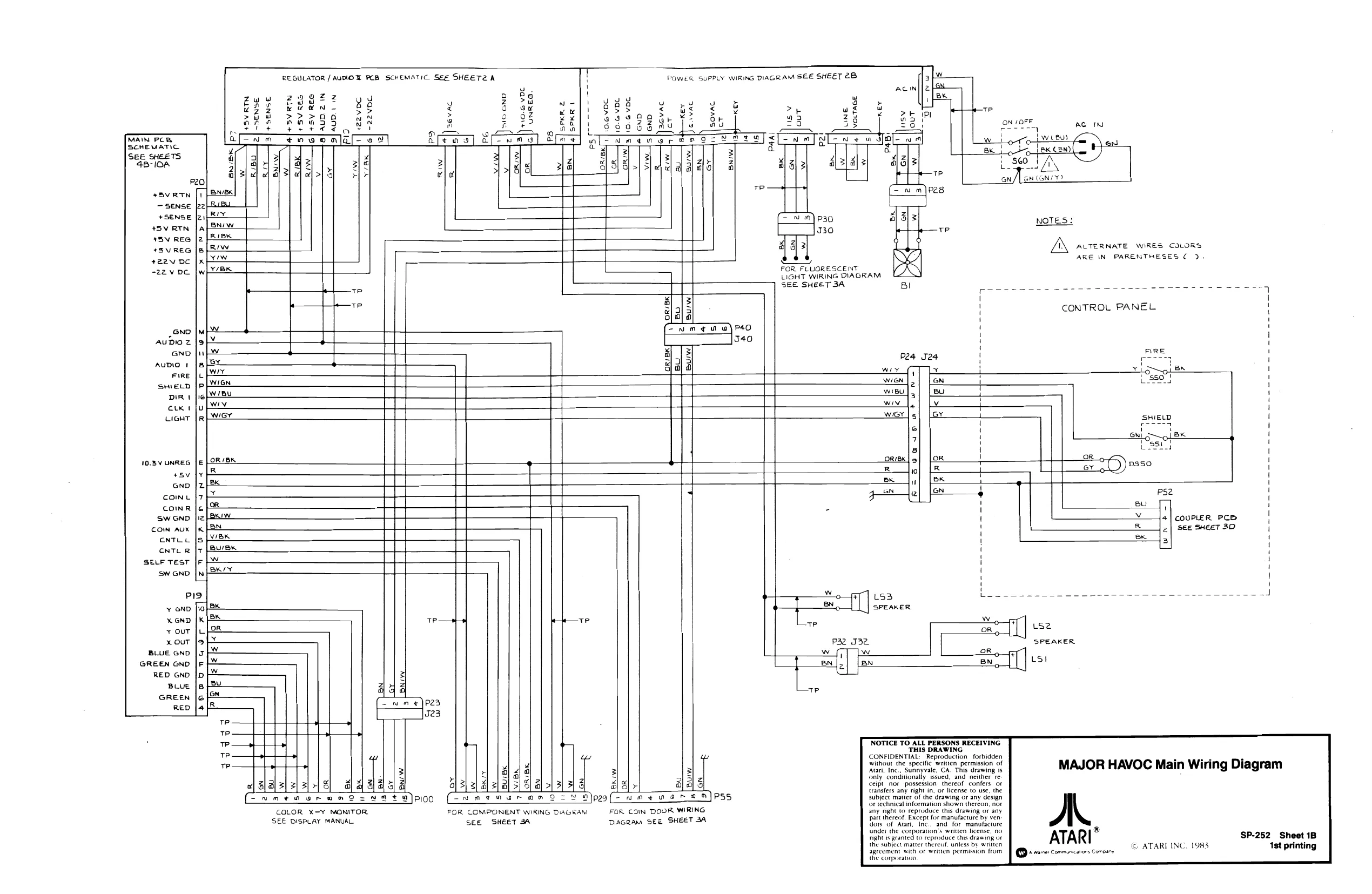
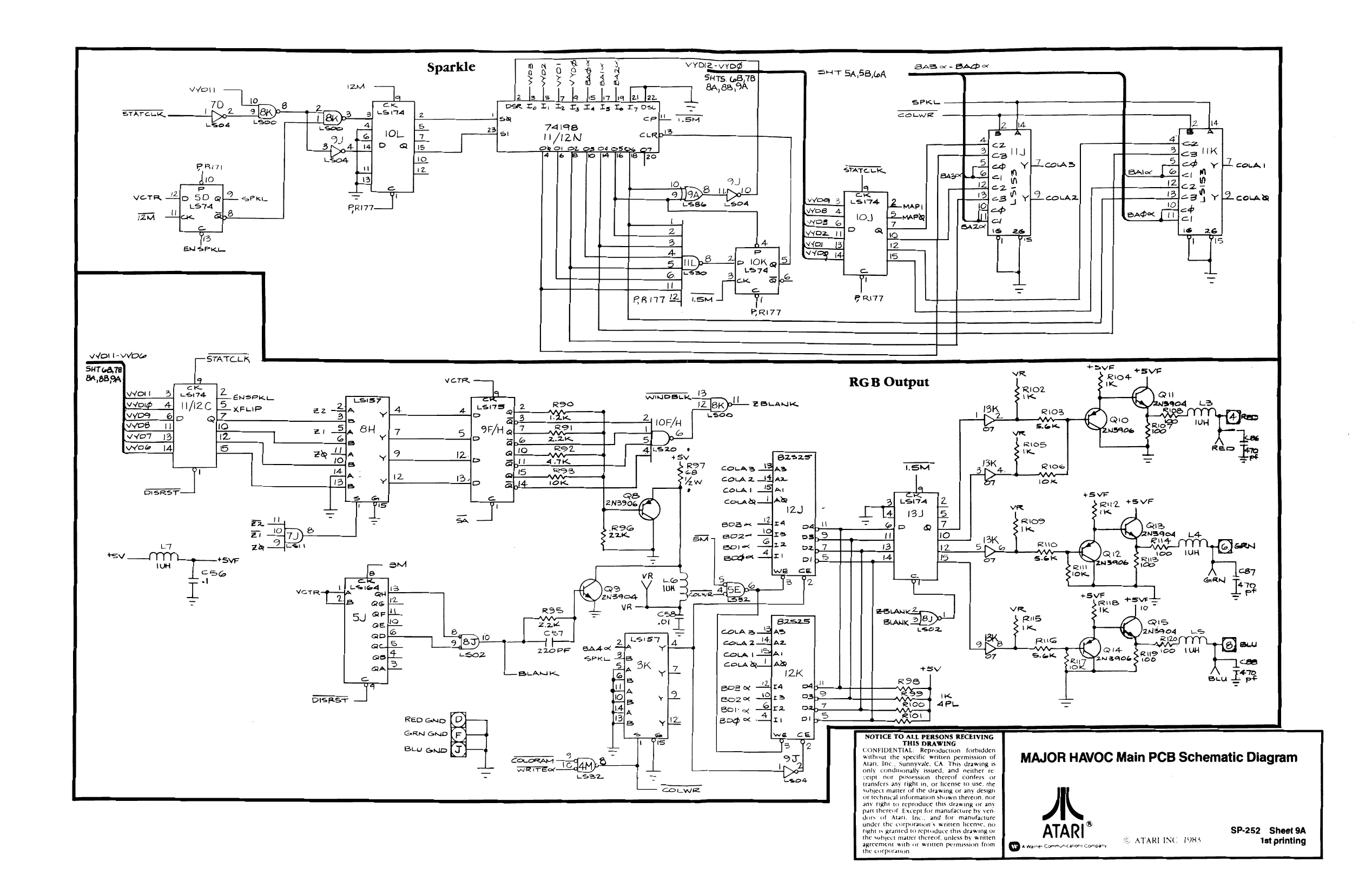
This page is a drawing, shown as the original scan.
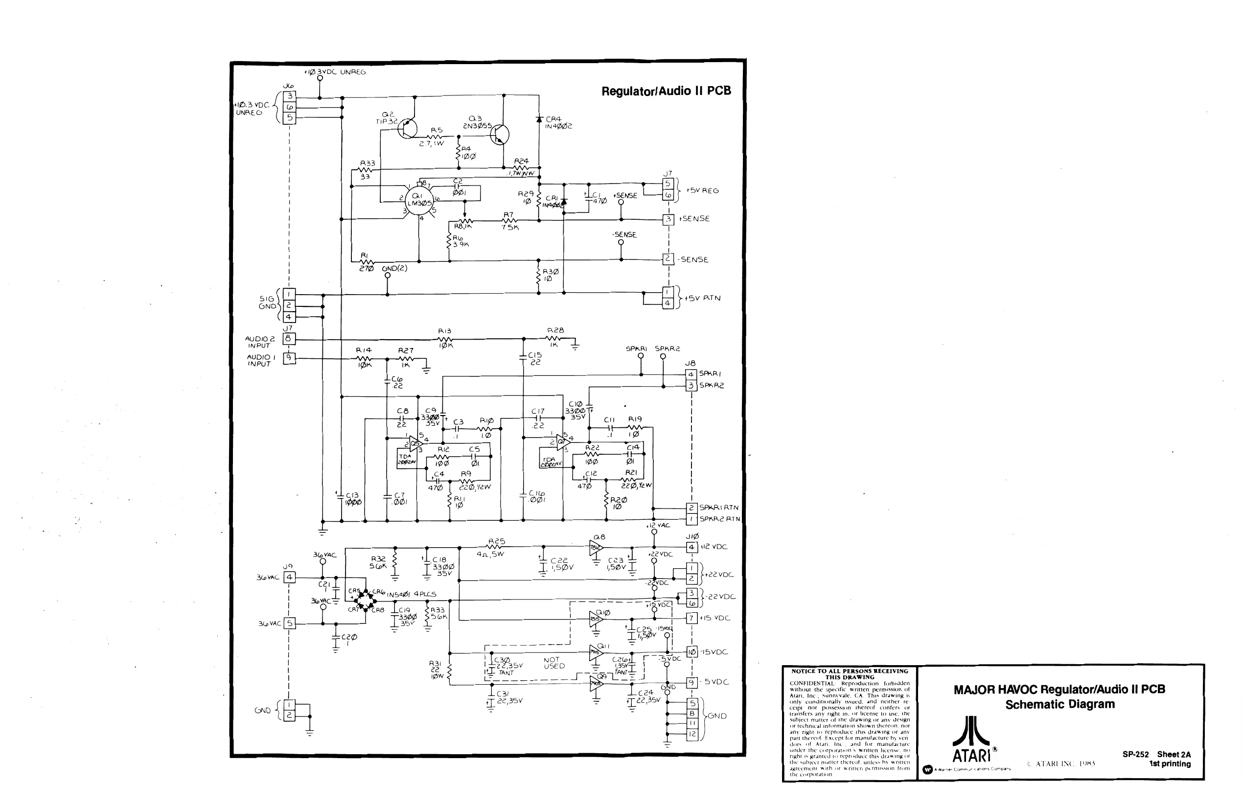
This page is a drawing, shown as the original scan.
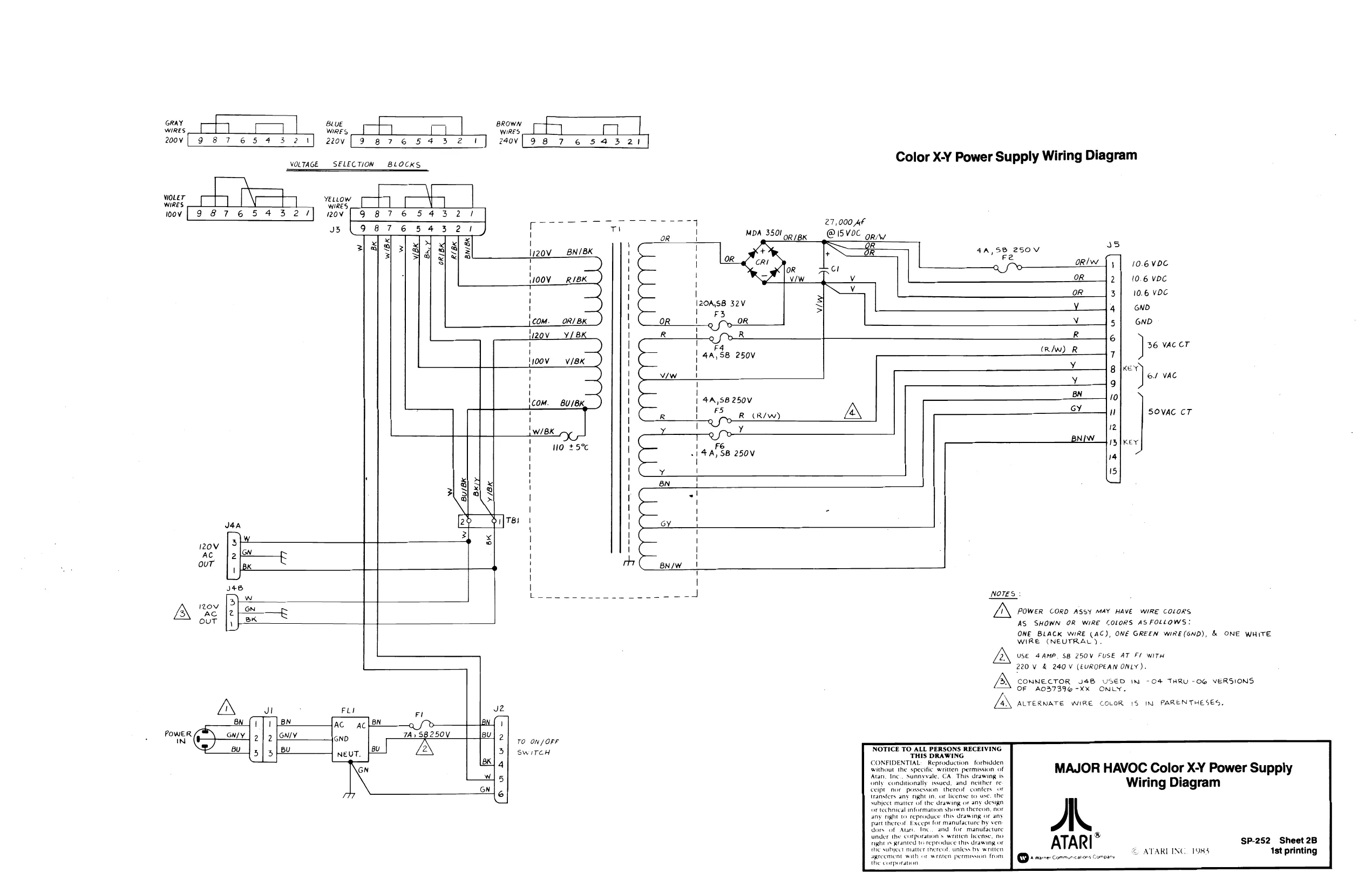
This page is a drawing, shown as the original scan.
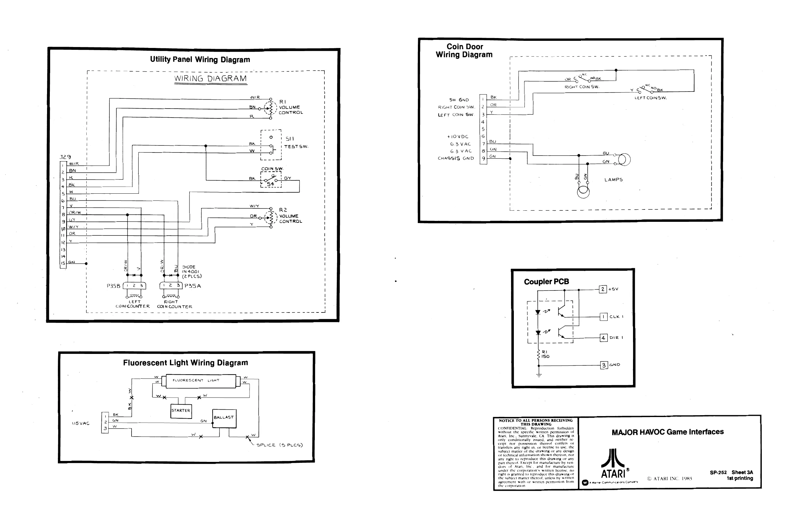
Coin Door
Utility Panel Wiring Diagram Wiring Diagram
WIRING DIAGRAM or CL 108K
7 COINS! x RIGHT COIN SW. 1 oO a
LEFT COINSW. Sw GND BN 5 1y3 | VOLUME RIGHT COIN SW. ep CONTROL LerT COIN SW
| © | isn | +10V0C |
| io, | | TESTSW. | ©3 VAC |
| ; | ot | 63 VAC |
L -—— CHASSIS GND nN Re OewraAnkw A
lo iz COIN Sw. w x
le In
ka
Re VOLUME 5.’ CONTROL,
DIODE IN 4001 (2PLCS)
an Coupler PCB
LEFT RIGHT COINCOUNTER COINCOUNTER,
FLUORESCENT Lian ("
oi
noi ne sree emi aenaiy MAJOR HAVOC Game Interfaces
subject matter of the drawing or any design, Or technical information shown thereon, nor any right to reproduce this drawing or any part thercot. Except for manufacture by ven: dors of Alan, Ine, and for manufacture ader the corporation's witten license, ne ® SP-252 Sheet 3A Fight ty granted to reproduce this drawing ot Seen ATART gs ssantise: wns sprinting agreement with or writen permission from I Qa mane: conmancarons Conary the corporation MIS VAC
aan x we
starter
BALLAST nv
<
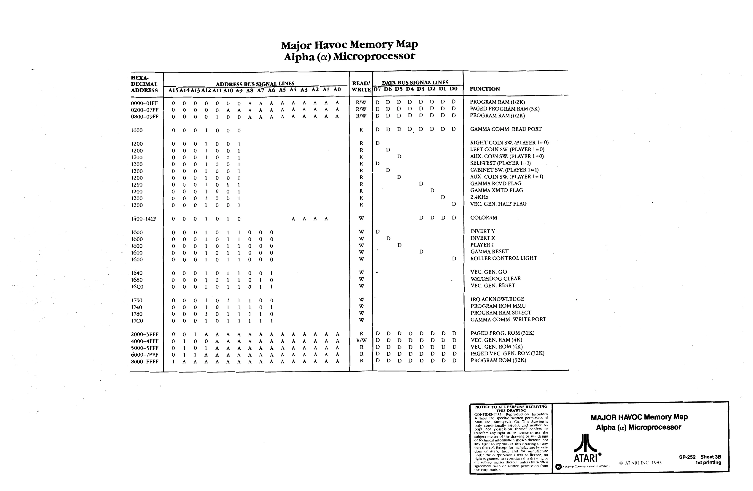
Major Havoc Memory Map Alpha (a) Microprocessor
HEXA-
DECIMAL ADDRESS BUS SIGNAL LINES
ADDRESS FUNCTION
| 0000~01FF | 0 | PROGRAM RAM (1/2K) | |||
| 0200-07FF | 0 | A | PAGED PROGRAM RAM (3K) | ||
| 0800-09FF | 0 | i} | PROGRAM RAM (1/2K) | ||
| 1000 | 0 | 0 | R | GAMMA COMM. READ PORT | |
| 1200 | 0 | 0 | 0 | R | RIGHT COIN SW. (PLAYER 1=0) |
| 1200 | 0 | 0 | 0 | R | LEFT COIN SW. (PLAYER 1=0) |
| 1200 | 0 | 0 | 0 | R | AUX. COIN SW. (PLAYER 1=0) |
| 1200 | 0 | 0 | 0 | R | SELFTEST (PLAYER 1=1) |
| 1200 | 0 | 0 | 0 | R | CABINET SW. (PLAYER 1=1) |
| 1200 | 0 | 0 | i} | R | AUX. COIN SW. (PLAYER 1=1) |
| 1200 | 0 | 9 | 0 | R | GAMMA RCVD FLAG |
| 1200 | a0 | 0 | 0 | R | GAMMA XMTD FLAG |
| 1200 | o | 0 | 0 | R | 2.4KHz |
| 1200 | 0 | oO | 0 | R | VEC. GEN. HALT FLAG |
| 1400-141F | 0 | 0 | 1 | Ww | COLORAM |
| 1600 | 0 | 0 | Ww | INVERT Y | |
| 1600 | 0 | 0 | Ww | INVERT X | |
| 1600 | 0 | 0 | Ww | PLAYER I | |
| 1600 | 0 | 0 | Ww | GAMMA RESET |
1600 0 Oo Ww ROLLER CONTROL LIGHT
| 1640 | 0 | Ww | VEC. GEN. GO |
1680 0 Ww WATCHDOG CLEAR
16CO 0 Ww VEC. GEN. RESET
| 1700 | to} | w | IRQ ACKNOWLEDGE | * |
| 1740 | 0 | Ww | PROGRAM ROM MMU | |
| 1780 | 0 | Ww | PROGRAM RAM SELECT | |
| 17CO0 | 0 | Ww | GAMMA COMM. WRITE PORT | |
| 2000-3FFF | 0 | R | PAGED PROG. ROM (32K) | |
| 4000-4FFF | 1 | RW | VEC. GEN. RAM (4K) | |
| 5000-SFFF | 1 | R | VEC. GEN. ROM (4K) | |
| 6000-7FFF | 1 | R | PAGED VEC. GEN. ROM (32K) | |
| 8000-FFFF | A | R | PROGRAM ROM (32K) |
NOTICE TO ALL PERSONS RECEIVING ‘THIS DRAWING Hn ey” CA ae MAJOR HAVOC Memory Map only eeaonaly, ues ang seine. Alpha (a) Microprocessor transfers any tight in, or license to use, the subject matter of the drawing or any design of (echnical information shown thereon, nor any right (o reproduce this drawing or any part thereor. Except for manufacture by ven: dors of Atari, Inc, and for manufacture wate aca sg ATARI” SP-252 Sheet 38 the subject matter tHereot unless by written the corporation © ATARI INC. 1983 1st printing
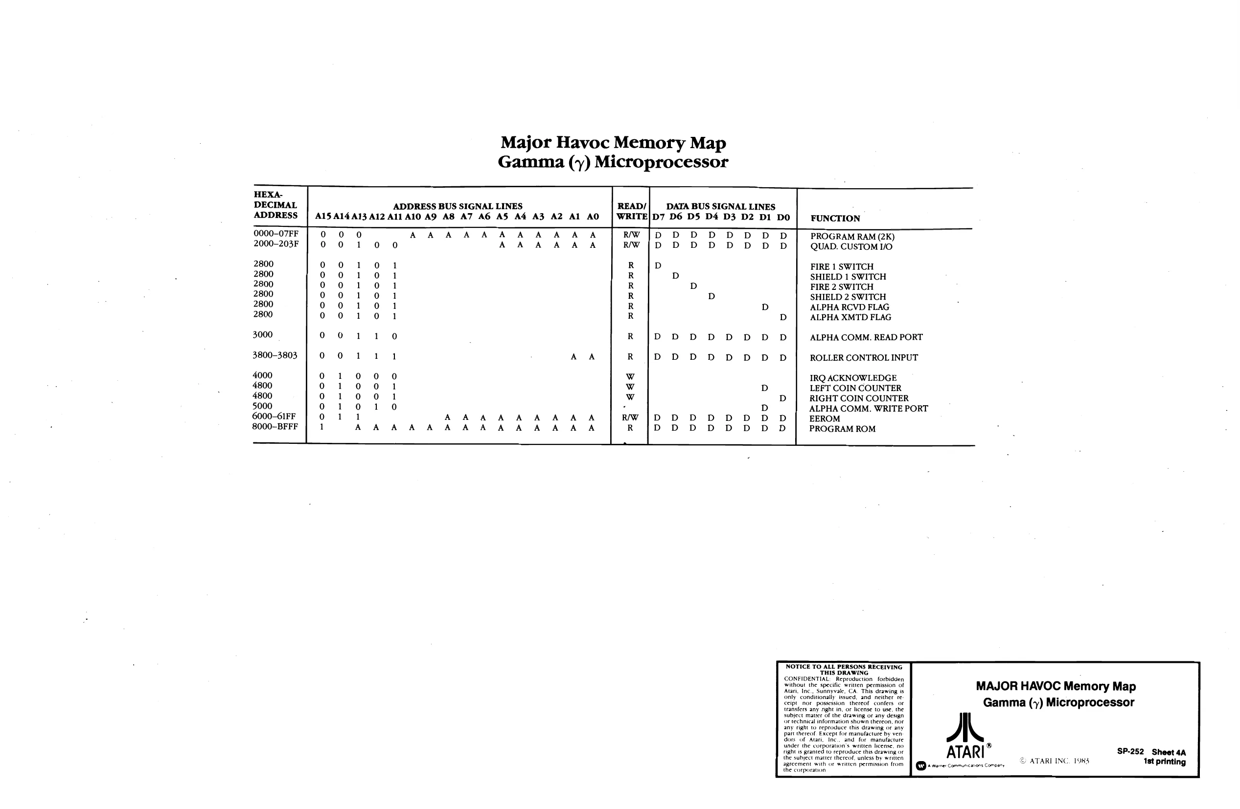
Major Havoc Memory Map Gamma (7) Microprocessor
ADDRESS BUS SIGNAL LINES A15 A14A13 Al2 All A10 A9 A8 A7 A6 AS A4 AZ A2 Al AO FUNCTION 0000-07FF 2000-203F A A A A A A A A A AA 0 0 10 0 A A A A A A PROGRAM RAM (2K) QUAD. CUSTOM I/O
2800 FIRE 1 SWITCH
2800 SHIELD 1 SWITCH
2800 FIRE 2 SWITCH 2800 SHIELD 2 SWITCH 2800 ALPHA RCVD FLAG
2800 ALPHA XMTD FLAG
3000 ALPHA COMM. READ PORT
3800-3803 ROLLER CONTROL INPUT
4000 IRQ ACKNOWLEDGE 4800 LEFT COIN COUNTER 4800 RIGHT COIN COUNTER 5000 ALPHA COMM. WRITE PORT 6000-61FF EEROM 8000-BFFF PROGRAM ROM
NOTICE TO ALL PERSONS RECEIVING THIS DRAWING CONFIDENTIAL: Reproduction forbidden, ‘without the specific written permission of Atari, Inc., Sunnyvale, CA. This drawing is only conditionally: issued, and neither te Ccipt_nor possession thereof confers or transfers any right in, or license to use, the MAJOR HAVOC Memory Map
subject matter Of the drawing or any design Or technical information shown thereon, nor any right to reproduce this drawing or any part thereof Except for manufacture by ven. dors of Atari, Inc., and for manufacture uader the corporation's written license, no ®
© ATARI INC. 1983 SP-252 Sheet 4A Ist printing
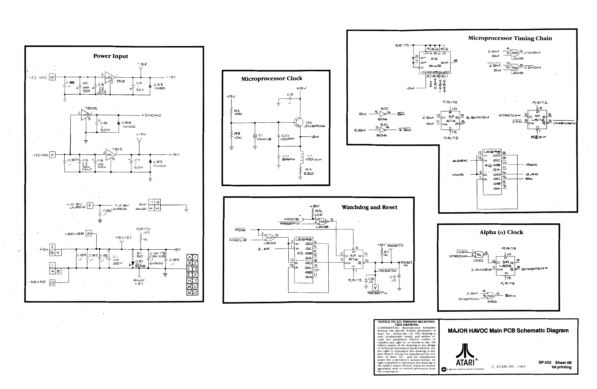
This page is a drawing, shown as the original scan.
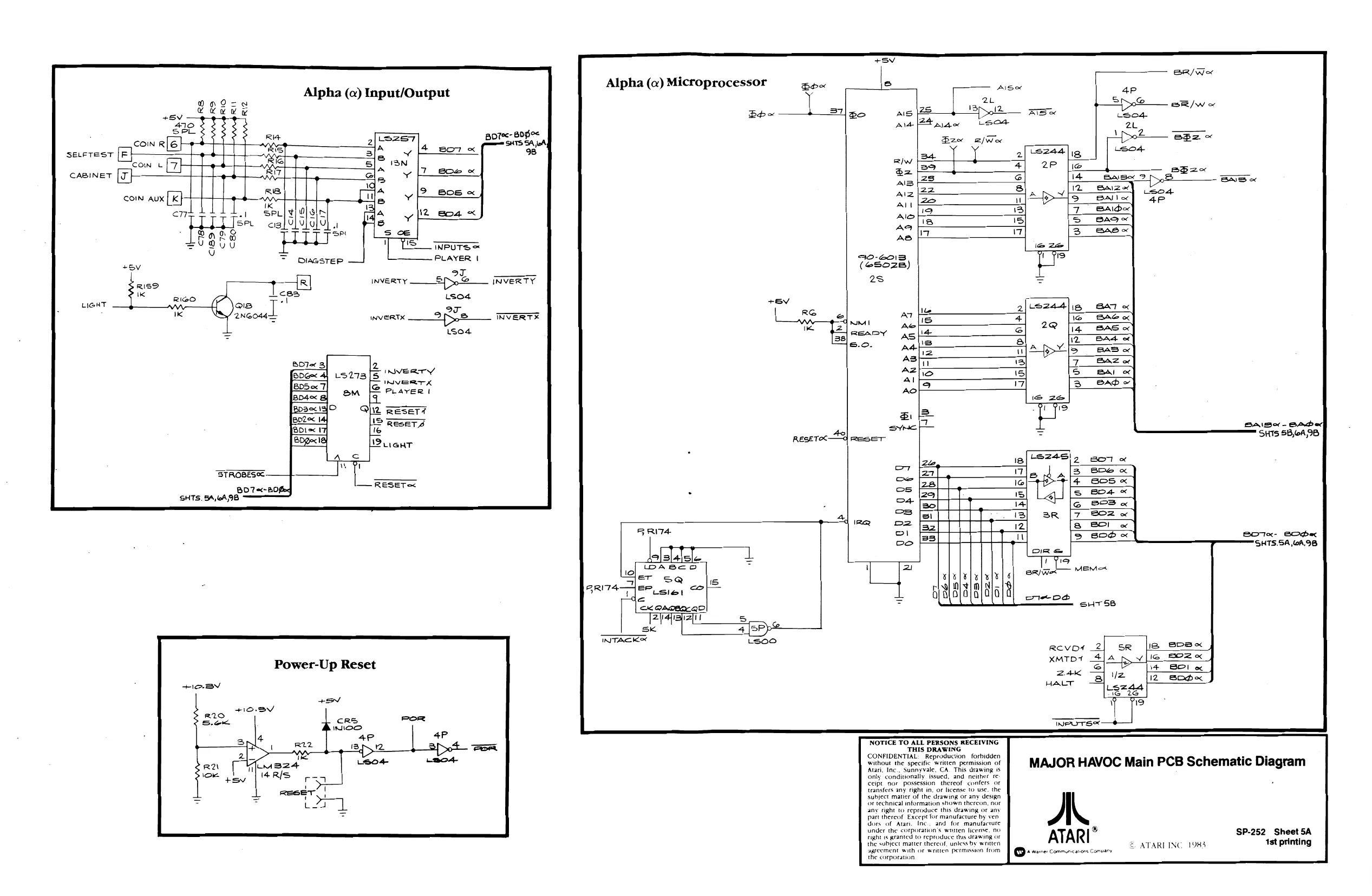
This page is a drawing, shown as the original scan.
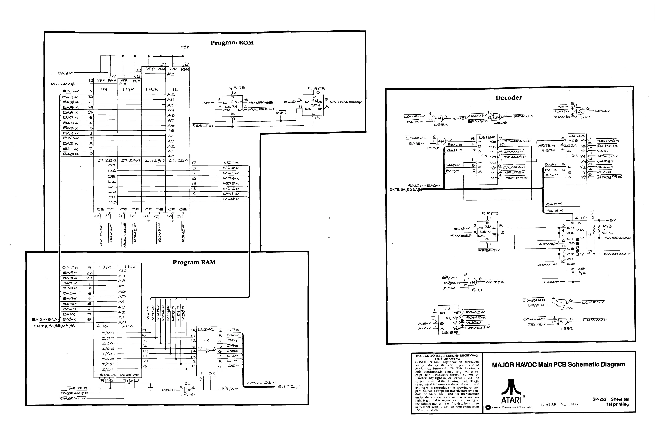
This page is a drawing, shown as the original scan.
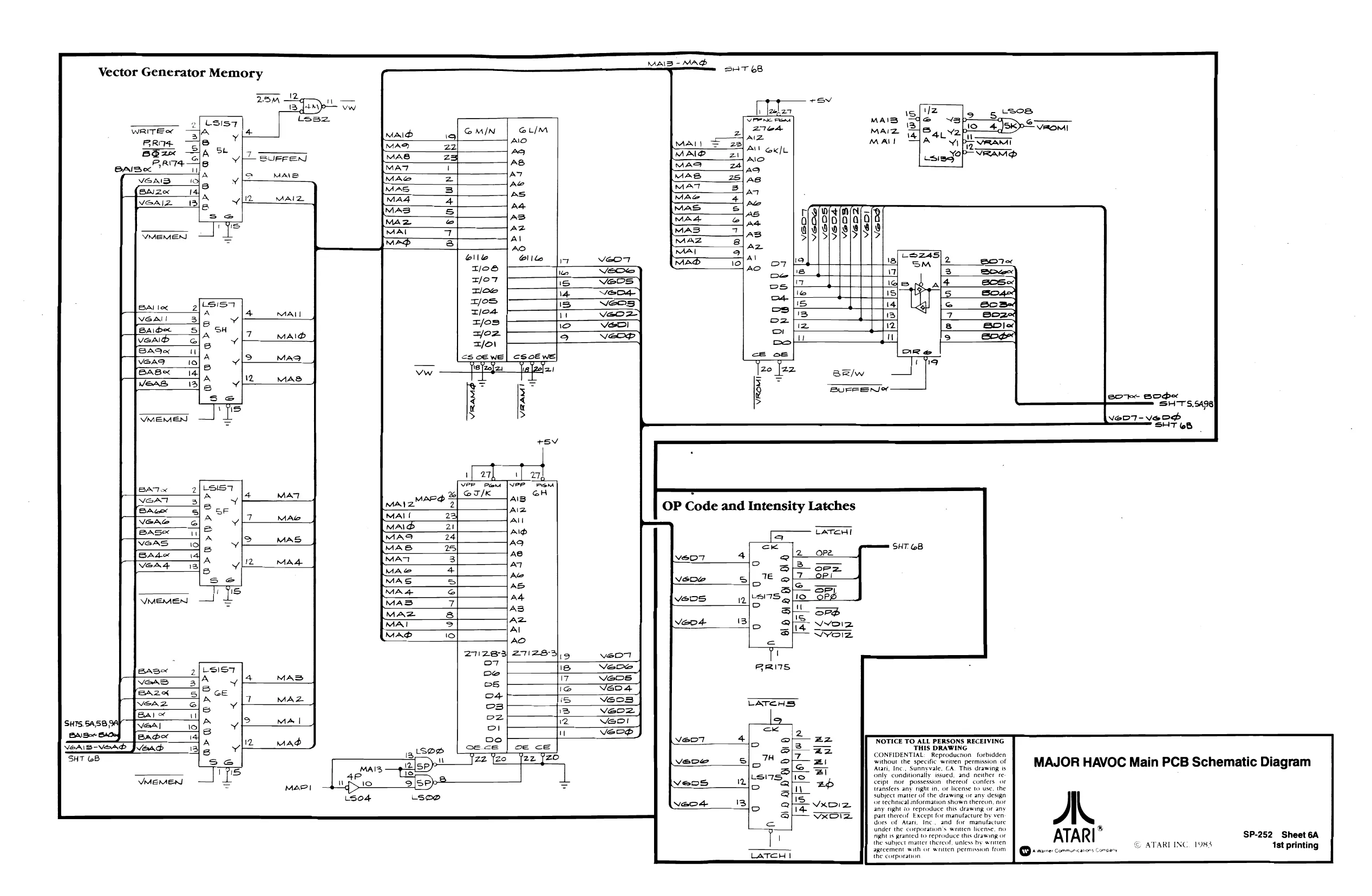
This page is a drawing, shown as the original scan.
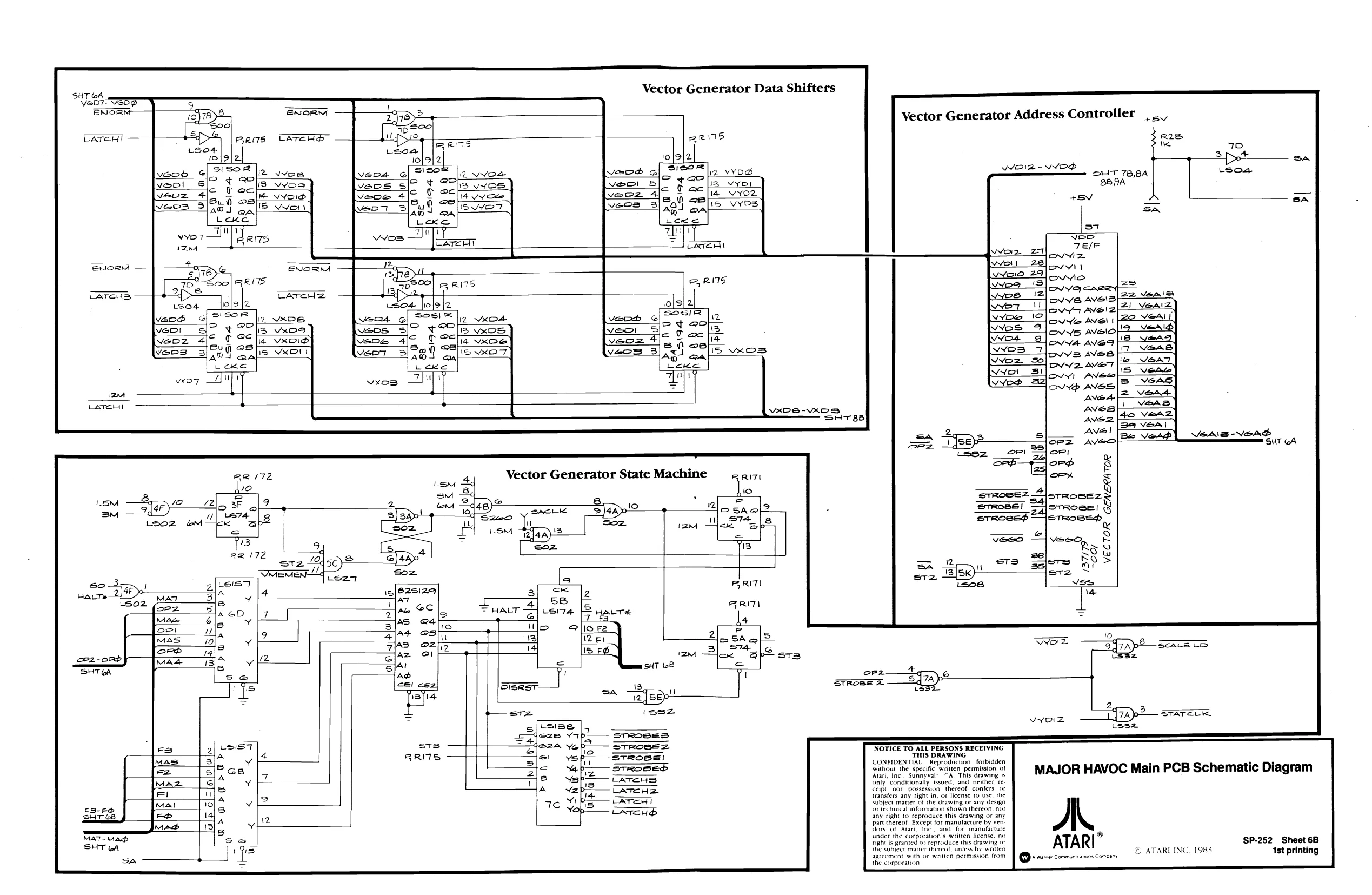
This page is a drawing, shown as the original scan.
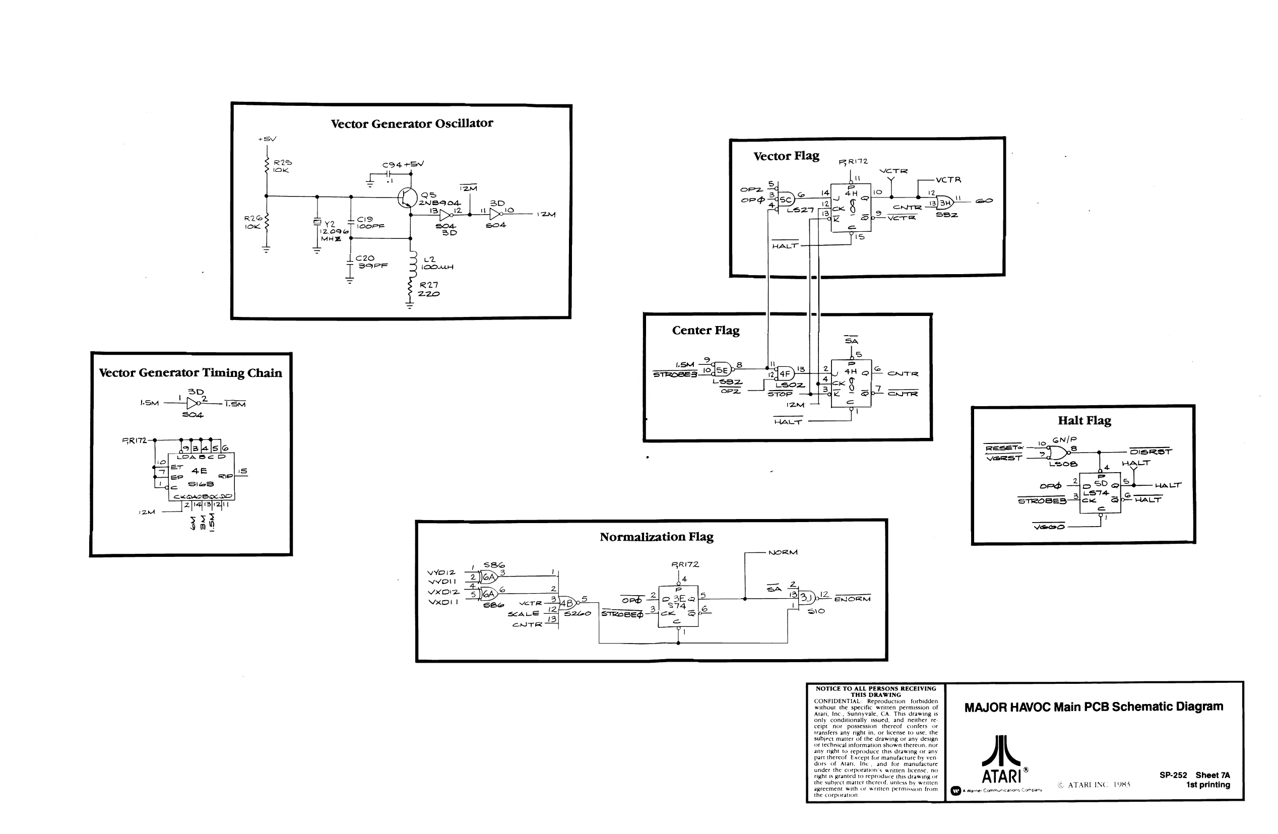
This page is a drawing, shown as the original scan.
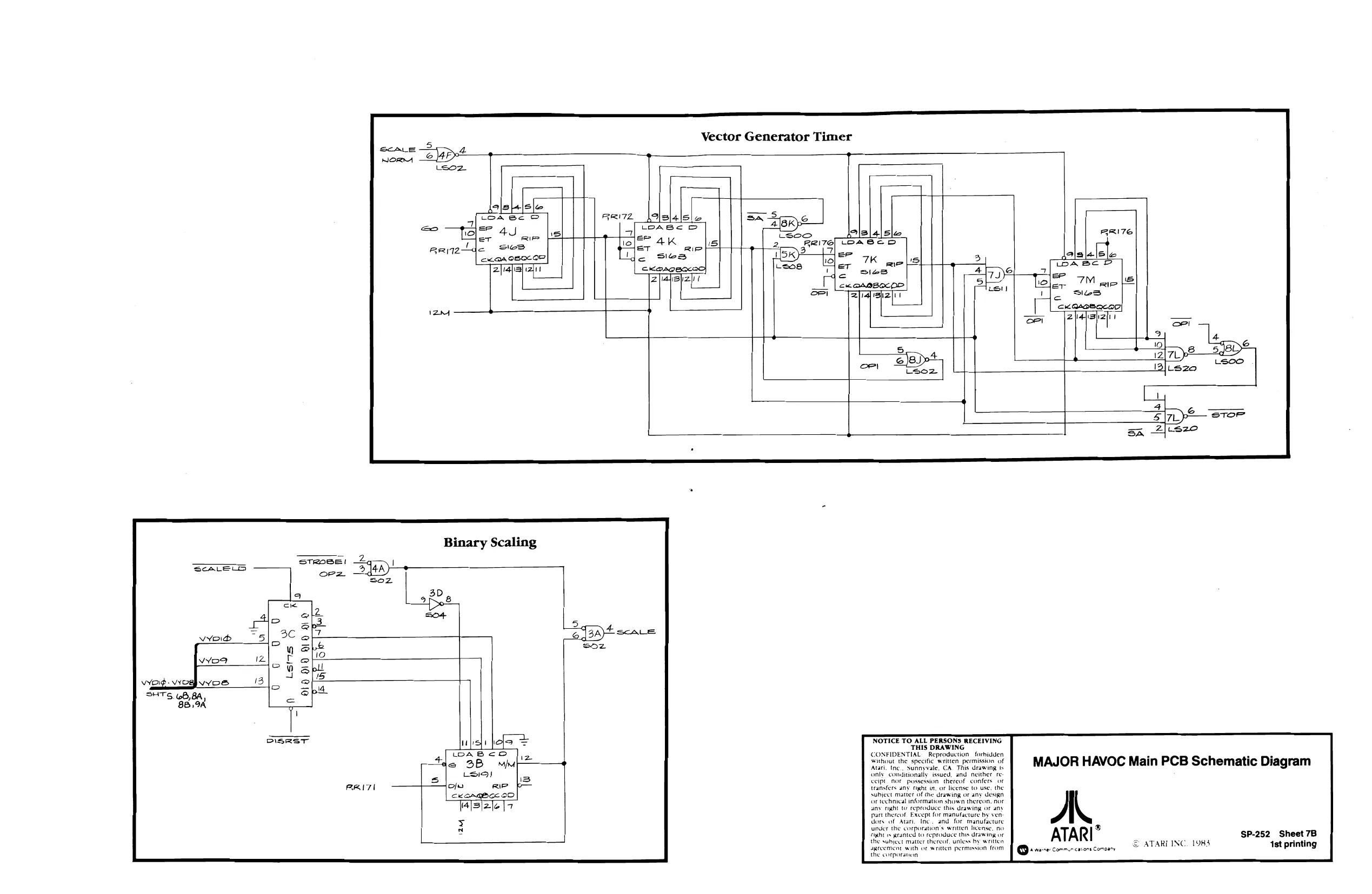
This page is a drawing, shown as the original scan.
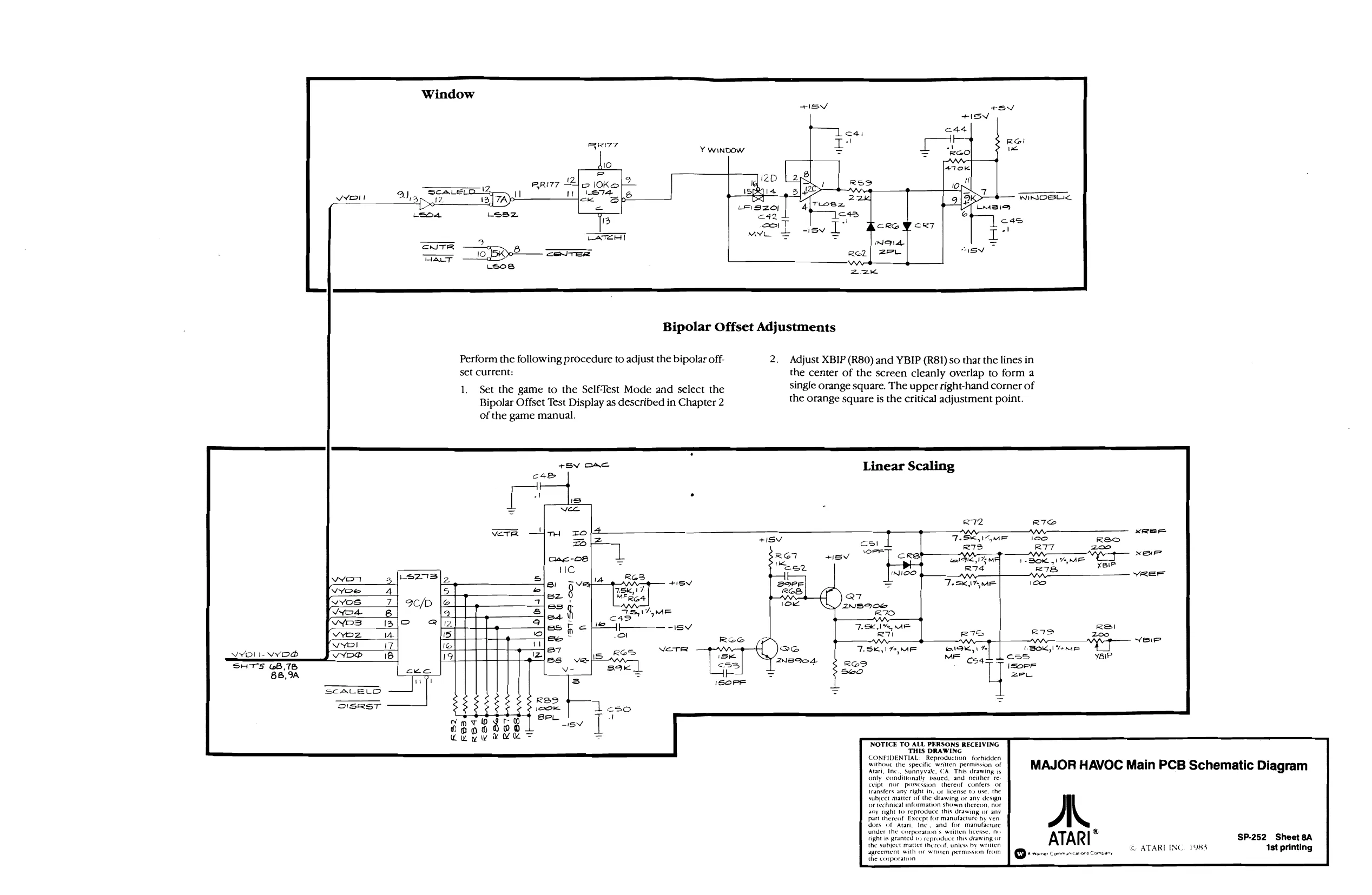
Y winpow
CNTR TACT
Bipolar Offset Adjustments
Perform the following procedure to adjust the bipolar off- 2. Adjust XBIP (R80) and YBIP (R81) so that the lines in set current: the center of the screen cleanly overlap to form a
- Set the game to the Self-Test Made and select the single orange square. The upper righthand corner of Bipolar Offset Test Display as described in Chapter 2 the orange square is the critical adjustment point. of the game manual.
Linear Scaling
R72
| Tae | SS | REO |
| RIS | RTT | Zoo |
1a 51% a Yo rAe= — ae arr a eae 5 37 vont R
| 74 | R78 | yRe= |
Te 10
Je 1% AE Re
| 71 | RID | RTD | 200 | wine |
VYD!II-VYDad MF cog it css Yair Reo IsoPF Seo Zeu
NOTICE TO ALL PERSONS RECEIVING THIS DRAWING CONFIDENTIAL. Reproduction forbidden . . sithoun the speci ren perm ut MAJOR HAVOC Main PCB Schematic Diagram
subject matter of the drawing or any design fr technical information shown thereon, a0 any right to reproduce this drawing or any part thereat Except for manufacture by ven dors of Atari, Inc, and for manufacrare ted wo eproduce this deawing or bd SP-252 She Pear epee ATARI < atant isc 1988 caer otic agreement inn writen permsin 0M | Qs none conmacirs Conary
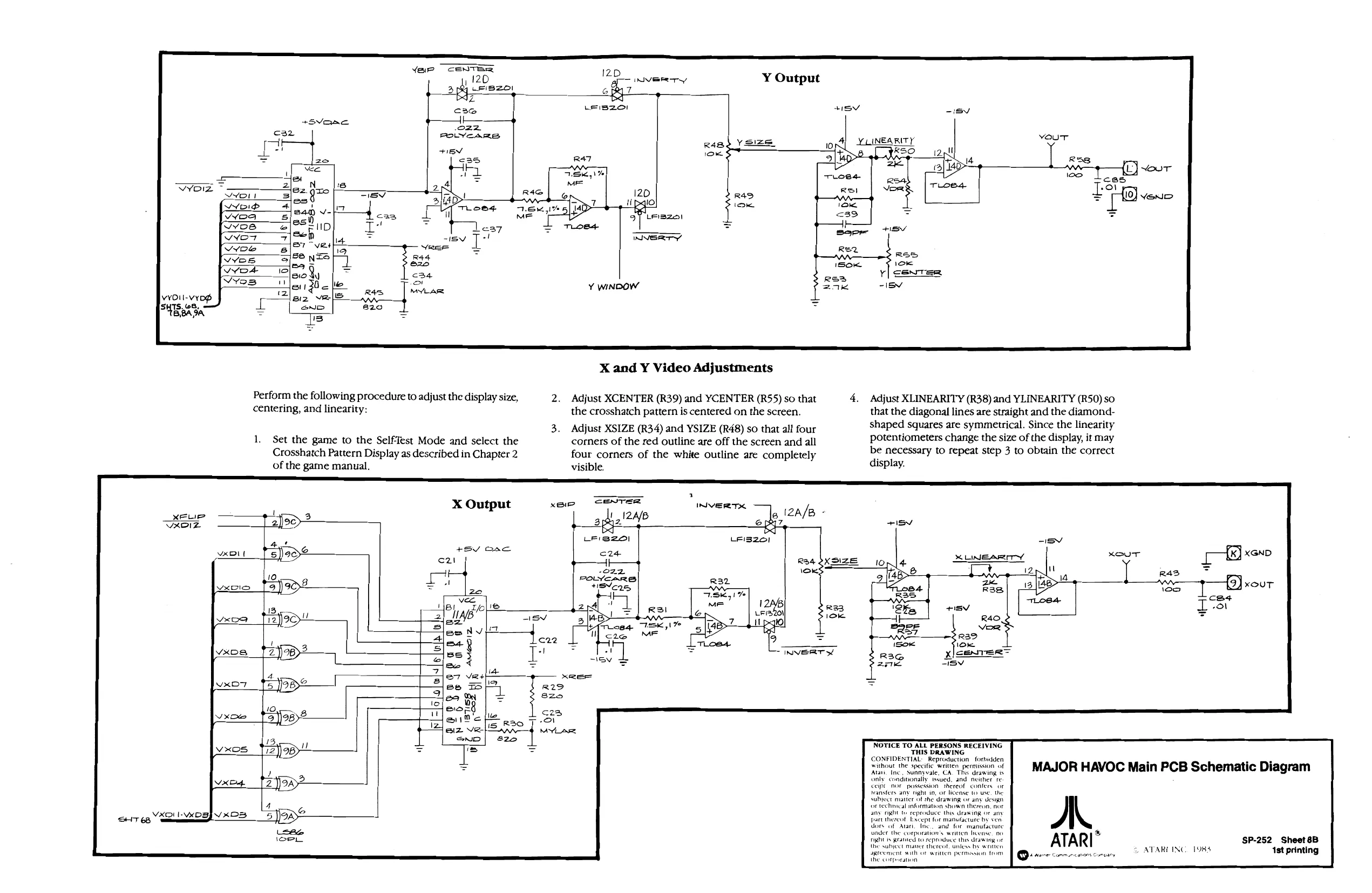
Perform the following procedure to adjust the display size, centering, and linearity:
- Set the game to the Self‘est Mode and select the Crosshatch Pattern Display as described in Chapter 2 of the game manual.
X Output
ysize R48.
X and Y Video Adjustments
visible. Adjust XCENTER (R39) and YCENTER (R55) so that the crosshatch pattern is centered on the screen.
Adjust XSIZE (R34) and YSIZE (R48) so that all four corners of the red outline are off the screen and all four corners of the white outline are completely Adjust XLINEARITY (R38) and YLINEARITY (R50) so that the diagonal lines are straight and the diamondshaped squares are symmetrical. Since the linearity potentiometers change the size of the display, it may be necessary to repeat step 3 to obtain the correct display.
a INVERTX
a= Losg TSK ,17 iI c2e MF
VXO1I-VxDBJV KOS HT 68 xouUT R24 SXSIZE R43 4 id
- xour
NOTICE TO ALL PERSONS RECEIVING THIS DRAWING CONFIDENTIAL: Reproduction formdden without the specific written peemission af Atani Inc, Sunnyvale, CA. Tha drawing 1s only conditionally issued, and neither te Ceipl MOF possession thereof conters oF Faansters any night in, oF license {) USC. Die subject matter of the drawing or any design, or technical information shown thereon, aor any right ti reproduce this drawing or any part thercol_ Except for manufacture by ven dors of Atari Ine. and for manufactute under the corporation's weiten Iikense, 10 rights granted te reproduce this drawing oe the subject mauer thereot, Unies by weitten, agreement wath oF weiter peemasion tron the conparation, A ATARI® sree: commincanons company » ATARE INC Toi
MAJOR HAVOC Main PCB Schematic Diagram
19oRs ca4
SP-252 Sheet 6B 1st printing
This page is a drawing, shown as the original scan.
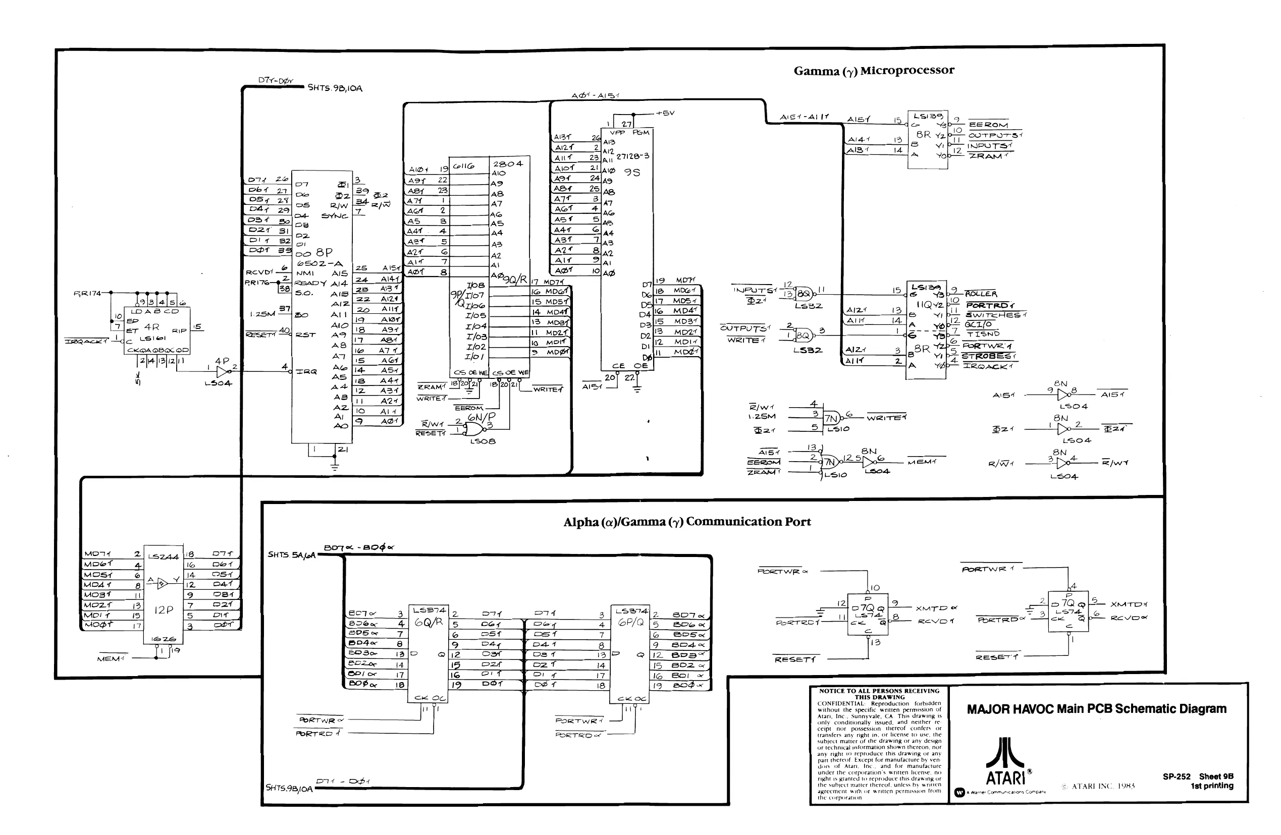
Gamma (y) Microprocessor DTr-ogy SHTS.9B,10A
+Sv AS t-Al IT
vePp POM
AD Ad Au Ae 9S 24/49 Ae
AG
Shas
Aat Clay =
a BEROM SOTPOTSt
INPOTS* ZRAM“ 21128°3
1A AD At tolag
Alpha (a)/Gamma (7) Communication Port
RESETT
NOTICE TO ALL PERSONS RECEIVING THIS DRAWING CONFIDENTIAL: Reproduction. forbitden without the specific written permission of Atari, Inc, Sunnyvale, CA. This drawing is, only conditionally issued, and neither re: Ceipt AOE possession thercof confers or transfers any right in, oF license to use, the Subject matter of the drawing or any design Or technical snformation shown thereon, nor any right 10 reproduce this drawing or any part thereof Except for manufacture by ven: Uo of Atac, Ine... and for manufacture Under the corporation's wri no.
fight 1 granted to reproduce this drawing of
the subject matter thereof, unless by written agreement sith oF seritten permission [rom the corporation PORTRD AL
© ATARI INC. 1984 1 Communications Comoany
MAJOR HAVOC Main PCB Schematic Diagram
ATARI ® ; SP-252 Sheet 9B 1st printing
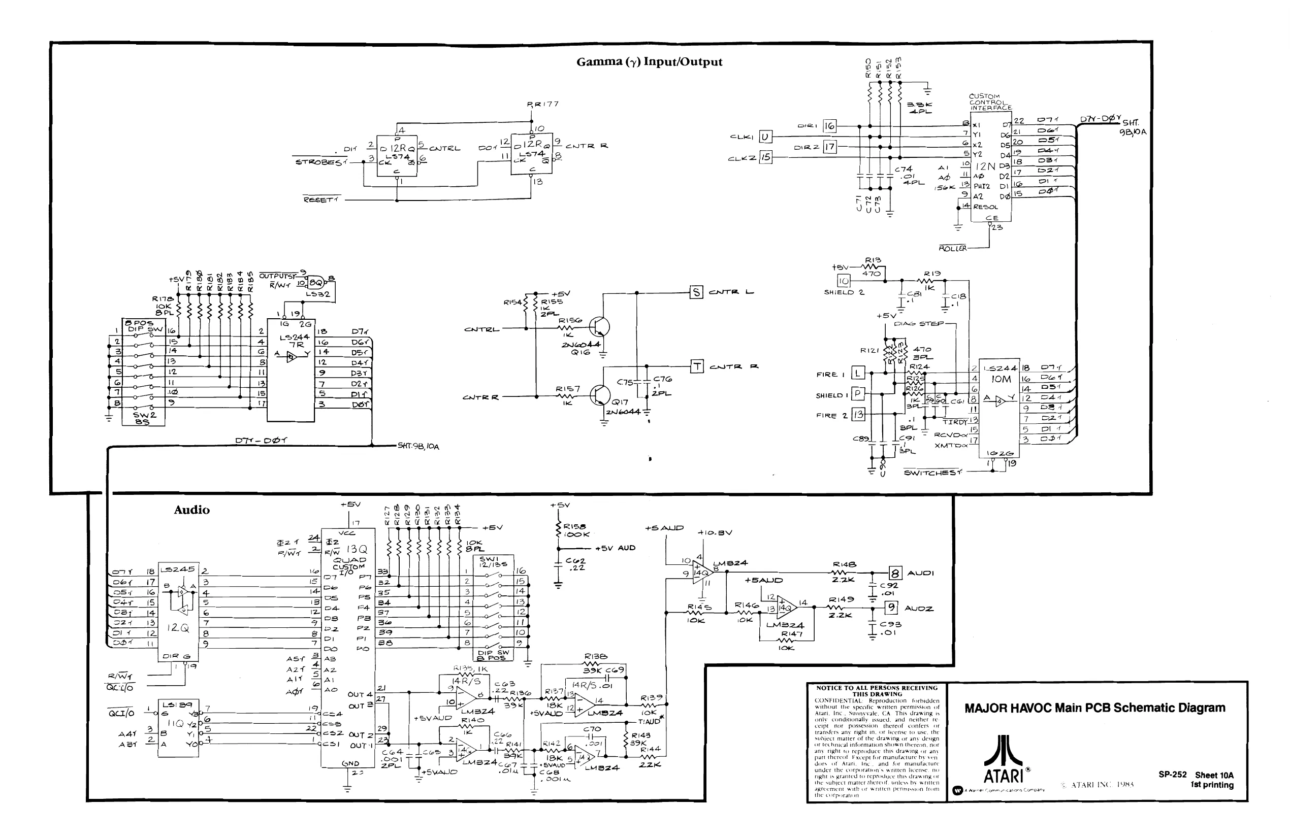
This page is a drawing, shown as the original scan.