Slither
Slither (set 1) (Century II (GDI license), 1982) · Manual · 49 pages · 26 sections · original scan
SLITHER
OWNER-OPERATOR SERVICE MANUAL
5945 North Rogers Ave. Chicago, Illinois 60646 (312) 286-6722
16A-20968
CONTENTS
Component location Game set-up and adjustments Color monitor setup instructions Self test mode Theory of operation Troubleshooting Additional troubleshooting information Power requirements Video board component layout Video board parts list DSR board component layout DSR board parts list Schematics Cabinet Wiring Video CPU Board Data/Sound/ROM Board (DSR Board) Power Supply Monitor (Wells-Gardner 19K 4951) Page
Oona
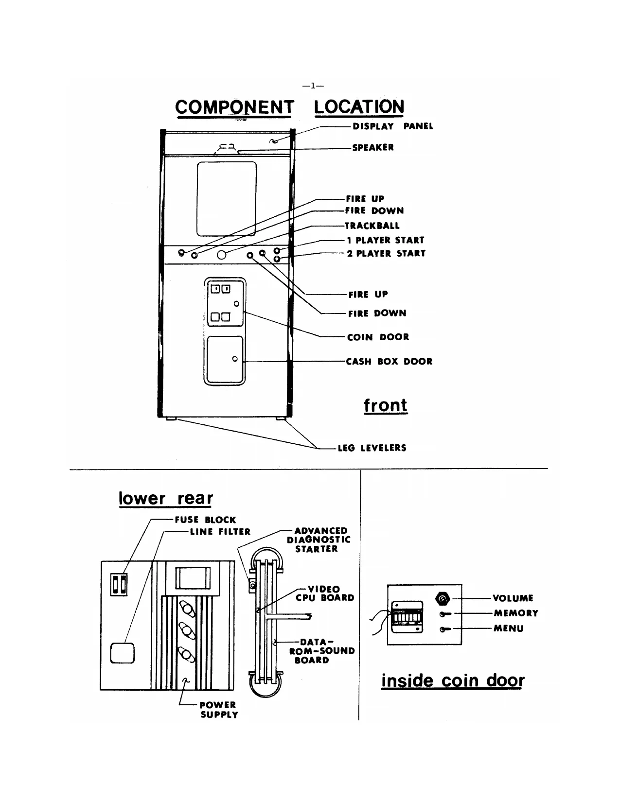
This page is a drawing, shown as the original scan.
GAME SET-UP_& ADJUSTMENTS
MEMORY PROTECT SWITCH
The Memory Protect Switch is used to prevent erroneous writes to locations in the CMOS RAM which store the location program variables selected from the LOCATION PROGRAMMING MENU, After any changes are made to this menu on the screen, it is necessary to hold the MEMORY PROTECT BUTTON while at the same time depressing the 2 PLAYER SELECT BUTTON in order to save screen changes
and load them into CMOS RAM. (See Location Programming below. )
MENU BUTTON
To gain access to the various location and self test programming menus, the game is supplied with a Menu Button located inside the coin door. Activation of this button while the game is in the attract mode will place the operator in the AUDIT DISPLAY. From there, the player controls are used to advance to the next menu and to make any changes. Instructions on the screen show how this is done.
VOLUME CONTROL SETTING
A Volume Control for the game is located inside the coin door for quick volume adjustment within a limited range, The master volume control is located on the DSR logic board,
COIN METER
A 12 volt DC coin meter is located inside the coin door and is used to keep a count of all coins in the cash box. This meter is pulsed once for each coin in regardless of the coin chute used.
AUDIT DISPLAY
Push the menu button located inside the coin door one time with the game in the attract mode to display the audit menu. The audit display should look like this:
AUDIT DISPLAY
| TOTAL GAMES PLAYED | XXX | (cannot be reset, default 0) |
| GAMES PLAYED | 0 | (resetable to 0, default 0) |
| MINUTES PLAYED | 0 | (resetable to 0, default 0) |
| BONUSES AWARDED | 0 | (resetable to 0, default 0) |
| CENTER COIN SLOT | 0 | (resetable to 0, default 0) |
| RIGHT COIN SLOT | 0 | (resetable t0 0, default 0) |
| LEFT COIN SLOT | 0 | (resetable t0 0, default 0) |
USE FIRE UP FOR NEXT MENU (To Location Programming) USE PLAYER 1 TO CLEAR AUDITS (reset above to zero) USE PLAYER 2 TO CLEAR SCORES (reset HIGH SCORES) USER FIRE DOWN TO EXIT (return to attract mode)
The default values given are entered when the CMOS RAM has failed to retain data. This may happen if the logic boards are removed from the machine, or the NI-CAD battery has been discharged. Charging of the NI-CAD battery is automatic if the game is left on, but the battery may become discharged if the game is left off for more than about 6 days. If this is the case the game will come up with the message "CMOS Invalid Requires Service" when first turned on. If the game comes up in the normal attract mode, CMOS RAM data is okay. See location programming below.. IT IS NOT NECESSARY TO HOLD THE MEMORY PROTECT SWITCH WHEN RESETTING THE HIGH SCORES OR THE AUDIT TOTALS. Actuate the memory protect switch to go from the service message to the location programming menu.
LOCATION PROGRAMMING MENU
From the AUDIT DISPLAY hit the FIRE UP BUTTON to access the LOCATION PROGRAMMING MENU. If the game displays the CMOS invalid message after it is first turned on, the data held in the CMOS RAM has been lost. (See above.) If this is the case, the game must be reprogrammed either with operator selected values or with the default values, If the game comes up in the norma’ attract mode when first turned on the previously saved values are valid. The player controls are used to change the values on the screen and to recall the factory default settings if desired, IMPORTANT ---- CHANGES MADE TO THE SCREEN VALUES ARE NOT LOADED INTO CMOS MEMORY UNLESS THE MEMORY PROTECT SWITCH IS HELD WHILE AT THE SAME TIME THE PLAYER 2 BUTTON IS PRESSED. HOLD THE MEMORY PROTECT SWITCH LONG ENOUGH FOR THE GAME TO RETURN TO ATTRACT MODE. Failure to exit the location programming menu in this manner will cause no changes in values even though changes have been made to the values on the screen.
The location programming menu should look Ti his:
LOCATION PROGRAMMING MENU
USE FIRE DOWN TO ADVANCE ITEM (move cursor) _ USE FIRE UP TO EXIT (return to attract with NO changes) USE TRACKBALL TO SELECT VALUE (move ball up or down) USE PLAYER 1 TO RECALL DEFAULTS (load default values onto screen only) USE PLAYER 2 TO SAVE UPDATES (don't forget the MEMORY PROTECT SWITCH! )
BONUS LEVEL 000Xx0000 (10 to 25,000 in 5000 increments, default is 15000)
| PLAYS PER GAME | 03 | (shooters to start 1 to 9, default 3) |
| DIFFICULTY | 03 | (1 to 3, default 1) |
| FREE PLAY | N | (N or Y default N (No) |
CENTER COIN MULTIPLIER 04 (0 to 99 coin units per coin, default 4)
| RIGHT COIN MULTIPLIER | 01 | (0 to 99 coin units per coin, default 1) |
| LEFT COIN MULTIPLIER | 01 | (0 to 99 coin units per coin, default 1) |
| COIN UNITS CREDITS | 01 | (0 to 99 coin units for credit, default 1) |
| COIN UNITS BONUS | 00 | (0 to 99 bonus credit level, default 0) |
| CREDITS COIN LOCK | 10 | (0 |
to 99 credits to de-engerize coin
lockout coils (optional), default 10)
| COCKTAIL OPTION | N | (N for upright or Y for cocktail, default N) |
In order to leave the LOCATION PROGRAMMING MENU without making any changes hit the FIRE UP BUTTON. This will return the game to the attract mode, In order to leave theLOCATION PROGRAMMING MENU and load the factory default values first hit the PLAYER 1 BUTTON to load the defaults to the screen and then hold the MEMORY PROTECT SWITCH and press the PLAYER 2 BUTTON, Be sure to hold the memory protect switch long enough for the game to return to the attract mode,
t+++ THE DEFAULT PRICING IS 1 PLAY PER COIN +4+++
BONUS LEVEL - This is the score level at which extra shooters are awarded. The default level is 18,000 points. This level may be adjusted from 10 to 25 thousand in 5 thousand point increments, Extra shooters are awarded at all even multiplies of this value. For example, if this value is set to 15,000 then bonus shooters are awarded at 15,000, 30,000, 45,000, 60,000 etc., etc. points.
PLAYS PER GAME - This is the number of shooters given at the start of the game. The default value is 3 shooters. This value may be adjusted from 1 to 9
DIFFICULTY - The difficulty setting changes the game in a subtle manner to make the game easier or more difficult to play. The default setting is 1. This adjustment can be in the range of 1 to 3, with 1 the easiest and 3 the hardest.
FREE PLAY - The free play mode is primarily intented for use in showrooms and at conventions or for home use. The default is N for no or normal pricing. Set to Y for yes and free play if desired. Setting the game to free play does not affect the attract mode.
CENTER COIN MULTIPLIER, RIGHT COIN MULTIPLIER AND LEFT COIN MULTIPLIER - Each of the coin multipliers are set up to multiply the number of coins dropped into the appropriate coin slot by a fixed value to award COIN UNITS. One coin in would equal some number of coin units. Credits needed to play the game are awarded when some number of coin units has been reached as defined in the following two adjustments. The default values are center 4, left 1, right 1, The center coin chute is not available on the coin door supplied and is not wired. Any of the three multipliers may be set anywhere from 0 to 99 coin units per coin in.
COIN UNITS PER PLAY - This value is the number of coin units necessary to award one credit. The coin unit total is no displayed at any time and is reset to zero at the start of play. The credit total is displayed and is decremented by one for each player at the start of a game. The default value is 1 and this may be set from 0 to 99.
COIN UNITS PER BONUS - This is the level of coin units at which a bonus or extra credit is awarded, It is used when incentive pricing is desired such as 1 play for 25¢ and 3 plays for 2x 25¢. Reaching the bonus level
resets the coin unit total to zero so that working toward the next bonus starts over. The default level is 0 (no bonus) and this may be adjusted to any value from 0 to 99. If this all is a bit confusing, the following tables for various pricing schemes will be of value. The tables show settings for three coin chutes, even though the center chute is not provided on the coin door.
a ud ao i
| Go | #4 | 6 | 8 | |
| a | 2 | 4 | @ | 2 |
| a | _ | a | a Oo | |
| =s | 5 | —- | °° | 8 |
| at > | a | a | a | |
| > | = | 2 | & | ®@& |
= —4
| — | = | nn ” | ||
| = oO | — | a | raed | ||
| = | 8 | 5s | £ | E |
| 3 | 8 | 2B | 2 | |
| oO | a | > | > |
uu i
| | val Ee a | = | =z | ||
| mc | & | 6 | £ | & |
| PRICING DESIRED | 4s | 6&6 | &@€ | 8 §& |
| DEFAULT USA | 1/25¢, 4/$1 | 01 04 01 ol 00 |
USA 1/50¢, 3/$1, 6/$2 01 04 O1 02 04 1/50¢ 01 04 O01 02 00 FORIEGN
| 1DM, 5DM door | 1/1DM, 6/5DM | 06 00 Ol ol 00 |
| 1 FRANC, 5 FRANC door | 1/2F, 3/5F only | 01 16 #06 02 00 |
25 cents, 1 Guilder door 1/25, 4/16 01 00 04 01 00
| 5 FRANCS, 10 FRANCS | 1/5F, 2/10F | 01 00 02 o1 00 |
| 5 FRANCS, 10 FRANCS | 1/10F | 01 00 02 02 00 |
| 1 UNIT, 5 UNITS | 1/2, 3/5 | 01 00 06 02 00 |
| TWIN COIN | 1/1 coin | 01 00 ol Ol 00 |
| TWIN COIN | 1/2 coins | 01 00 01 02 00 |
CREDITS COIN LOCK- Sets the level of credits at which time the optional coin lockout coils are de-energized and further insertion of coins is prohibited, The setting of CREDITS COIN LOCK does not affect the operation of the coin switches or other pricing. The default value is 10 and may be set in the range of 0 to 99, Coin lockout coils are not standard equipment on the coin door and the wiring in the cable harness is not provided. Coin lockout coils and the necessary wiring may be added in the field if necessary.
COCKTAIL OPTION- The default value is N for the upright game, and may be changed to Y for the cocktail version, The cocktail version flips the picture for player 2 and expects a second set of player controls.
COLOR MONITOR SETUP_INSTRUCTIONS 69X1179-100
cen onive onive RED CUTOFF. GRN CUTOFF
| eu cutorr | xago1 | Khosz |
NEG H Sync
| NEG V SYNC | WHEN bsma.coue | k4902 | K4956 |
Cj
| ono | posite sync USE | yom | k4906 | KA9S6R |
| Pos H sync, | worizontat sync | wrots | 4911 | K4961 |
POs v SYNC GND Buu GRN RED
‘1 WORIZ VERT VERT VERT VERT _HORIZ. SCREEN CENTERING SIZE HOLD DAMPING RASTER RASTER SHIFT SHIFT
HORIZONTAL FREQUENCY
With the monitor being driven from the game signal, connect a jumper between TP601 and TP31. Adjust the horizontal hold control until picture stops sliding horizontally, remove jumper. Do not use the horizontal hold control for horizontal centering. (See #3) OTE: When game sync is composite, use horizontal sync input.
PICTURE SIZE
Adjust the vertical size control, and the horizontal width coil for desired picture size.
PICTURE CENTERING
1f the video is off center vertically, move the vert raster position adjustment to the up or down position. If the video is off center horizontally, adjust the horizontal video position control to center the picture. If any additional horizontal positioning is required, move horizontal raster position adjustment to the left or right position.
VERTICAL DAMPING
Adjustment of this control is required only if the monitor is being used with a game in which the top several raster lines are visible on the screen. Adjust the vertical damping control for uniform spacing of the top raster lines.
BLACK LEVEL
Adjust the black level control to obtain the proper black level (the black Portion of the picture just extinguished). Do not use the screen control to set the black level.
FOCUS Adjust the focus control for best overall definition and fine picture detail.
SELF TEST MODE
To enter the Self Test Mode, press the Self Test Button located on the Video PCB near the LED display. All the LED's should blink on and the Hardware Tests should start. If at anytime during the hardware tests the machine halts for more than ten seconds, there has been a detected failure. A brief description of a few tests and probable chip failures are contained in the following section (Hardware Tests), but for more extensive repair, refer to the Troubleshooting Guide found elsewhere in this manual.
HARDWARE TESTS
- Video Board ROM Checksum The ROM Checksum calculates the checksum of each Video ROM and compares it to the checksum stored for that ROM. If it differs from the stored value, the machine will halt and the value of the LED s can be referenced to the faulty ROM by the following table.
VIDEO BOARD ROM CHECKSUM LED VIDEO
| VALUE | ARDRESS | 2716 | 2732 |
| 01 0000 | A000-A7FF | N/A | U4l |
| 01 0001 | A800-AFFF | N/A | U41 |
| 01 0010 | BOOO B7FF | N/A | U40 |
| 01 0011 | B800- BFFF | N/A | U40 |
| 01 0100 | C000-C7FF | U43 | U39 |
| 01 0101 | C800 -CFFF | U42 | 039 |
| 01 0110 | DO00-D7FF | val | U38 |
| 01 0111 | D800-DFFF | U40 | U38 |
| 01 1000 | E000-E7FF | u39 | U37 |
| 01 1001 | E800 -EFFF | U38 | U37 |
| 01 1010 | F000-F7FF | U37 | U36 |
| O1 1011 | F800-FFFF | U36 | U36 |
The EPROM Memory in a given game may be implemented as banks of either 2716 or 2732 EPROMS. The EPROM type for the video bank is selected by the decoding jumper (JUMP PLUG 1).
2, Communications RAM from Video Board The Communications RAM test determines the stability of memory shared by the two processors by storing a predefined series of numbers throughout the RAM, then reading it back to insure that it was stored correctly.
Failure Code 00 0010
3, __ Video Board CMOS RAM After saving values in another portion of memory, the CMOS RAM is tested in the same manner as the Communications RAM. If the CMOS RAM passes the test, all of the locations are restored to their previous values.
Failure Code 00 0011
- Video Board Color RAM This tests the system Color RAM by storing predefined sequences of numbers in the Color RAM, then reading them back while testing for accuracy.
Failure Code 00 0100
- Video Board Screen RAM The Screen RAM is tested by writing a pattern to each page on the screen. The results of these writes is then compared to the original pattern. Any discrepancy causes the machine to halt with the LED displaying the faulty RAM. Refer to the following table for decoding the LED patterns.
VIDEO BOARD SCREEN RAM
LED LED
VALUE RAM VALUE RAM
| 10 0000 | U33 | 11 0000 =U66 |
| 10 0001 | U32 | 11 0001 Ué5 |
| 10 0010 | U31 | 11 0010 vU64 |
| 10 0011 | U30 | 11 0011 = =U63 |
| 10 0100 | u29 | 110100 62 |
| 10 0101 | U28 | 11,0101 U61 |
| 10 0110 | U27 | 110110 vé6é0 |
| 10 0111 | U26 | 110111 U59 |
| 10 1000 | ul7 | 11 1000 48 |
| 10 1001 | vl6 | 11 1001 =U47 |
| 10 1010 | uls | 11.1010 U46 |
| 10 1011 | vu14 | 1121011 045 |
| 10 1100 | 13 | 111100 =U44 |
| 10 1101 | U12 | 11:1101 (043 |
| 10 1110 | Ull | 111110 «042 |
| 10 1111 | v10 | 121111 41 |
- DSR Board ROM Checksum The ROM Checksum calculates the checksum of each Data ROM and compares it to the checksum stored for that ROM. If it differs from the stored value, the machine will halt and the value of the LED's can be referenced to the faulty ROM by the following table.
DATA BOARD ROM CHECKSUM LED DATA
| VALUE | ADDRESS | 2716 | 2732 |
| 01 0000 AOQO0-A7FF | N/A | U32 | |
| 01 0001 A800-AFFF | N/A | U32 | |
| 01 0010 8BO00-B7FF | N/A | U31 | |
| 01 0011 8B800-BFFF | N/A | U31 | |
| 01 0100 C000-C7FF | u34 | U30 | |
| 010101 C800-CFFF | U33 | 030 | |
| 010110 DOOO-D7FF | U32 | u29 | |
| 01 0111 D800-DFFF | U31 | U29 | |
| 01 1000 £E0O0-E7FF | U30 | U28 | |
| 01 1001 E800-EFFF | u29 | u28 | |
| Q1 1010 FOOO-F7FF | U28 | u27 | |
| 011011 F800-FFFF | U27 | U27 |
The EPROM Memory in a given game may be implemented as banks of either 2716 or 2732 EPROMS. The EPROM type for the Data bank is selected by the decoding jumper (JUMP PLUG 2).
- DSR Board Local Memory The Data Processor uses a known sequence of numbers to test the bits in Local Memory. If a bad bit is found the machine will halt with the following display.
Failure Code 00 0111
- Communications RAM Addressing The function of this test is to insure that both the Data and the Video Processors address the Communications RAM in the same manner. The Data Processor requests the Video Processor compare the results to the expected pattern. If it does not match, one of thé processors is probably decoding the address incorrectly as the RAM itself was previously tested for stability- by the Video Processor. The machine will halt with the following display if a failure is detected.
Failure Code 00 1000
- Data/Video Handshake This test insures that the Data Processor can send priority commands via interrupts to the Video Processor. The Video Processor is halted, then restarted by the Data Processor after the proper command acknowledgements are received. If a failure occurs, the machine will halt with the following display.
Failure Code 00 1001
During the later portion of the tests the video screen should show some nice pretty colors and finally end up with vertical color bars on the screen. At this time several other tests and displays can be accessed using the FIRE UP BUTTON and the FIRE DOWN BUTTON at the appropiate places. From the color bars press FIRE UP to get to the monitor display subtests.
MONITOR DISPLAY SUBTESTS
GRID- From the color bar display press FIRE UP to get to the first of the monitor subtests, the grid. The grid is drawn in red and then changed to white. From this point press FIRE UP to skip to the I/O TEST or press FIRE DOWN to go to the next monitor subtest. Proceed from one monitor subtest to the next by pressing FIRE DOWN. The monitor display subtests are as follows: WHITE GRID, WHITE DOTS, BLUE DOTS, GREEN DOTS, RED DOTS, ALL WHITE, ALL BLACK.
—1lo—
FULL COLOR DISPLAY
From the monitor display subtests press FIRE UP to display all possible colors on the screen,
1/0 TEST
From the full color display press FIRE UP to proceed to the I/O test. Switch, trackball, and sounds can be tested from this menu. The screen should look something like this:
PIA REG TRACKBALL SOUND TEST PRESS FIRE UP FOR NEXT MENU (proceed to the audit display) PRESS FIRE DOWN NEXT SOUND (advance sounds from 0 (silent) to A) CURRENT SOUND TEST 0 (current sound being exicuted 0 to A)
| 9000 | FF | 4 | F 37 | (PIA at $9000 ~ player switches) |
| 9400 | FF | 4 FF | 4 | (PIA at $9400 - player and coin switches) |
| 9800 | aa | 4 BF 26 | (aa is trackball vert pos. BF sound command) | |
| 9c00 | bb | 4 9F 26 | {bb is trackball horiz pos. 9F for sounds) |
Please note that all of the switches and the trackball should make some change in the above display. Trackball coordinates of 0,0 should put the shooter in the lower left corner of the screen. Make sure that slight movements of the trackball cause the vertical and horizontal position numbers to change one at a time from 00 to FF hex.
Pressing the FIRE UP BUTTON will exit the self tests and place the game in the AUDIT DISPLAY as described in the SET UP & ADJUSTMENTS section of the manual.
—1l—
THEORY OF OPERATION
1.1_ GENERAL
The Century II video game system is a dual multi-processor based system utilizing the Motorola 6809E,
The system consists of two PC Boards. The Video Board and Data/ Sound/Rom (DSR) Board.
A. The Video Board performs all screen display functions, such as play field, line drawing, etc.
B, The DSR Board performs the following functions.
- Contains all necessary ROMs for both video and data processors.
- Generates sounds 3, Contains the data processor which supervises overall operation of the game system.
In order to facilitate inter-processor communication, the data and video micro-processor are running synchronously using clock and timing signals developed on the video board. For this reason, discussion will begin by examining the video board.
2.1 SYSTEM CLOCK
The fundamental system clock is generated by the 21.5 MHz crystal and inverters U24 and U39, This 21.5 MHz signal is divided by high speed flip flop U38 to obtain a 10.75 MHz main clock with a precise 50 percent duty cycle.
This 10,75 MHz signal generates all other fundamental timing signals for the system, including the data processor. IC U23 divides the 10.75 MHz signal down to 5.375 MHz, 2.6875 MHz, 1.34375 MHz, and CCLK. IC's U9, U37, and U38 combine these signals, presenting them to U25, which synchronizes the output signal to the system 10.75 MHz clock.
The performance characteristics of the clock circuits may be noted by referring to timing diagram 1, All signals conform to the limits stated in these diagrams.
2.2 SCREEN RAM
The video processor controls a screen ram of 256 x 256 pixels, with 8 bits per pixel. In order to enable access to this information, the screen is divided into two pages, top and bottom, chosen under software control. These pages are both addressed at 7FFFy with address 0 corresponding to the upper left corner of the screen when horizontally oriented, All CRT accesses to this RAM are transparent to the processor and may be read or written at any time.
THEORY OF OPERATION
SCREEN RAM (continued)
The timing of the screen RAM and the eventual scan is controlled by a Motorola 6845 CRT controller chip. Its address outputs are gated by U19, U20, U50, and U51 for inversion, when in cocktail table mode. The scan addresses are multiplexed by U35, U52, U53, and U54 with the addresses present on the microprocessor data bus for standard RAS-CAS accessing. The desired bank memory is addressed by U89, one of four decoder.
Data written into the screen RAM comes directly from the system bus, buffered by 33 ohm resistors. If a processor read is taking place, the data is placed on the data bus by U77, U78, U79, and U80. The first screen read is latched by the 74LS374's, U96, U95, U93, and U94. A second screen read is then performed, and this~data, together with the data from the first read and latched by the 374's, is presented to the 8 74LS299 shift registors. These registors may be shifted in either direction for cocktail table implementation. The byte stream then proceeds to the color RAM.
2.3 MEMORY MAP
Eight address blocks of 1K bytes are provided for accessing other devices. These blocks are organized as follows:
A. 8000, Dual port RAM
B. 8400, CMOS battery backup memory
c. 8800, LED output and color RAM page select
D. 8C00,, Data FIRQ activation address 8c01,, Video FIRQ de-activation address
E. 9000, Color RAM
F. 9400, Address latch indexed screen location
9401, Write mask for CAS 9402, Address latch Hi-byte
9403, Address latch low byte
G. 9800,, Scan line readback location
H. 9C00,, CRT controller base address
2.4 DUAL PORT RAM
The inter-processor communication memory is the heart of the multi- Processor system. This RAM may be accessed in its entirety by either processor. Access is arbitrated as follows:
1, The data processor runs in quadrature with (one quarter clock “ cycle ahead of) the video processor. In other words, E is inverted for use as DQ, and Q becomes DE. Refer to timing diagram 2.
THEORY OF OPERATION
2.4 DUAL PORT RAM (continued)
- The data processor, by nature of this timing, accesses the dual port RAM & cycle before the video processor. At this point the video processor access is flagged by U36, which causes a cylce to be skipped from the video processor's main clocks, VQ and VE.
- The video processor is unable to access the dual port RAM unless the data processor is not accessing it, as it will not be receiving clocks during that time.
The cycle steal is accomplished the the generation of signal DPMUX by U36. This signal directly steals the cycle, and also folds over muxes U5, U6, and U21, switching the address lines, R/W and gating signals. U1 and U2 gate the data to or from the desired processor, U22 insures that no spurious writes are generated during foldover.
2.5 CMOS RAM
The CMOS RAM is implemented for use as both a battery backed-up storage area and a work area for the video processor. The gating of U100, U101, U102, and U103 insure that writes to the block of RAM from 9700 - 87FF y cannot be performed unless the memory protect switch is held (J19-2 grounded). When turned off supply current for U85, U86, and U100 is provided by this battery. U100 gates the MRST signal and prevents invalid operations during power up and down.
2.6 LED OUTPUT AND COLOR RAM PAGE SELECT
Address 8880 ,is simply a latch, U72. The upper six bits drive LEDs on the circuit board for diagnostic or other communication which, for some reason, cannot be done through the screen, The LEDs have been scrambled during PC layout, and their bit configuration is:
756423 with bit 7 being closest to the edge of the circuit board. Bits 0 and 1 go to the color RAM and will be discussed later.
2.7 BIDIRECTIONAL FIRQ CAPABILITY
To provide for immediate interprocessor communication on demand, a bi-directional FIRQ capability has been provided. Any access of 8000,,will generate a FIRQ to the data processor. Any access of 8001 ywill clear a FIRQ
THEORY OF OPERATION
2.7 BI-DIRECTIONAL FIRQ CAPABILITY (continued)
generated by the data processor to the video processor. This is accomplished by U7, U8, and U9.
2.8 COLOR RAN
The color RAM is used as a translation matrix so that a number of different pixel values may access a given color, or to change the color of a given area of the screen without re-writing the screen RAM. The serial bit stream, eight bits wide, comes from the shift registers of the screen RAM to be presented to muxes U55, U73, and U74. These select between the video processor bus and the serial bit stream. As processor access times are considerably greater than the basic time (200 ns), it is necessary to access this register only during retrace times. Bus read/write occurs through U75, and serial output is latched U76. This data stream is converted to a color pallet of 64 colors and four intensities.
When the serial stream is selected for access, the two high order bits are provided by the LED output latch. This allows the program to select between four pages of color RAM rapidly.
2.9 ADDRESS LATCH CIRCUITRY
Two methods of addressing the screen memory have been provided to ease accessing of the dual page screen map.
METHOD 1: Write the desired address (16 bits) into 9402, and 9403... This location may now be read or written at location 9460... METHOD 2: Write the desired high order address bit into bit 7 of 9402. This might even be done by storing the address (16 bits) as though using Method 1. Then strip the high order bit from the address, and use it as an index. As long as you stay within this page, the latch need not be re-written.
U36, U70, and U71 latch the address. U36 is used in conjunction with U70 as U70 and U71 are tri-stated when inactive. The screen address is driven on the DA bus by U84 and U98 for processor bus accesses, and by U70 and U71 for latched address accesses. Decoding is performed by U87 and U88.
2.10 SCAN LINE READBACK
When read, this location is the number of the scan line currently being drawn by the beam. U34 latches the last row address drawn, and U101 prevents erratic updating at the end of a horizontal line. There are 256 valid scan lines OO-FF.
THEORY OF OPERATION
2.11 CRT CONTROLLER BASE LOCATION
The 6845/6545 is a software programmable sync and scan generator. It has two ports based at 9000. The user may consult Motorola, Hitachi, Rockwell, or Synertek documentation.
3.1 DATA/SOUND/ROM (DSR) BOARD
The DSR Board contains all necessary ROMs for both video and data processors. All clocks originate on the Video Processor Board as discussed before.
3,2 MEMORY MAP
The following devices are accessible to the data processor:
8000), Dual port memory
B. 8400, Local Memory
8800, Expansion Ram memory
D. 8c00,, Video FIRQ activation address
8COl, Data FIRQ deactivation address E. 9000, Game play PIA U2
F. 9400, Game play PIA Ul
G. 9800, Sound PIA 1 U10 and Track Ball
HL 9c00,, Sound PIA 2 U9 and Track Ball
3.3 DUAL PORT MEMORY
See discussion of dual port memory under video processor heading (2.4).
3.4 LOCAL MEMORY
This is a 1K block of memory, U21 and U23 provided for scratch and work area for the Data Processor. If more memory is required, there is another 1K block available, U20 and U22.
3.5 BI-DIRECTIONAL FIRQ CAPABILITY
Any access of 8C00,, will generate a FIRQ to the Video Processor. Any access of 8C0l,, will clear FIRQ generated by the Video Processor to the Data Processor. This is accomplished by U7, U8, and U9 on the Video Board.
THEORY OF OPERATION
3.6 GAME PIA's
Two 68A21's are provided for interfacing with Play Controls and Coin Door Switches. These are located on the DSR Board and are Ul and U2 which are accessed through connector J15, J16, and J17.
Ul and U2 interface through filter circuits for those lines dedicated to inputs. Three high current drivers are provided for coin door outputs.
3.7 SOUND AND TRACKBALL PIA's
U9 and U10 serve a dual purpose. The A side of each PIA serves as an input for trackball movement. U9 gives left/right movement information, while U10 gives vertical/horizontal information coming from trackball movement.
When the trackball is moved in any direction, a signal is produced by the trackball circuitry creating a quadrature signal which is sent to U3 (U4 is used for cocktail table use for player 2). Outputs of U3 are sent to U6-74LS157 then to U5. Half of U5 is used for up and down, the other for right and left movement signals. The signal then goes to U7 and U8 (both 7415191) which are binary counters. The outputs are buffered through a PIA to the microprocessor. The data processor compares previous position with new movements to get final position of player.
The B side of each PIA serves as a output. All outputs of one PIA are sent to one SN76489AN which is a Digital Sound Generator. Tor more information on the SN76489AN see specifications supplied by Texas Instruments. To load the Sound Generator, CB 2 (Pin 19) must go low to inform the Sound Generator that information is ready. Once received, the sound generator loads data bits to appropriate control registers. The SN76489AN uses a 1.25 MHz clock. This chip requires approximately 32 clock cycles to load the data into the control registers. Once done, Pin 4 (ready) goes low to inform the microprocessor that all data was received and that it is ready for the next data byte. The final output signal (Pin 7) is then sent to the audio amplifier.
3.8 ROMS
Eight ROM locations are provided for the Data Processor, U27-U34. All sound instructions are contained within these ROM locations. These ROMs are selected by U24. There are eight ROM locations provided for the Video Processor, selected by U19.
ROM banks may consist of either 2716 or 2732 type EPROMS and are determined by a jumper plug. Jumper Plug 1 for Video, and Jumper Plug 2 for Data. The highest address EPROM is U34 and U27 respectively in each bank,
with addresses progressing downward in 0800, byte blocks for 2716's or 1000,,
byte blocks for 2732's.
+
F
SYSTEM CLOCK
TIMING DIAGRAM 2 DUAL PORT RAM
TROUBLESHOOTING
GUIDE
TROUBLESHOOTING GUIDE
PROBLEM PROBABLE SOLUTIONS
LED CODE Refer to table labeled Video board ROM Checksum and Data Board @1 XXXX ROM Checksum. 1 If problem is not solved, then replace U27 or U36 (these ROMs store all checksums). If problem is not solved, then check chip select times to locate faulty EPROM.
LED CODE ; Replace U3 and U4. If code still appears during system test, OO 00106 check Ul, U2, U5, U6, U21, and U22 for proper signals.
LED CODE Replace U87, and U88. If code still appears during system $6 9911 test, check U102, U103, U104, U105, and associated circuitry for proper signals.
LED CODE | Refer to Table labeled Video Board Screen RAM and replace RAM. 1@ XXXX | If same code appears during system test, check output circuitry | of that RAM.
| EXAMPLE: Code 11 1190 appears (U44), check U79, U95, and U98 ; for proper inputs.
LED CODE | Replace U21 and U23. If code still appears during system test, GO G1ll | check U14, U15, and U24 for proper signals.
LED CODE 6 1961
NO PICTURE Replace U3 and U4. If code still appears during system test, check Ul, U2 and U101 for proper signals.
Check U7, U8, U9, U39 and check selects for proper signals.
Insure all connections are seated properly.
Check J1 on both boards for proper voltages. If one or more voltages are missing disconnect J1 from each board and re-check voltages. If they are still missing, replace power supply. If they return, reconnect one board at a time to determine which board is bad and return it to the factory for repair (damage is probably extensive).
Check J2 for signals if there are signals on all the lines (Pin 1, 9, 10, 11, 14), the monitor is probably bad.
TROUBLESHOOTING GUIDE
PROBLEM PROBABLE SOLUTIONS
NO PICTURE
NO GAME MODE
DOTTED DISPLAY
FOUR DISPLAYS
DISTORTED DISPLAY
DISPLAY JITTERS
NO AUDIO
NO TRACKBALL MOVEMENTS
NO UP OR DOWN TRACKBALL MOVEMENTS
NO RIGHT OR LEFT TRACK- BALL MOVEMENT Push SW1 for system test, watch LEDs if 4 and 6 are lighted, system test is running. If LEDs 4 and 6 go off, the system test is completed. Check Ql first, if okay, then check U76 and U91 for proper signals.
If system tests fail there is probably a problem on the bus of one of the microprocessors. Troubleshooting now becomes quite complicated. Troubleshooting from this point should be performed by a competent computer technician or return to the factory for service. Refer to Troubleshooting procedure for troubleshooting bus problems.
Check U34, Ul
Push SW1 for system test, if test passes go to either Gray Scale or Color Bar display and use troubleshooting procedure listed for each.
U18 is bad or input clocks are wrong frequency.
Check Latch circuitry when RAM test fails.
Check clock circuitry for proper timing signals.
Check U9, U10, U17, U18 and volume control circuitry.
Insure trackball has power and outputs work.
Check U3, U4, US, U6, U10, U1l and U12 for proper signals.
Check U3, U4, US, U6, U7, U8 and U9 for proper signals.
TROUBLESHOOTING GUIDE
PROBLEM PROBABLE SOLUTIONS
COIN COUNTER Check Ul and associated coin door inputs for correct signals. INOPERATIVE
NO PLAYER Check Ul and associated Player One circuits for correct CONTROL signals.
—R22—
ADDITIONAL TROUBLESHOOTING INFORMATION
Troubleshooting Color Bars
This is how the bars are generated:
The CPU divides the screen RAM into 16 areas corresponding to 16 bars on the screen. Each area is written with a data value from the table below. Each data value exercises one bit in the screen RAM. The color RAM is written with a pattern which outputs each data value with a recognizable color from the table. All other data values are coded black. This results in a normal screen of 16 bars per the table.
SCREEN RAM CONTENT COLOR RAM ADDRESS
| BAR ¢ | COLOR | HEX BINARY | BIT TESTED | |
| 1 | Red | 01 | 0000 0001 | CRO} |
| 2 | Orange | 02 0000 0010 | cCR1] | |
| 3 | Yellow | 04 0000 0100 | CR2) LEFT | |
| 4 | Green | 08 0000 1000 | CR3} TOP | |
| 5 | Blue Green | 10 0001 0000 | CR4] PAGE @ | |
| 6 | Blue | 20 0010 0000 | CR5] | |
| 7 | Violet | 40 0100 0000 | CR6] | |
| 8 | White | 80 | 1000 0000 | CR7) |
| 9 | Red | FE | 1111 1110 | 0} |
| 10 | Orange | FD 1111 1101 | 1 | |
| 11 | Yellow | FB | 1111 1011 | 2) |
| 12 | Green | F7 | 1111 0111 | 3] RIGHT |
| 13 | Blue Green | EF | 1110 1111 | 4) BOTTOM |
| 14 | Blue | DF | 1101 1111 | 5] PAGE 1 |
| 15 | Violet | B7) | 1011 1111 | 6) |
| 16 | White | F7 | 0111 1111 | 7) |
| None | Black | XX = =-XXXX XXXX |
If the self test pass, errors in those circuits which affect CPU access are ruled out. This leaves latches U93, U96, shift registers U97, U98, and U107- 111, direction select U113 and U106 and the CR side of the color RAM MUX U55, U73, and U74.
Stuck bits may be identified by observing abnormal bars. A bit stuck high will result in black bars (two big high) on the left or top half of the screen except for the bar associated with the stuck bit. On the right or bottom half the bar associated with the stuck bit will be black. The converse is true of a bit stuck low.
An error across the entire bar indicates an error in theshift registers, direction select, or color RAM MUX which affects every pixel. Tines of error running crosswise to the bars indicate an error in one bank of RAM if every fourth pixel, or in one of the output latches (U93-96) if every eighth pixel.
Additional Troubleshooting Information Troubleshooting Color Bars
The following 299's control the following Color Bars:
Ic COLOR BARS AFFECTED
u97 u98 u107 U108 v109 v110 vlll Ull2 6, 9, 10, 11, 12, 5, 9, 10, 11, 12, 4, 9, 10, 11, 13, 3, 9, 10, 12, 13, 2, 9, 11, 12, 13, 12, 14, 14, 4, 14, 15, 16 15, 16 15, 16 15, 16 15, 16 1, 10, 11, 12, 13, 14, 15, 16 8, 9, 10, 11, 12, 7, 9, 10, 11, 12, 13, 13, 14, 15 14, 16,
These bars will have either Black dots, or lines, or are missing entirely.
—R4—
Additional Troubleshooting Information
GRAY SCALE
The gray scale is another way of checking out all of the 299's and associated circuitry. Each 299 produces a certain pattern when bits are missing or if a 299 is bad. The table below will help you locate which 299 produces a problen. :
299 COLOR COLOR SQUARES BARS
| u97 | Purple | NONE | 4, 6, 7, 8 |
| u98 | Purple | Green | 1, 2, 3, 5, 6, 8 |
| U107 | Yellow | NONE | 4, 6, 7, 8 |
| u108 | Yellow | Blue | 1, 2, 3, 5, 6, 8 |
| U109 | Gray | NONE. | 3, 5, 6, 7, 8 |
| u110 | Gray | NONE | 2, 4,5, 7, 8 |
| Ulll | Bluish | NONE | 4, 6, 7, 8 |
| U112 | Bluish | Red | 1, 2, 3, 5, 6, 8 |
TROUBLESHOOTING BUS PROBLEMS
The 6809 has a condition code called a NOP (No Operation) when kept in this state, the processor will increment through each address to find its next instruction, so if you keep a NOP on the data side, it will keep on searching for an instruction. What you would see on the address lines is a frequency which is related to the clock frequency. At AG you will have 1.6 micro-second pulse, Al-3.2 micro-second, A2 will be 6.4 micro-second and so forth up the address lines. Each succeeding address line will be half the frequency of the previous address.
To get this NOP condition, power down the unit and ground TP7 for the Video Board and TP1 for the DSR Board.
+5V DC
+12V DC
+12V DC
-5V DC a2 @ ® @ —R25—
CENTURY II
DUAL 6809 SYSTEM - POWER REQUIREMENTS
4A for Logic
1A for Logic
1A (1.54 peak) for Sound
SmA
—R6— VIDEO BOARD
& 1 : | a | eos Ok Se 2 & 62 inn inn nan oan he RA = 0e0 5% “id 0 ii o)
200104, oobi 5 pO oe ete ee BAYS Beams BS Sra _egale tre a i]
This page reads as a drawing: its text was drawn rather than typeset, and comes out in fragments. See the original scan.
This page reads as a drawing: its text was drawn rather than typeset, and comes out in fragments. See the original scan.
This page reads as a drawing: its text was drawn rather than typeset, and comes out in fragments. See the original scan.
VIDEO BOARD
| crc | T | crc | | |
| REF__|PART NO. | DESCRIPTION | REF _|PART NO. | DESCRIPTION |
luzg_|.c-a2-10111-0] RAM 16KX1 DYNAMIC 4116 |u66 | C-A2-10111-0_| RAM 16KX1 DYNAMIC 4116
| 30 _| G-A2-10111-0| RAM 16KX1 DYNAMIC 4116 | U67_| C~A3-10032-2_| | 74L$32_ QUAD 2 INP OR |
y31_| C-A2-10111-0| RAM 16KX1 DYNAMIC 4116 U68_|C-A3-10244-2 | 74L$244 OCTAL BUFFER
| lu32__|c-a2-10111-0] RAM L6KX1 DYNAMIC 4116 | U69_| C~A3-10245-2_| | 74L$245 BUS TRANSCEIVER |
| W33_|C-A2~10111-0| RAM 16KX1 DYNAMIC 4116 | U70_| C-A3-10374-2_| | 7418374 OCTAL LATCH |
| u34_|C-A3-10374-2| 74LS374 OCTAL LATCH | U71__| | C-A3-10374-2 | 7418374 OCTAL LATCH |
| JU35__|c-a3-10153-2| 74LS153 MPX DUAL INP | | | |u72_|c-a3-10374-2 | 7418374 OCTAL LATCH |
lu36_|c-a3-10074-2| 741S74 DUAL D PLIP FLOP U73_|C-A3-10157-2 | _74LS157 MPX DUAL INP
| 37__|C-a3-10008-2| 74LS08 QUAD INP AND | U74_|C-A3-10157-2_| | 7415157 MPX DUAL INP. |
lu38_|c-a3-20113-2| 745113 SCHOTTKY JK FLIP U75__|C-A3-10245-2 | 74LS245 BUS TRANSCEIVER lU39_|C-A3-10004-2| 74LS04 HEX INVERTER 1 |u76__|c-A3-10273-2 | 74LS273 REGISTER 8 BIT
| 40 | _}c-A3-00017-2] 7417 HEX BUFFER DRIVER | U77_|C-A3-10373-2_| 74L$373 OCTAL LATCH |
[U41__|C-A2-10111-0| RAM 16KX1 DYNAMIC 4116 U78__| C-A3-10373-2 74LS373 OCTAL LATCH lU42 c-A2-10111-0 | RAM 16KX1 DYNAMIC 4116 U79__| C~A3-10373-2 74LS373 OCTAL LATCH | U4 C-A2-10111-0, RAM _16KX1 DYNAMIC 4116 U80 _| C-A3-10373-2
U51__| C-A3-10086-2| 74LS86 QUAD INP_EXOR U88__| C-A2-10112-0 74LS373 OCTAL LATCH ! u44_| c-a2~10111-0] RAM 16KX1 DYNAMIC 4116 | |U81_|C~A3-10374-2 | 74LS374 OCTAL LATCH : u45_ | G-a2-10111-0/ RAM 16KX1 pYNAMTC 4116" |U82_|C-A3-10158-2_! 7418158 QUAD MULTIPLEX u46 "le-ad=19 rien} RAM _16KX1 DYNAMIC 4116 | {U83_| C-A3-10158-2 | 74LS158 QUAD MULTIPLEX [U47_| C-al OLLI-0! RAM 16Kx1 DYNAMIC 4116 ss | U84_| C-al-06891-0 : MICROPROCESSOR 68A09E u48_| C-A2-10111-0) RAM 16KX1 DYNAMTC 4116! |U85_|C~A3-10244-2 | 7418244 OCTAL BUFFER a
| u49_| | C-A3-10032-2| 741532 QUAD 2 INP OR | | | |U86__| C-A3-10244-2 | 74L$244 OCTAL BUFFER | i |
ys0_| c-A3-10086-2! 741586 QUAD 2 INP _EXOR U87_| C~A2-10112-0 | RAM IKX4CMOS STATIC 6514 RAM _IKX4CMOS STATIC 6514
| |U52_| | C-A3-10153-2! 741S153 MPX DUAL INP | U89__| | C-A3-10139-2 |
74LS139 DECODER DUAL
| |U53_ | C-A3- | -2| | 7415153 MPX DUAL INP | U90_| | C-A3-10032-2 | 74LS32 QUAD 2 INP OR |
| U54__}| | C-A3-10153-2| 7418153 MPX DUAL INP. | U91 | C-A3-10074~2 | 74LS74 DUAL D FLIP FLOP | ||
| US5_| | C-A3-10157-2] 74LS157 MPX DUAL INP. | U92 | C-A3-10004-2 | 74LS04 HEX INVERTER |
U56_| C-A2-10114-0] RAM IKX4HMOS 2148 STATIC U93_| C~A3-10374-2 | 74LS374 OCTAL LATCH U57_| C-A2-10114-0} RAM 1KX4HMOS 2148 STATIC U94 | C-A3-10374-2 | 74LS374 OCTAL LATCH |US8_| C-A3-00017-2| 7417 HEX BUFFER DRIVER U95__| C-A3-10374-2 | 74LS374 OCTAL LATCH US9_| C-A2-10111-0| RAM 16KX1 DYNAMIC 4116 U96 _| C~A3-10374-2 | 74LS374 OCTAL LATCH U6O_| C-A2-10111-0] RAM 16KX1 DYNAMIC 4116 U97_| C-A3-10299-2 | 74LS299 SHIFT REGISTER 8 BIT
| JU61_| | C-A2-10111-0| RAM 16KX1 DYNAMIC 4116 | U98_| C-A3-10299-2 | 741299 SHIFT REGISTER 8 BIT | |
| |U62_| | C-A2-10111-0| RAM 16KX1 DYNAMIC 4116 | U99__| | C-A3-10244-2 | 74LS244 OCTAL BUFFER |
JU63_| C-A2-10111-0} RAM 16KX1 DYNAMIC 4116 U100_| C-A3-10244-2 | 74L$244 OCTAL BUFFER JU64_| C-A2~10111-0] RAM 16KX1 DYNAMIC 4116 ULOL | C-A3-10138-2 74LS138 DECODER 1 of 8 U6S_| C-A2-10111-0] RAM 16KX1 DYNAMIC 4116 | {ul02 | c-a3- QUAD _2_INP NAND
VIDEO BOARD crc if Be
| REF __|PART NO. | DESCRIPTION | REF {PART NO. | IMESCRIPTION | |
| 103 | C-A3-10008-2| 741808 QUAD _INP_AND | buss | _|c-s1~ | -0_| | SOCKET 16 PIN DIP |
U104 | C-A3-10010-2} 741810 TRIPLE 3 INP NAND | |xus6 |C-S1-00018-0 | SOCKET 18 PIN DIP U105 | C-A3-10000-2| 74LS00 QUAD 2 INP _NAND | |xu57_|C-S1-00018-0_| SOCKET 18 PIN DIP Y106 | C-A3-10157-2| 74LS157 MPX DUAL INP. kus9_{C-S1-00016-0 | SOCKET 16 PIN DIP U107 | C-A3-10299-2174LS299 SHIFT REGIS’ IXU60_|C-S1-00016-0_| SOCKET 16 PIN DIP U108] C-A3-10299-2|74L5299 SHIFT REGISTE ir xu61_|C-S1-00016-0 | SOCKET 16 PIN DIP U109| C-A3-10299-2 |74L8299 SHIFT REGISTER 8 BI'r |kU62_|C-S1-00016-0 | SOCKET 16 PIN DIP U110| C-A3-10299-2 |74LS299 SHIFT REGISTER 8 pir xU63_|C-S1-00016-0_| SOCKET 16 PIN DIP U111] C-A3-10299-2 |74LS299 SHIFT REGISTER 8 BI! 64 _|C-S1-00016-0 | SOCKET 16 PIN DIP Ul12}C~A3-10299-2 |74L5299 SHIFT REGISTER 8 BIT [kU65 |C-S1-00016-0 | SOCKET 16 PIN DIP |
| {.U113|C~A3-10157-2 |74LS157 MPX DUAL INP | U66__|C-S1-00016-0_| | SOCKET 16 PIN DIP |
ixu3_|c-si-o0018-0| socxer 18 PIN DIP kus4_|C-S1-00040-0 | SOCKET 40 PIN DIP [xua_[c-si-o0018-0| socker 18 PIN pIP kU87_|C-S1-00018-0 | SOCKET 18 PIN DIP ixu10 1c-s1-00016-0| socKer 16 PIN DIP | fusa_|c-si-oo018-0 | socker 18 PIN DIP XVL1_|C-S1-00016-0 | SOCKET 16 PIN DIP FB1__|C-K1-00100-0 | FERRITE BEAD 'xu12 |c-s1-00016-0| SOCKET 16 PIN DIP FB2__|C-K1-00100-0_| FERRITE BEAD XU13 |C-S1-00016-0| SOCKET 16 PIN DIP FB3__|c-K1-00100-0 | FERRITE BEAD H XU14 |¢-Si-00016-0| SOCKET 16 PIN DIP. |FB4 __|C-K1-00100-0 | FERRITE BEAD xUIS [¢-S1-00016-0 SOCKET 16 PIN DIP |FBS _|C-K1-00100-0 | FERRITE BEAD i XU16 | c-s1-06016-0| SOCKET 16 PIN DIP FB6__|C-K1-00100-0 | FERRITE BEAD XU17 |c-S1-00016-0! SOCKET 16 PIN DIP ; |FB7__|C-K1-00100-0 | FERRITE BEAD xu18 |c~s1-00040-0| socKET 40 PIN DIP ; [pB8_ |c-x1-oo100-0 | FERRITE BEAD XU26_|C-S1-00016-0| SOCKET 16 PIN DIP | |FB9__[C-K1-00100-0 | FERRITE BEAD XU27_|C-S1-00016-0 | SOCKET 16 PIN DIP. {| |FB10_ |C-K1-00100-0 | FERRITE BEAD ‘xu2g |C-S1-00016-0 | SOCKET 16 PIN DIP FB11 |C-K1-00100-0 | FERRITE BEAD
| ‘xu29 C-S1-00016-0 | SOCKET 16 PIN DIP | YL | C-X1-00100-0 | CRYSTAL 20,000 MHz |
'xu30 | c-s1-oo016-0| SOCKET 16 PIN DIP BATT |C-¥1-00100-0 | NICAD BATT. 3.6V_1/3AA
| heu3i C-S1-00016-0| SOCKET 16 PIN DIP | Jl | C-V1-00014-0 | CONN 14 PIN 0.156 CTR. |
| xu32_| C-S1-00016-0| SOCKET 16 PIN DIP | J2 | c-vi-oo014-0 | CONN 14 PIN 0.156 CTR. |
x33 | C-S1-00016-0| SOCKET 16 PIN DIP J3__|C-V1-10050-0 | CONN HDR VERT. 50 PIN
| 41 | C-S1-00016~0 | SOCKET 16 PIN DIP | J6 | C-V1-10050-0 | CONN HDR VERT. 50 PIN |
ku42_|C-S1-00016-0 | SOCKET 16 PIN DIP J19__}C-v1-00002-0 | CONN 2 PIN 0.156 CIR
| ixu43_|C-S1-00016-0 | SOCKET 16 PIN DIP | WI | C-V1-01000-0 | CONN 0.1 CTR |
| 44 |C-S1-00016-0 | SOCKET 16 PIN DIP | Wl | |C-Vv4~01000-0 | PLUG SHORTNING |
U45_|C-S1-00016-0 | SOCKET 16 PIN DIP swi_[c-w1-00001-0 | SWITCH MOMENTARY 46 _|C-S1-00016-0 | SOCKET 16 PIN DIP Sanz |1=ce-00-0007- ol PCB = VIDEO |xu47 |C-S1-00016-0 | sockeT 16 PIN DTP ] e
—32~— DSR BOARD
oO = wn [mn sia a fe
n | sana 7 aan
Hy Hy . in }
a il
eeeerege §
This page reads as a drawing: its text was drawn rather than typeset, and comes out in fragments. See the original scan.
This page reads as a drawing: its text was drawn rather than typeset, and comes out in fragments. See the original scan.
This page reads as a drawing: its text was drawn rather than typeset, and comes out in fragments. See the original scan.
DSR BOARD crc if crc
| REF __|PART NO. | DESCRIPTION | REF | _|PART NO. | IMESCRIPTION |
U10_| C-A6-06811-01 PARALLEL I/O 68A21 |XU19_IC-S1-00016-0 | SOCKET 16 PIN DIP Ul1_ | C-A3-10191-2| 74L$191 UP/DOWN COUNTER xu21_|c-S1-00018-0 _| SOCKET 18 PIN-DIP U12_| C-A3-10191-2| 7415191 UP/DOWN COUNTER XU23_|C-S1-00018-0 | SOCKET 18 PIN DIP U13__| C-A3~10244-2] 74LS244 OCTAL BUFFER XU26_|C-S1-00040-0__| SOCKET 40 PIN DIP U14_| C-A3-10002-2] 74LS02 QUAD 2 INP NOR XU27_|¢-S1-00024-0 | SOCKET 24 PIN DIP U15_| C-A3-10004-2) 74LS04 HEX INVERTER xU28_|C-S1-00024-0 | SOCKET 24 PIN DIP Ul6 | C-A3-10138-2) 74L$138 DECODER 1 of 8 XU29_|C-S1-00024-0 | SOCKET 24 PIN DIP U17_| C-A4-76489-0] 76489AN SOUND GENERATOR ! |XU30_|C-S1-00024-0 | SOCKET 24 PIN DIP |U18__| C-A4-76489-0} 76489AN SOUND GENERATOR XU31_|C-S1-00024-0 | SOCKET 24 PIN DIP u19__| C-A3-10138-2| 7415138 DECODER 1 of 8; |XU32_|C-S1-00024-0 __| SOCKET 24 PIN DIP 020} C-A2-10113-0| OPTIONAL 2114 xU33_|c-S1-00024-0 | SOCKET 24 PIN DIP u21__|c-A2-10113-0! Ran 1KX4 Nwos 2114 STATIC} [x34 [c-si-00024-0 | socker 24 PIN DIP 'u22_| c-az-10113-0| OPTIONAL 2114 | |xu36_|c-s1-00024-0 | sockET 24 PIN DIP fu23_!c-a2-10113-0! RAM IKX4 NMOS 2114 static} fxu37_{e-s1-00024-0 | socket 24 PIN DIP
| U24 | C-A3-10138-2' 7415138 DECODER 1 of 8 | ___[xU38_|c-s1-00024-0 | sockzT 24 PIN DIP | ' |
| 025! C-A3-10244-2; 74LS244 OCTAL BUFFER | [XU39__IC-S1-00024-0_ . SOCKET 24 PIN DIP | H |
| U26 | C-A1-06891-0: NICROPROCESSOR 6809E | pxv40_[c-si-o0024-0 | SOCKET 24 PIN DIP | i |
| V7: C-A2-02716-0. EPROM 2716 | ixua1 ‘c-si-00024-0 | SOCKET 24 PIN DIP | am |
' 28! C-A2-02716-0, EPROM 2716 'XU42_|C-S1-00024-0 | SOCKET 24 PIN DIP
| vag C-A2-02716-0; EPROM 2716 | "x43 iC-S1-00024-0 | SOCKET 24 PIN DIP_ | H |
W301 C-A2-02716-0; EPROM 2716 Pointe Y1-00014-0 1 CONN 14 PIN 0.
| U31_| C-A2-02716-0! EPROM 2716 | | {33 | Ic-v1-10050-0 F cons HDR_VERT. 50 PIN. | i |
| U32_{ C-A2-02716-0; EPROM 2716 | | 36 | f--v1-10050-0 {coun HDR _VERT. 50 PIN. | ! |
| (U33__| C-A2-02716-0, EPROM 2716 | ! 7 | jc-v1-00095-0 | conn 5 PIN Lock. 0.156 CTR. | |
U34_. C-A2-02716-0; EPROM 2716 | |g15__|c-v1-00014-0 1 CONN 14 PIN 0.156 CTR.
| U35_! C-A3-10244-2} 74L5244 OCTAL BUFFER | J16__|C-V1-00014-0 | CONN 14 PIN 0.156 CTR. | i | |
| U36_| C-A2-02716-0| EPROM 2716 | J17__|C-v1-00014-0_| CONN 14 PIN 0.156 CTR. | | | |
| 1U37_| C-A2-02716-0} EPROM 2716 | a J19__|-v1-00014-0 | CONN 14 PIN 0.156 CTR. | J | |
| ju38__ | C-A2-02716-0] EPROM 2716 | XJP1_|c-S1-00014-0_| | SOCKET 14 PIN DIP | i |
lu39_ | C-A2~02716-0] EPROM 2716 XJP2_|c-S1-00014-0_| SOCKET 14 PIN DIP u40_| C-A2-02716-0} EPROM 2716 SP1__|c-v5-00014-0_| JUMPER 14 PIN lui | C-A2-02716-0] EPROM 2716 JP2__|C-V5-00014-0 | JUMPER 14 PIN lus2 | C-A2-02716-0| EPROM 2716 6686 _li-ca-00-9006-0! pcp-psr U43, {e-az-o2716-0 EPROM 2716 AR___|c-v8-00001-0 | HEAT SINK CONPOUND {044 | C-A3-10245-2| 7415245 BUS TRANSCEIVER C-S6-00220-0 | HEAT SINK TO 220 ~ w45_ | C~A4-02002-01 2002 AUDIO AMP XU16 ! C-S1-00016-01 SOCKET 16 PIN DIP
1. SERVICE BULLETIN VERTICAL DEFLECTION CIRCUIT REVISION
NUTE: When requesting service parts or information be sure to mention the monitors model number and serial number.
GRN RED CUTOFF, aa one All K4900 Series Monitors ney CUTOEE including, but not limited BLU CUTOFF to, the following model numbers: NEG H SYNC NOTE?
| NEG Vv SYNC | WHEN USING COM— | k4g01 | Kkg52 | |
| GND | POSITE SYNC USE | HoRIZ | K4902 | K4O56 |
| POS H SYNC | HORIZONTAL SYNC | WIDTH | K4906 | KHSS6R |
| POS V SYNC | INPUTS, | K4961 |
GND ued HORIZ HOLD can LK LEVEL RED 7 ! Ar” 3 7 FOCUS
: TP6OI
1 LUTR
| | | i | | |
' } i ! { \ \
| i | 7 | 77 | 7 | ; | T | T | i |
HORIZ VERT VERT VERT VERT HORIZ SCREEN ! | CENTERING SIZE HOLD DAMPING RASTER RASTER
| i | SHIFT SHIFT | : |
i I
IDENTIFICATION
This bulletin applies to those monitors with serial numbers of 400001 and above.
They can be identified by the following:
A) The model number on the shipping carton and on the monitor is printed in red.
B) The part number on the deflection yoke is either 2021111358 or 2021111264.
C) The flyback transformer stabilizine bracket is labeled 611X0005-008.
D) There is an additional control, the VERTICAL DAMPING CONTROL shown above immediately to the right of the Vertical Hold Control.
REASON
The applicable monitors have an improved deflection yoke which provides for faster vertical retrace. This permits more lines of video to be displayed. The VERTICAL DAMPING CONTROL permits the user to adjust the uniformity of spacing of the additional lines.
ADJUSTMENT OF THE VERTICAL DAMPING CONTROL
The adjustment of the VERTICAL DAMPING CONTROL is important only if the vertical size is adjusted such that the additional lines appear on the screen. Turn up the Black Level Control such that the raster lines can be seen. Adjust the Vertical Damping Control such that the top raster lines are spaced uniformly and not folded over. Return the Black Level Control to the desired setting.
YOKE REPLACEMENT
It is IMPERATIVE that deflection yokes with part numbers 2021111258 and 2021111264 be used only with the chassis identified sbove. They may not be substitued for deflection yokes with part numbers 2021111194 er 2021111201. Conversely deflection yokes numbered 2021111194 and 2021111201 may not be substituted for deflection yokes numbered 2021111258 and 2021111264. Improper matching of chassis and yokes will result in insufficient vertical deflection or improper blanking operation.
SCHEMATICS
VIDEO CPU BOARD DATA/SOUND/ROM BOARD (DSR BOARD)
POWER SUPPLY
CABINET WIRING MONITOR (Wells-Gardner 19K4951)
Ly Cas avery as ete ae a alt = oft SE 5 a ao ee Araaos ana Gama, St sh aoe sare TB = BF) years ek B) YO aa fier | | Seyn/neres a i) Sea vee? iE a E = AaNo 2409 WNL Mn ie g [ving ooroer Sara] F-4cS TTY] Fe ivroe
A <l & al ano me Baian ro> moo) May aL oon 03 aa phe v u z v
{ sod =a q Z| 4 aes i i sree a! Mopaaane> Nop awe Meo aoa rev pa ser ay ere (romney ale a or [}- —ree FF i doom “iNeed as Uae ‘ TE tau
"you now Eo) de9 oy 9 ONIUIM LANIQVD Y3HLIIS
[seagate roman bra}
= ae +
ama = =z ADAAAD ania
AEBaqqaga
ff
(a)
rey
Video Processor 1/2
Video Processor 2/2
Cuscedoeney | (aase-eed SEL ISD S[ae ee] 1s SHGRISEL SEE] PEREEEE PE TEPEEE] —— pe == |
DSR 2/2
v2 | cemana oat — [eee oe a Teese vanes lene]
Power Supply Layout
0201 2sciai -HORIZ GND RED Bw
1s2076,
19" COLOR
=veRT oR OND & +verT
c 207 = Logan)
To R367 Q202
SYN
ag 120v eonz
1 701
DEGAUSSING COIL 35a
SYNC SEPA.
VERT} [TRIGSER
1e301 IC AMP VOSC H.0SC Hali423 558 iy) ba 82k R360
£304 verso | 0.033 ee B-5K | IMY ICO) 8015506
| Fai | RM | rh WHOL. | 20 |
aaciesy T1688 c803~c804 22008, R03 7128V 1s0(cws) R204 |oowrey
lescisisyo.§ S6eBisys
TESS a + . = 9301 vierd
| SYNC. AMP | ct | T | Ne |
t® |ssdGisev0 HOD) Or” SC845 yeast (MY) 6352, R205 HORORIVE © Funace R377 c315 senmses) asceaea2 f tox ; 501
| R301 | R379, | 1501 | /50V | 2610BK |
liszore 2473 ae fisiss5
GAME MONITOR SCHEMATIC DIAGRAM ~*?-
| Q 401 | 402 | 2403, |
RED OUT. GREEN OUT. BLUE OUT. 28C2068.B/.88K 2SC20681.8/. 88K 25C2068L.8/_ 8K 2SCISISBVC/CVC 2SCIBI4BVCCVC 2SCISI4BVC/CVC
Ray RB
| R40 | fea | Rata |
‘sk
| RRSP 2) (RSP | ork | I9VLTP22 |
3 (reise)
|caoa 'S00P1.5%) [R.cUTOFF] [G.CUTOFF]
_ ceo R358 | 5 47OF goiye) HOR. OUT _280869_ 2808988
? i ; ’ L J F
Fess: r rile on \o, & bt (aci/2) a a ! Deas R369 % \e “ar0 80K (own (weve) + R867 osu 1oK
| ’ | ‘eerieov | ep/s00v * |
| a | (R) | rave |
12K theese 0302 DOWN |iesP2) 365 J MERTOUT coven 930
| | | 2sc2073 lod | Le |
, a3
| j | ba | cadre] |
| e3% | conrer | _____ |
oy OR.CEN t piout [HOR CENTERING]
| ia | Sat asa [eS [L352 _ «sei | mace | ‘600, |
° 22% |L21 | orsize 2 ™ é
K4901E, K4906E, K4951E 5833 DEFLYOKE Mi ’
| - | GY eet | K4956C |
- Ka Wl