Gravitar SP-206 2nd Printing
Gravitar (version 3) (Atari, 1982) · Schematic Package · 27 pages · 89 sections · original scan
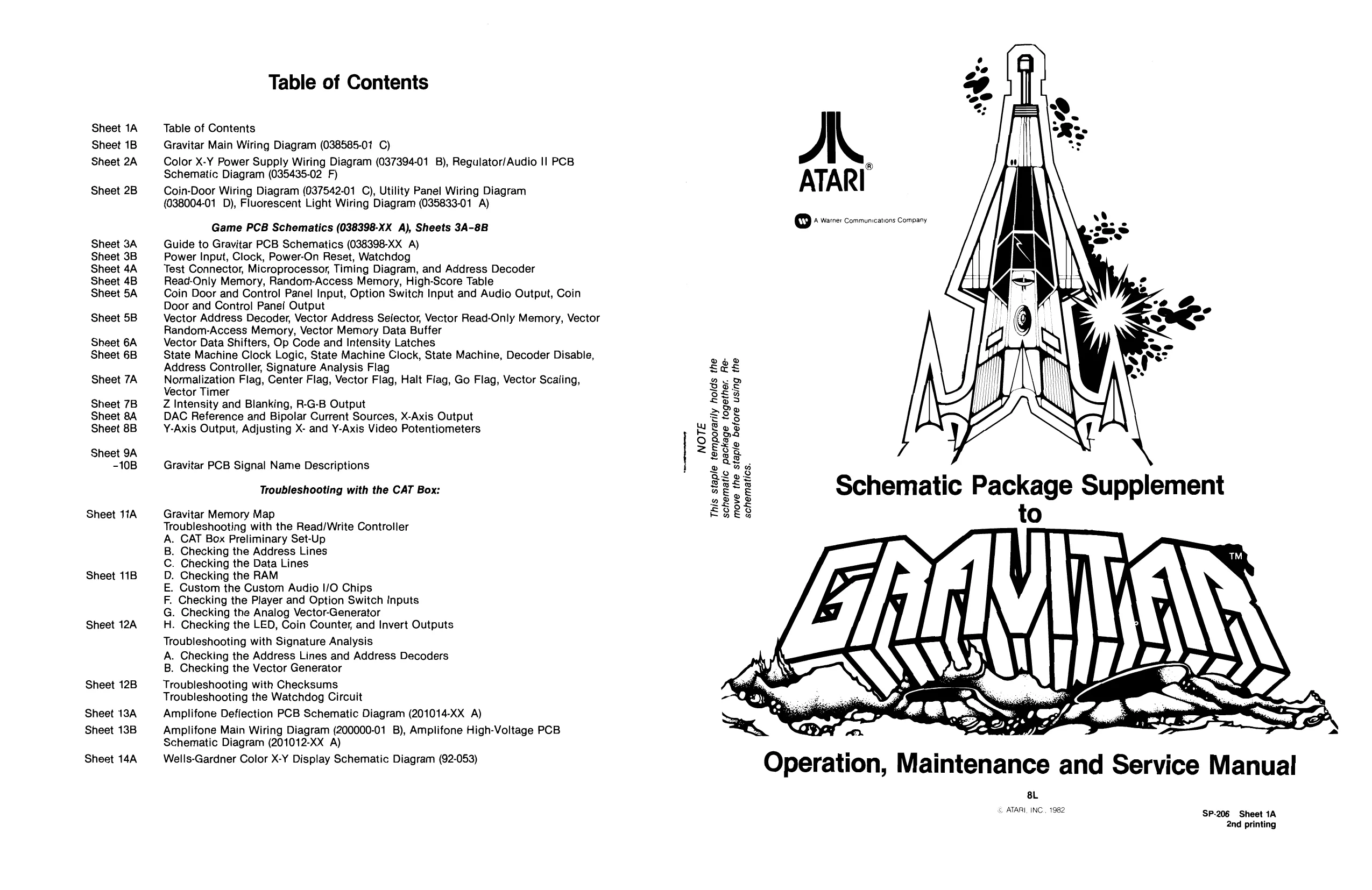
Table of Contents
Sheet 1A Table of Contents Sheet 1B Gravitar Main Wiring Diagram (038585-01 C) Sheet 2A Color X-Y Power Supply Wiring Diagram (037394-01 B), Regulator/Audio Il PCB ® Schematic Diagram (035435-02 F) ATARI Sheet 2B Coin-Door Wiring Diagram (037542-01 C), Utility Panel Wiring Diagram (038004-01 D), Fluorescent Light Wiring Diagram (035833-01 A) Game PCB Schematics (038398-XX A), Sheets 3A-8B + ver commncnsne conn
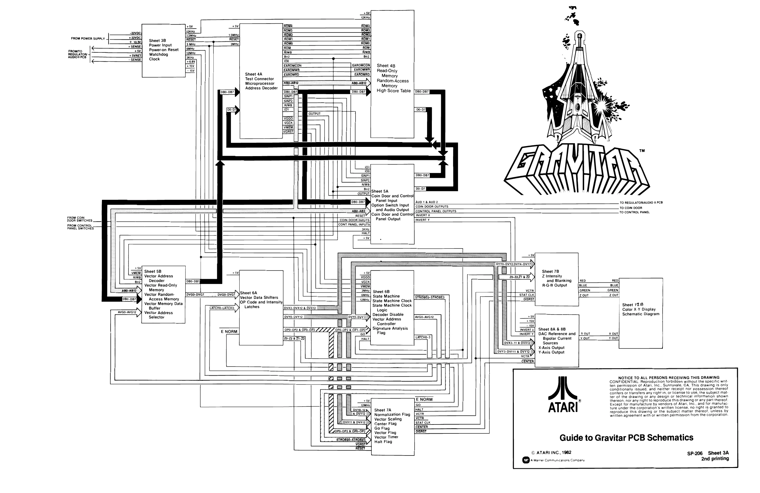
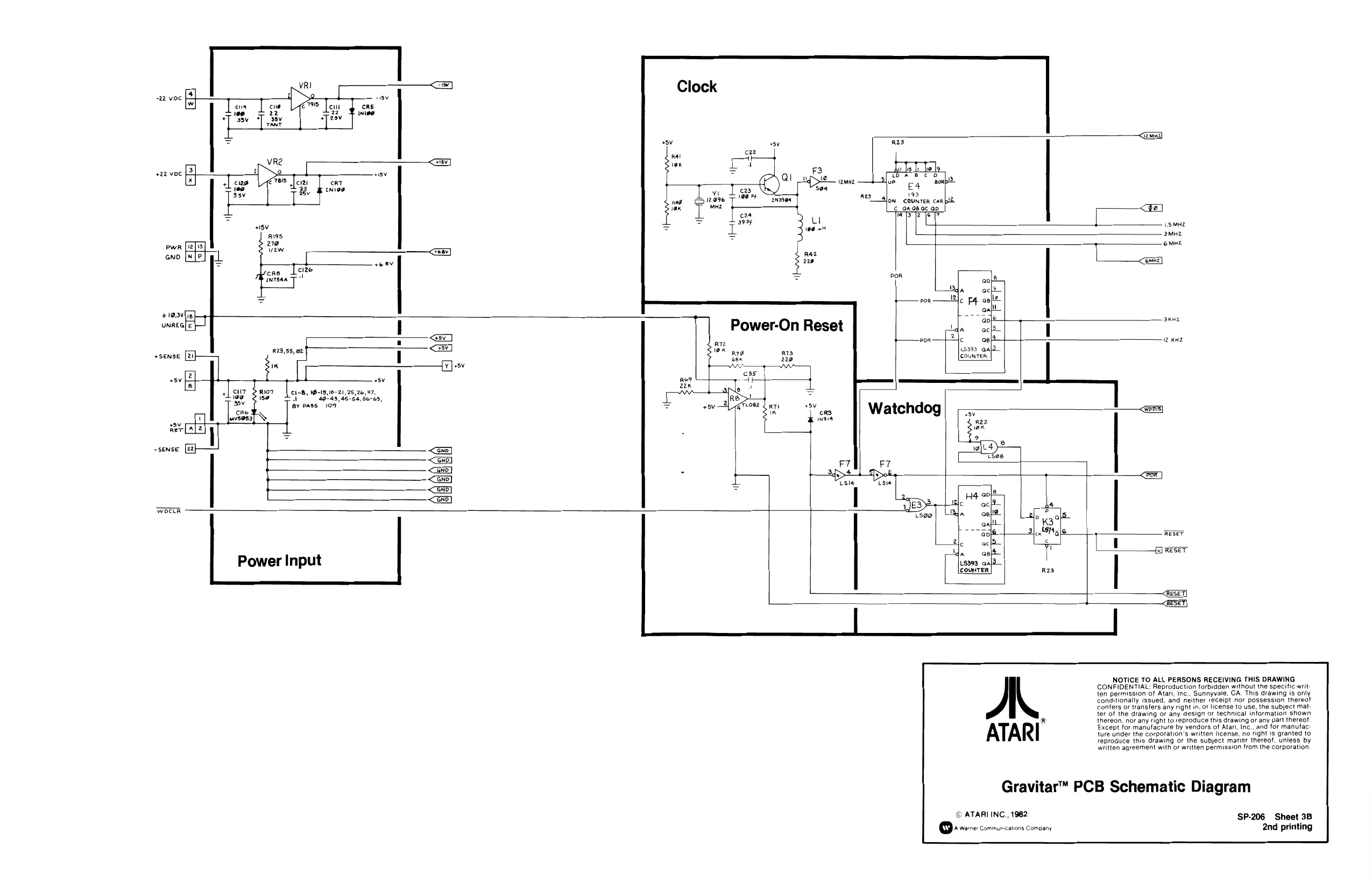
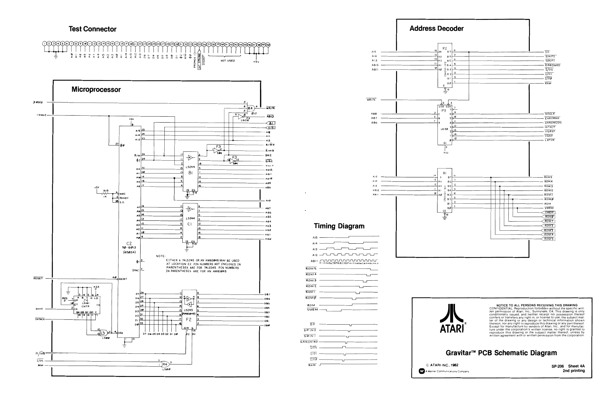
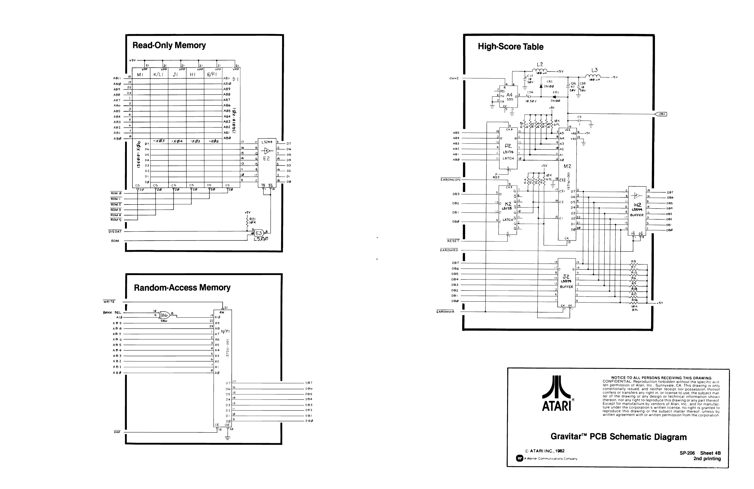
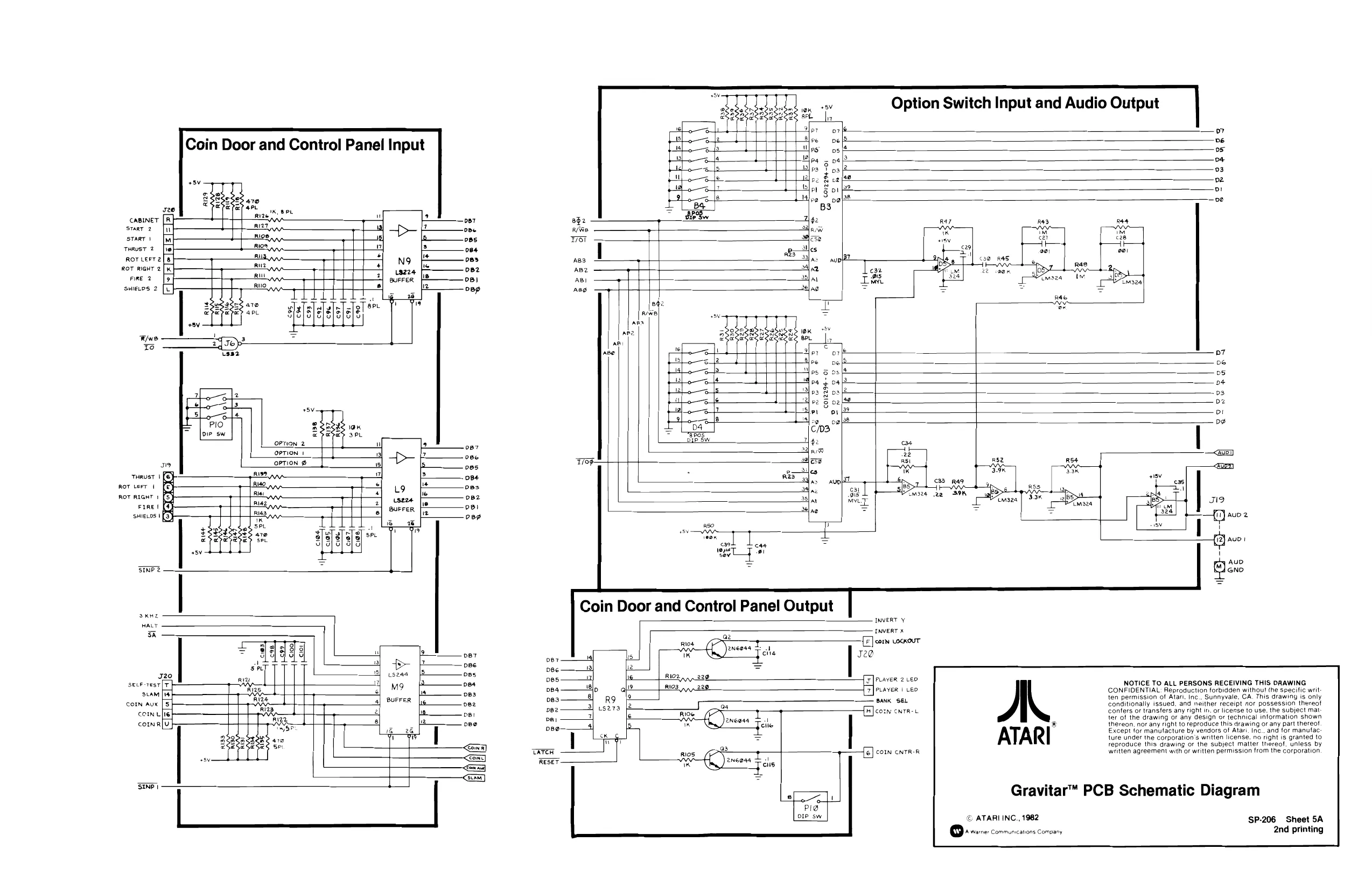
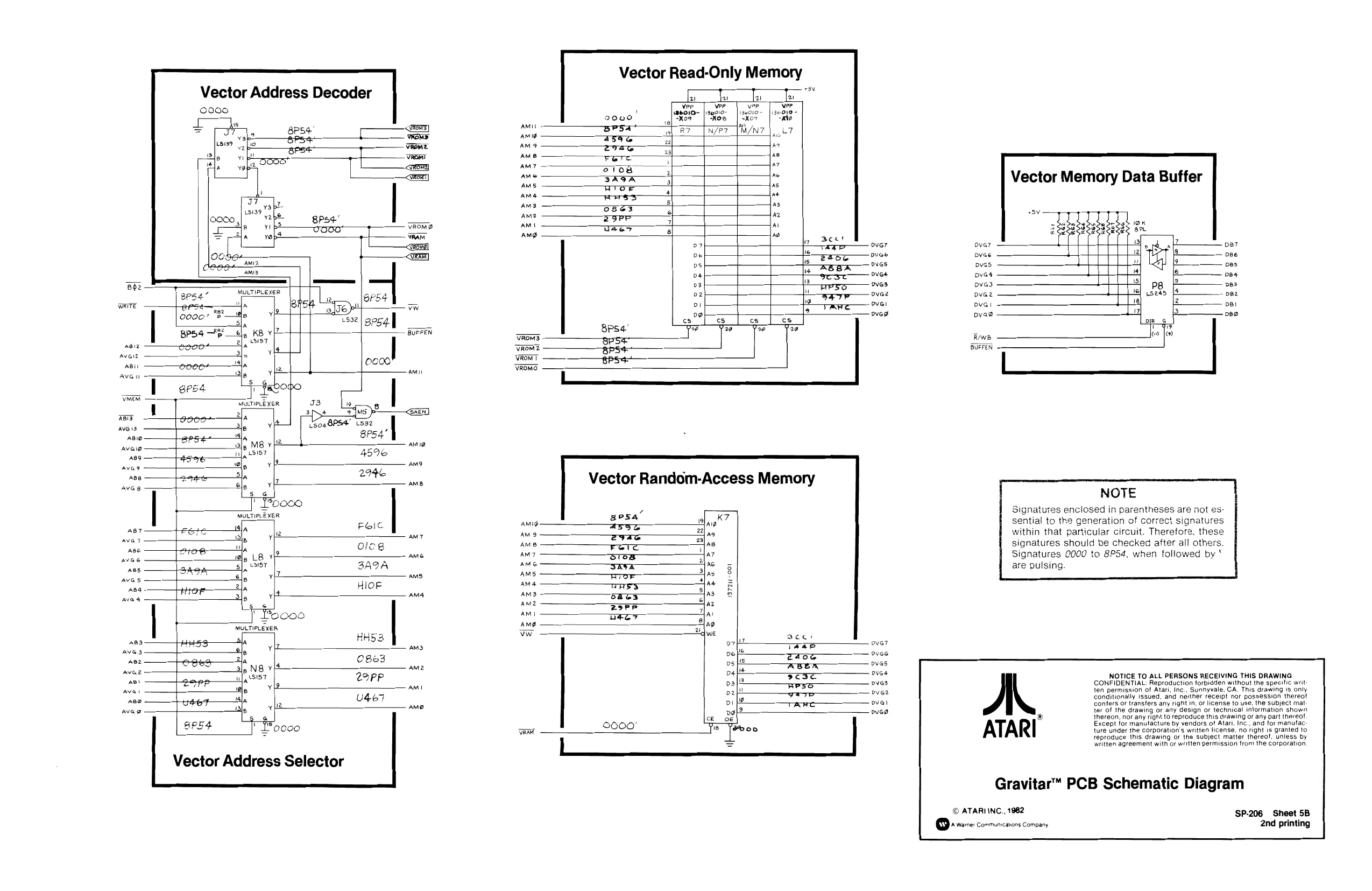
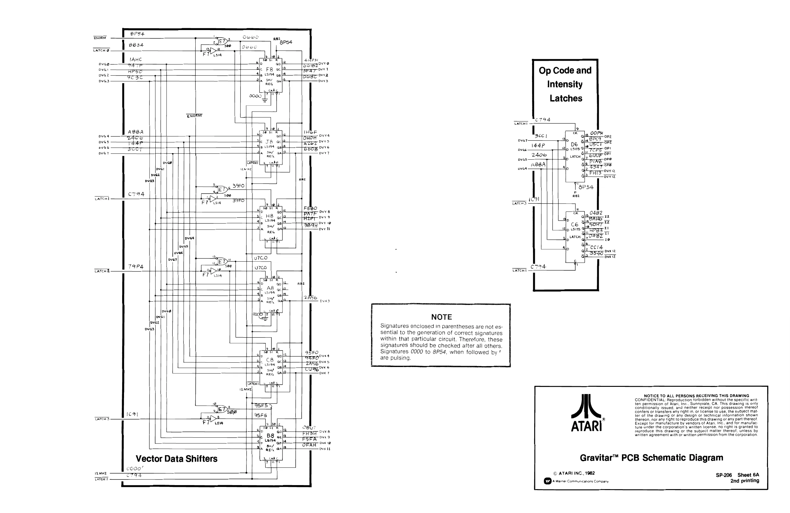
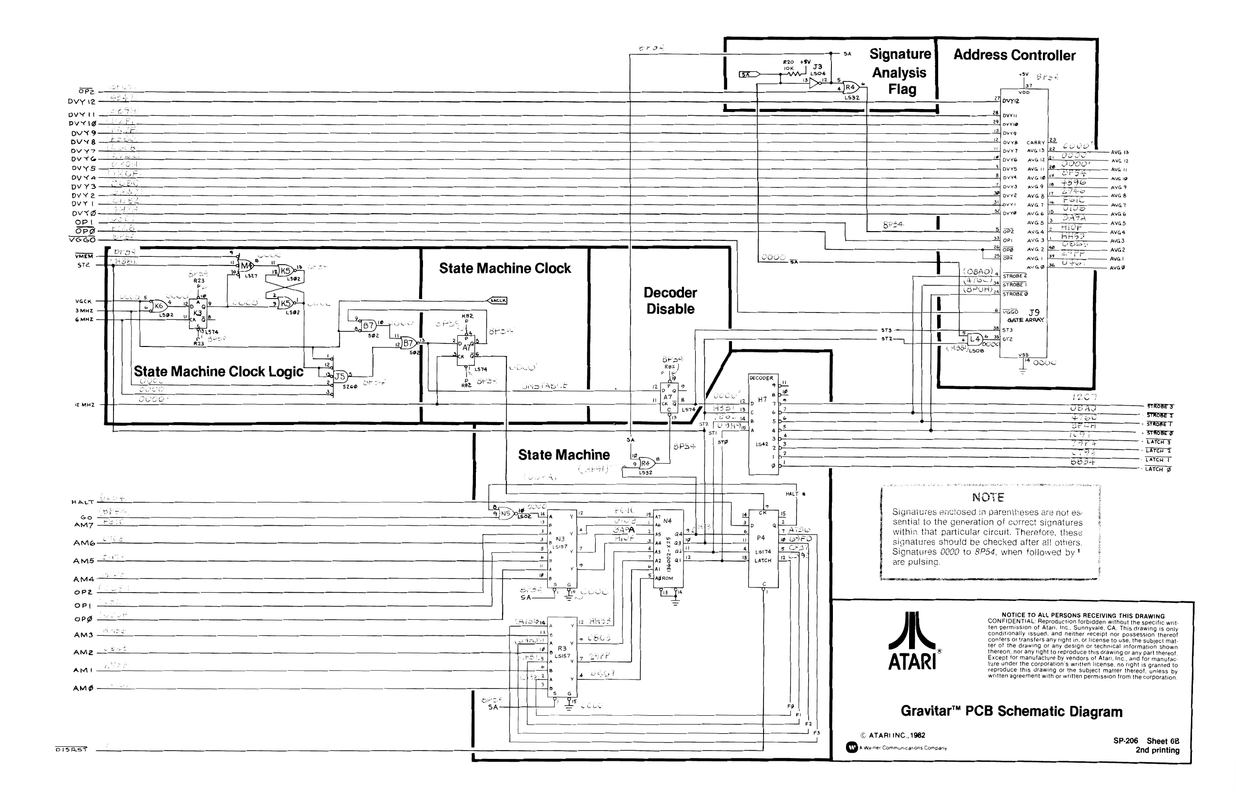
Sheet 3A Guide to Gravitar PCB Schematics (038398-XX A) Sheet 3B Power Input, Clock, Power-On Reset, Watchdog Sheet 4A Test Connector, Microprocessor, Timing Diagram, and Address Decoder Sheet 4B Read-Only Memory, Random-Access Memory, High-Score Table Sheet 5A Coin Door and Control Panel Input, Option Switch Input and Audio Output, Coin Door and Control Panel Output Sheet 5B Vector Address Decoder, Vector Address Selector, Vector Read-Only Memory, Vector Random-Access Memory, Vector Memory Data Buffer Sheet 6A Vector Data Shifters, Op Code and Intensity Latches Sheet 6B State Machine Clock Logic, State Machine Clock, State Machine, Decoder Disable, Address Controller, Signature Analysis Flag Sheet 7A Normalization Flag, Center Flag, Vector Flag, Halt Fiag, Go Flag, Vector Scaling, Vector Timer Sheet 7B Z Intensity and Blanking, R-G-B Output Sheet 8A DAC Reference and Bipolar Current Sources, X-Axis Output Sheet 8B Y-Axis Output, Adjusting X- and Y-Axis Video Potentiometers
Sheet 9A -10B Gravitar PCB Signal Name Descriptions
Troubleshooting with the CAT Box:
: Schematic Package Supplement E to Sheet 11A Gravitar Memory Map Troubleshooting with the Read/Write Controller A. CAT Box Preliminary Set-Up B. Checking the Address Lines C. Checking the Data Lines Sheet 11B D. Checking the RAM E. Custom the Custom Audio I/O Chips F. Checking the Player and Option Switch Inputs G. Checking the Analog Vector-Generator H. Checking the LED, Coin Counter, and Invert Outputs Troubleshooting with Signature Analysis A. Checking the Address Lines and Address Decoders B. Checking the Vector Generator Sheet 12B Troubleshooting with Checksums Troubleshooting the Watchdog Circuit Sheet 13A Amplifone Deflection PCB Schematic Diagram (201014-XX A) Sheet 13B Amplifone Main Wiring Diagram (200000-01 B), Amplifone High-Voltage PCB Schematic Diagram (201012-XX A) Sheet 14A Wells-Gardner Color X-Y Display Schematic Diagram (92-053) Operation, Maintenance and Service Manual
8L & ATARI, INC , 1982 Sheet 12A
SP.206 Sheet 1A
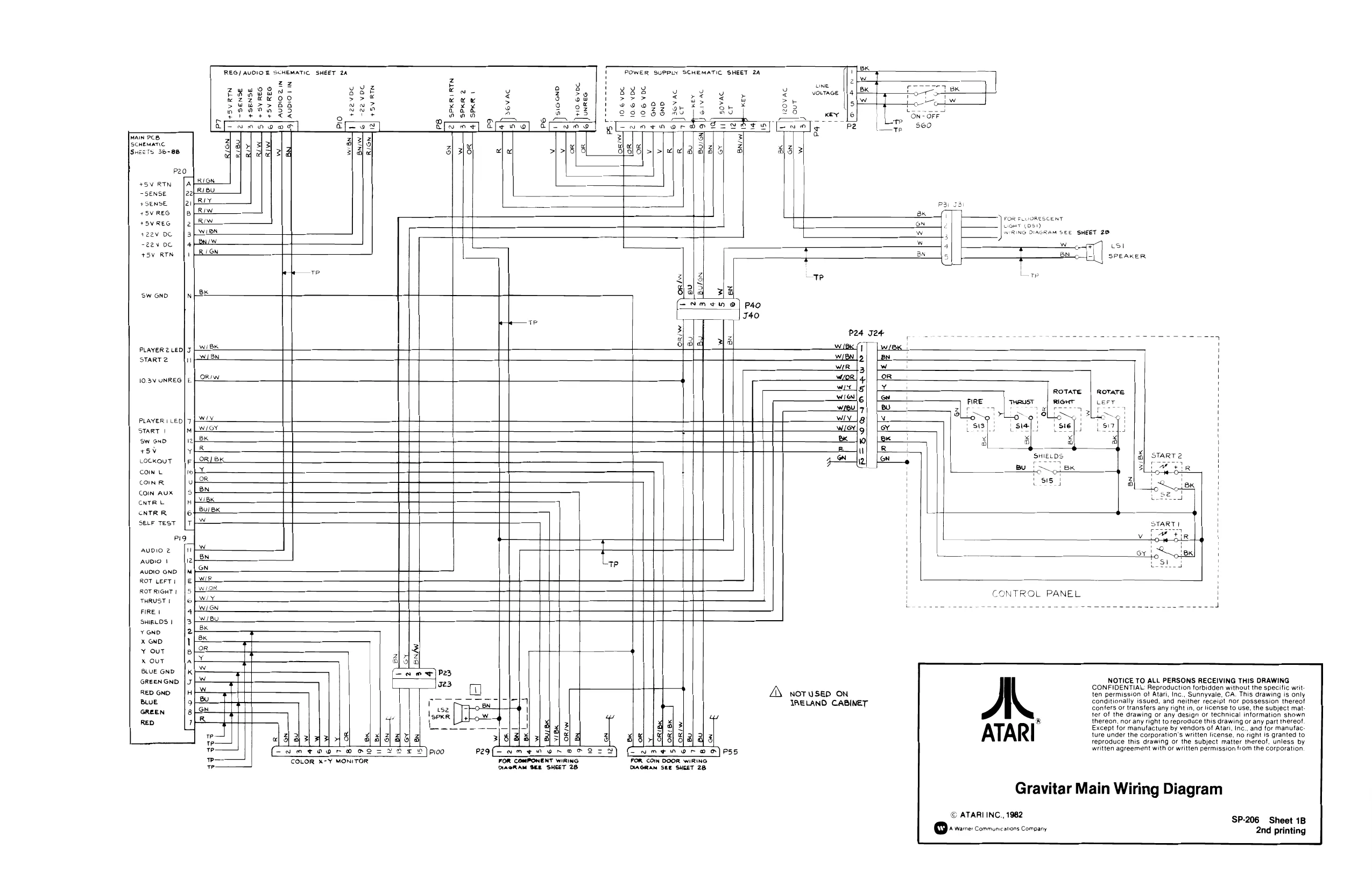
This page is a drawing, shown as the original scan.
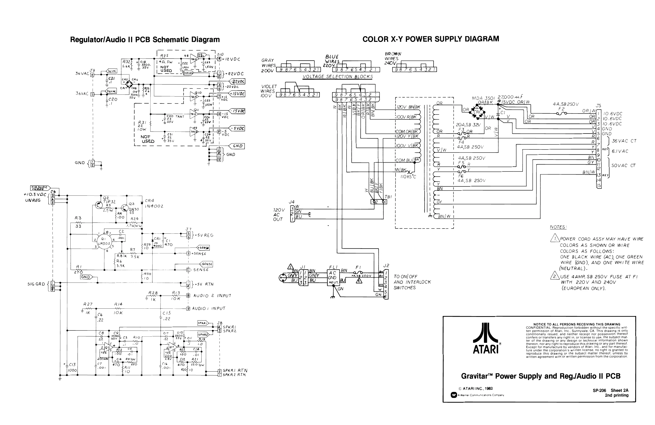
This page is a drawing, shown as the original scan.
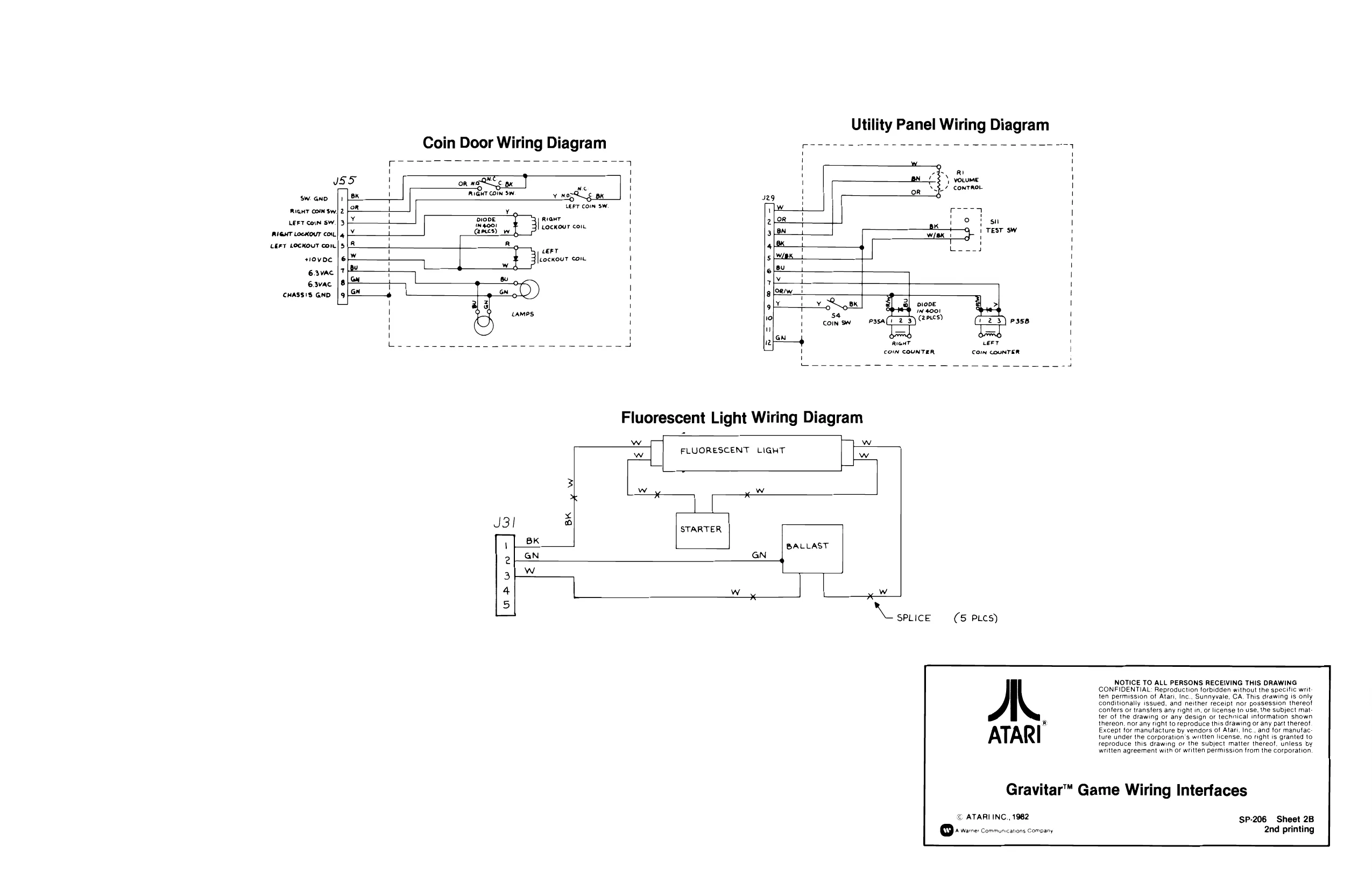
This page is a drawing, shown as the original scan.
This page is a drawing, shown as the original scan.
This page is a drawing, shown as the original scan.
This page is a drawing, shown as the original scan.
This page is a drawing, shown as the original scan.
This page is a drawing, shown as the original scan.
This page is a drawing, shown as the original scan.
Exon
aren.
ovao ova!
over Op Code and
pve3 5
Intensity
= Latches
[ENORT arent 9 he
| ; | ABBA | foe sR | IBGE og | copy | ||||
| ove | - | ~y | lo | aol | v | BCC I | al | H op2, |
| LACE | CROW | F | apca | |||||
| pves | mare | Ste JA ac | x | pvys | over | 3) | aa BPC? | |
| ° | 4}g U5194 | | | \44P | f | ||||
| REG | 2406 | q | ||||||
| CATCHY | oak | ayer | ||||||
| ne | ete | a8aA | q |
lover ene oves over! pvas, nee
C794 Soe
| TATE | C4 2 | srot+t— | ! |
| ci | |e bela | Tavens |
sear], FeO
| iD H | apy! | Ovye |
1, sean" 2a SM ate rt ted tana oves oves| . veT ba =. a r9P4 age 7 39.
| EE | [apse | . | care | 6204 |
FT “sia
age
ate L a oves
ves j
loves NOTE
jrvez it ote Signatures enciosed in parentheses are not essential to the generation of correct signatures within that particular circuit. Therefore, these a bel signatures should be checked after all others.
foe 95FO Signatures 0000 to 8P54, when followed by '
P cg 2 jens are pulsing.
| lc | ach | ZovKs |
Ye aie! opt OVE & su Sk la ae, Ape owt
TATCHT os ieee am vane NOTICE TO ALL PERSONS RECEIVING THIS DRAWING CONFIDENTIAL: Reproduction forbidden without the specific writ
12, TOBE ten permission of Atari, Inc.. Sunnyvale, CA. This drawing is only
> conditionally issued, and neither receipt nor possession thereof
| 1c | ce | SOP | Conters or transfers any nght in, or license to use, the subject mat | |
| = | od | 8 | 95F5 | ter of the drawing or any design or technical information shown |
| mS | 4 | ith rena ah ea | gi | gran oe |
| is | tole | Except for manufacture by vendors of Atari Inc.. and for manufac | ||
| fet | ey | our | ture under the corporation's written license. no fight is granted to | |
| jo | 00} | FHS | OVS | reproduce this drawing or the subject matter thereof, unless by |
| is | ia | written agreement with or written permission from the corporation |
'
., +3 STM . . Vector Data Shifters Gravitar™ PCB Schematic Diagram cooo’ veMnE CTS © ATARIING., 1982 Torr SP-206 Sheet 6A + W226" Communicanons Company 2nd printing
This page is a drawing, shown as the original scan.
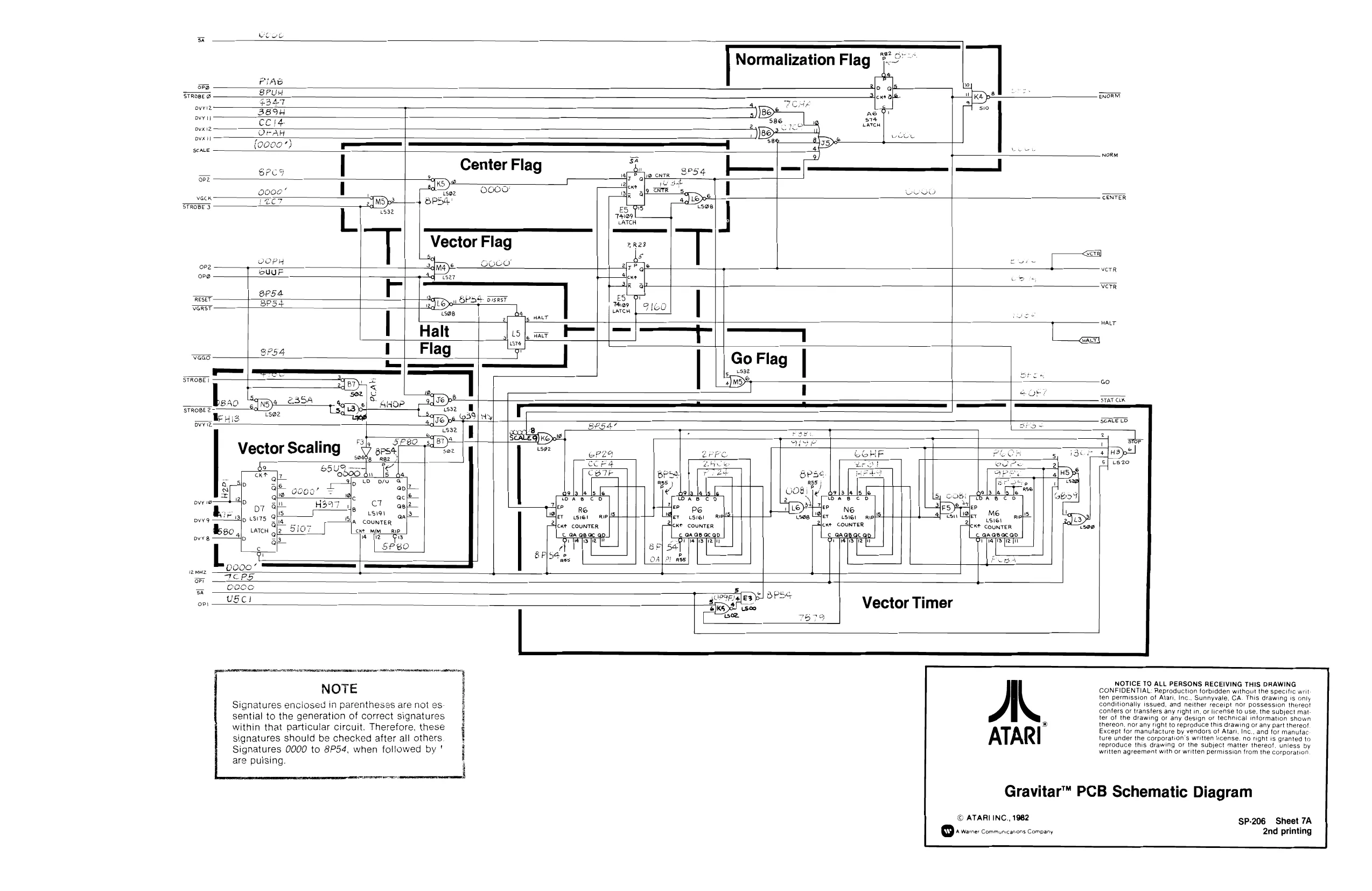
This page is a drawing, shown as the original scan.
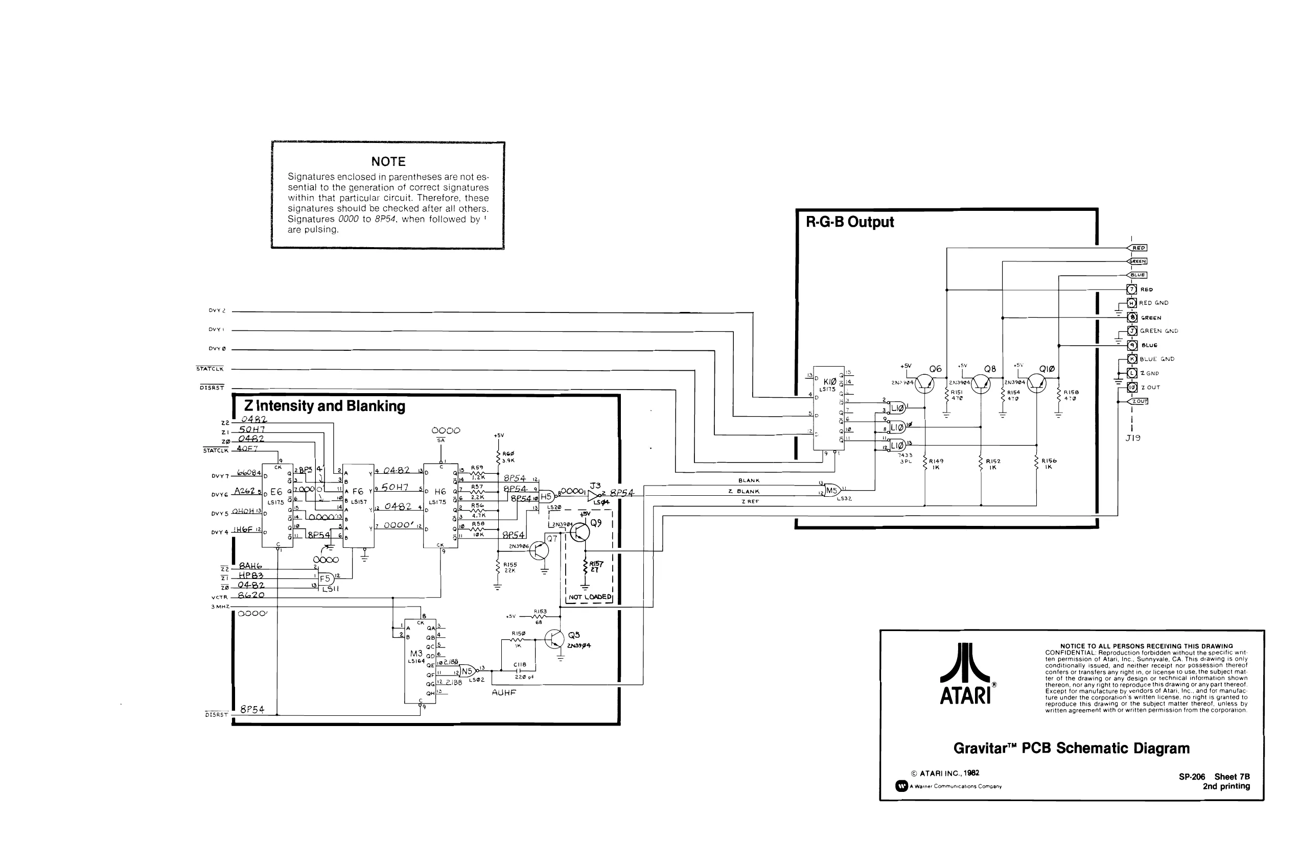
This page is a drawing, shown as the original scan.
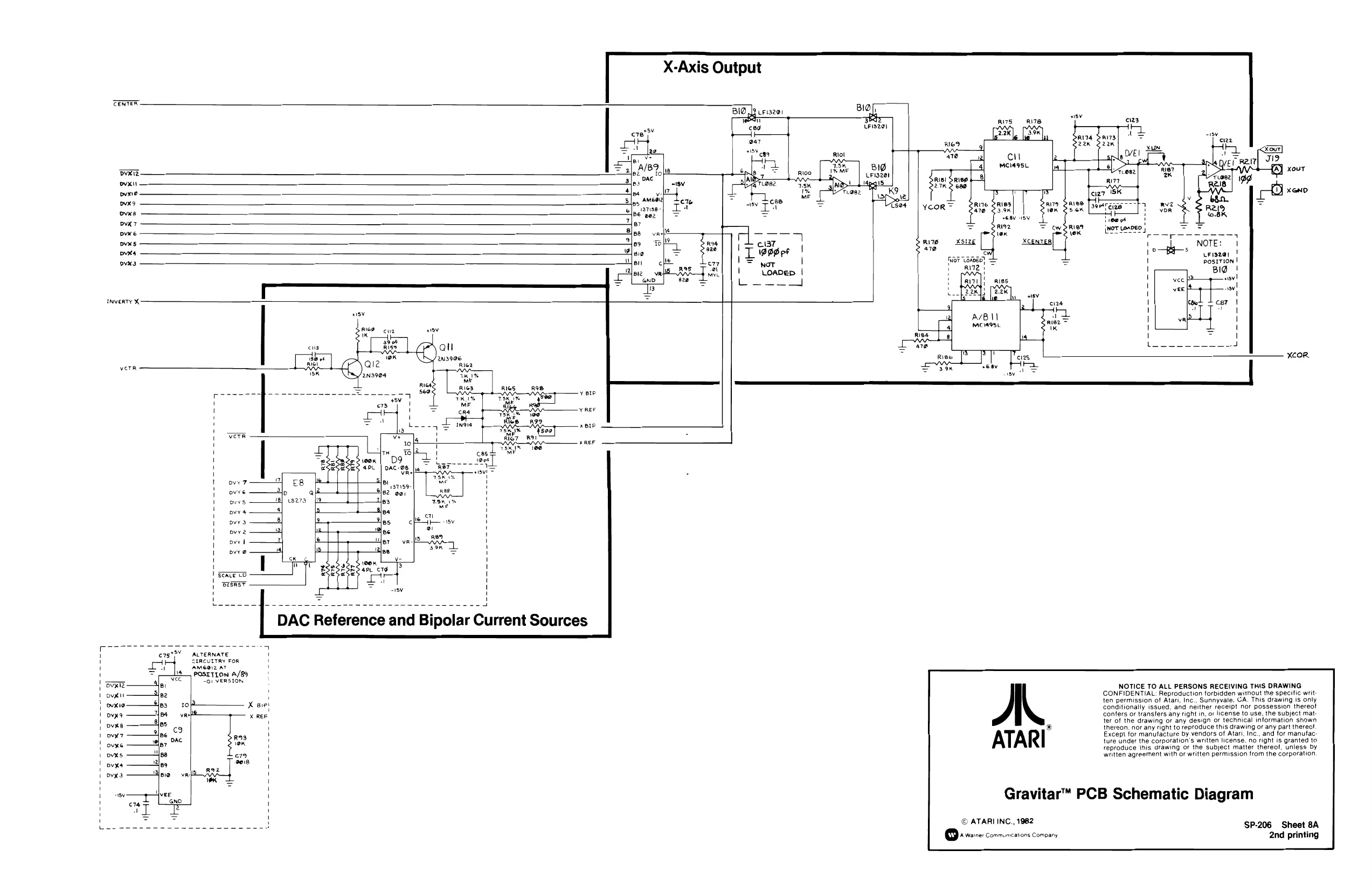
This page is a drawing, shown as the original scan.
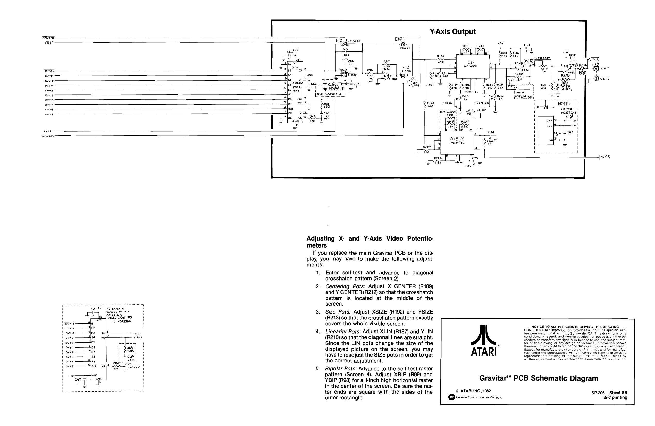
This page is a drawing, shown as the original scan.
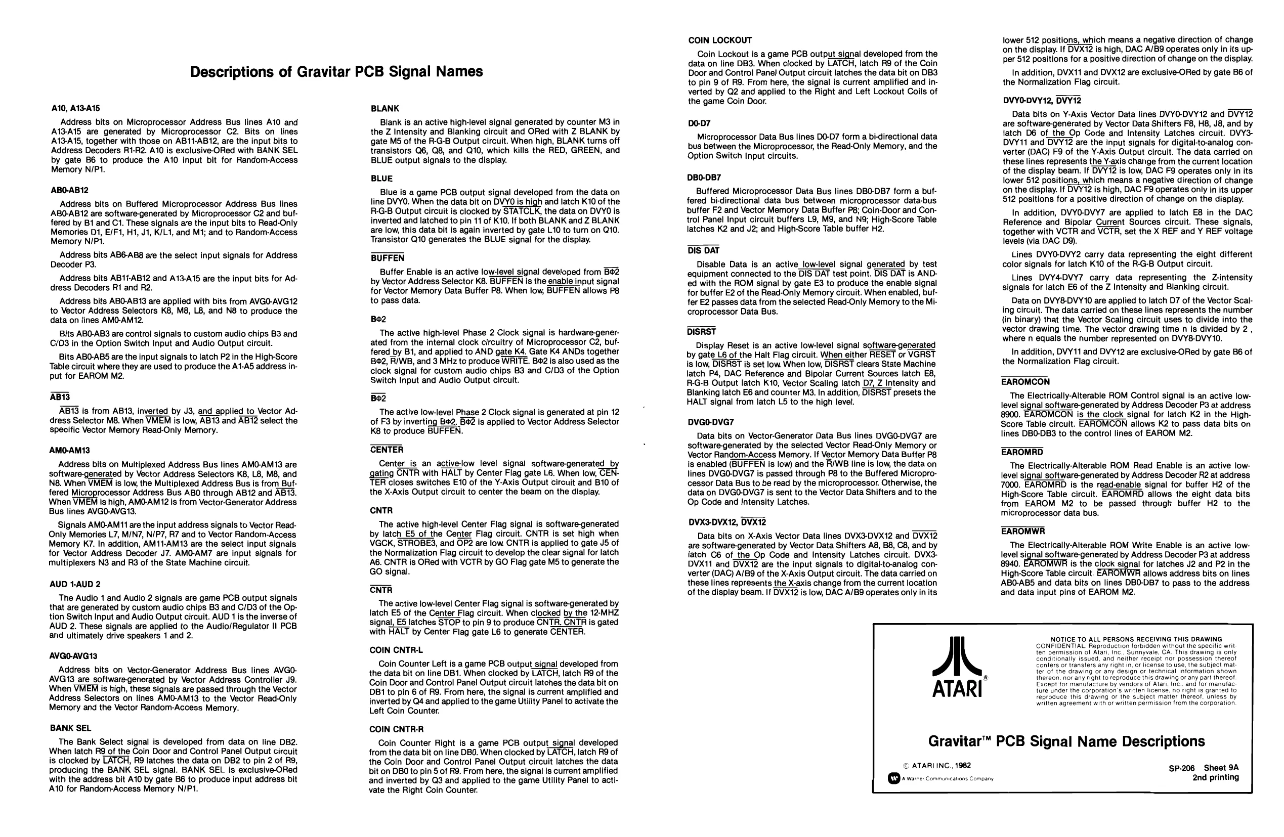
Descriptions of Gravitar PCB Signal Names
AM10, A13-A15 Address bits on Microprocessor Address Bus lines A10 and A13-A15 are generated by Microprocessor C2. Bits on lines A13-A15, together with those on AB11-AB12, are the input bits to Address Decoders R1-R2. A10 is exclusive-ORed with BANK SEL by gate B6 to produce the A10 input bit for Random-Access Memory N/P1.
ABO-AB12 Address bits on Buffered Microprocessor Address Bus lines AB0-AB12 are software-generated by Microprocessor C2 and buffered by B1 and C1. These signals are the input bits to Read-Only Memories 01, E/F1, H1, J1, K/L1, and M1; and to Random-Access Memory N/P1. Address bits AB6-AB8 are the select input signals for Address Decoder P3. Address bits AB17-AB12 and A13-A15 are the input bits for Address Decoders R1 and R2. Address bits ABO-AB13 are applied with bits from AVGO-AVG12 to Vector Address Selectors K8, M8, L8, and N8 to produce the data on lines AM0-AM12. Bits ABO-AB3 are control signals to custom audio chips B3 and C/D3 in the Option Switch Input and Audio Output circuit. Bits ABO-AB5 are the input signals to latch P2 in the High-Score Table circuit where they are used to produce the A1-A5 address input for EAROM M2.
ABTS KBiG is from AB13, inverted by J3, and applied to Vector Address Selector M8. When VMEM is low, AB13 and AB12 select the ‘specific Vector Memory Read-Only Memory.
AMO-AM13 Address bits on Multiplexed Address Bus lines AMO-AM13 are software-generated by Vector Address Selectors K8, L8, M8, and N8. When VMENM is low, the Multiplexed Address Bus is from Buffered Microprocessor Address Bus ABO through AB12 and AB13. When VMEN is high, AM0-AM12 is from Vector-Generator Address Bus lines AVGO-AVG13. Signals AMO-AM11 are the input address signals to Vector Read- Only Memories L7, M/N7, N/P7, R7 and to Vector Random-Access Memory K7. In addition, AM11-AM13 are the select input signals for Vector Address Decoder J7. AMO-AM7 are input signals for multiplexers N3 and R3 of the State Machine circuit.
AUD 1-AUD 2 The Audio 1 and Audio 2 signals are game PCB output signals that are generated by custom audio chips B3 and C/D3 of the Option Switch Input and Audio Output circuit. AUD 1 is the inverse of AUD 2. These signals are applied to the Audio/Regulator Il PCB and ultimately drive speakers 1 and 2.
AVGO-AVG13 Address bits on Vector-Generator Address Bus lines AVGO- AVG13 are software-generated by Vector Address Controller J9. When VMEM is high, these signals are passed through the Vector Address Selectors on lines AMO-AM13 to the Vector Read-Only Memory and the Vector Random-Access Memory.
BANK SEL The Bank Select signal is developed from data on line DB2. When latch R9 of the Coin Door and Control Panel Output circuit is clocked by LATCH, R9 latches the data on DB2 to pin 2 of R9, producing the BANK SEL signal. BANK SEL is exclusive-ORed with the address bit A10 by gate B6 to produce input address bit A10 for Random-Access Memory N/P1. BLANK Blank is an active high-level signal generated by counter M3 in the Z Intensity and Blanking circuit and ORed with Z BLANK by gate M5 of the R-G-B Output circuit. When high, BLANK turns off transistors Q6, Q8, and Q10, which kills the RED, GREEN, and BLUE output signals to the display.
BLUE Blue is a game PCB output signal developed from the data on line DVYO. When the data bit on DVY0 is high and latch K10 of the R-G-B Output circuit is clocked by STATCLK, the data on DVYO is inverted and latched to pin 11 of K10. If both BLANK and Z BLANK are low, this data bit is again inverted by gate 10 to turn on Q10. Transistor Q10 generates the BLUE signal for the display.
BUFFEN Buffer Enable is an active low-level signal developed from Bo2 by Vector Address Selector K8. BUFFEN is the enable input signal for Vector Memory Data Buffer P8. When low, BUFFEN allows P8 to pass data.
Bo2 The active high-level Phase 2 Clock signal is hardware-generated from the internal clock circuitry of Microprocessor C2, buffered by B1, and applied to AND gate K4. Gate K4 ANDs together B¢2, R/WB, and 3 MHz to produce WRITE. B92 is also used as the clock signal for custom audio chips B3 and C/D3 of the Option Switch Input and Audio Output circuit.
Bo2 The active low-level Phase 2 Clock signal is generated at pin 12
of F3 by inverting B®2, Bd2 is applied to Vector Address Selector
K8 to produce BUFFEN.
CENTER Center_is an active-low level signal software-generated_by gating CNTR with HALT by Center Flag gate L6. When low, CEN- TER closes switches E10 of the Y-Axis Output circuit and B10 of the X-Axis Output circuit to center the beam on the display.
CNTR The active high-level Center Flag signal is software-generated by latch E5 of the Center Flag circuit. CNTR is set high when VGCK, STROBES, and OP2 are low CNTR is applied to gate J5 of the Normalization Flag circuit to develop the clear signal for latch A6. CNTR is ORed with VCTR by GO Flag gate M5 to generate the GO signal.
CNTR The active low-level Center Flag signal is software-generated by latch ES of the Center Flag circuit. When clocked by the 12-MHZ signal, E5 latches STOP to pin 9 to produce CNTR. CNTR is gated with HALT by Center Flag gate L6 to generate CENTER.
COIN CNTR-L Coin Counter Left is a game PCB output signal developed from the data bit on line DB1. When clocked by LATCH, latch R9 of the Coin Door and Control Panel Output circuit latches the data bit on DB1 to pin 6 of R9. From here, the signal is current amplified and inverted by Q4 and applied to the game Utility Panel to activate the Left Coin Counter.
COIN CNTR-R Coin Counter Right is a game PCB output signal developed from the data bit on line DBO. When clocked by LATCH, latch R9 of the Coin Door and Control Panel Output circuit latches the data bit on DBO to pin 5 of R9. From here, the signal is current amplified and inverted by Q3 and applied to the game Utility Panel to activate the Right Coin Counter. COIN LOCKOUT Coin Lockout is a game PCB output signal developed from the data on line DB3. When clocked by LATCH, latch R9 of the Coin Door and Control Pane! Output circuit latches the data bit on DB3 to pin 9 of R9. From here, the signal is current amplified and inverted by Q2 and applied to the Right and Left Lockout Coils of the game Coin Door.
D0-D7 Microprocessor Data Bus lines D0-D7 form a bi-directional data bus between the Microprocessor, the Read-Only Memory, and the Option Switch Input circuits.
DBO-DB7 Buffered Microprocessor Data Bus lines DBO-DB7 form a buffered bi-directional data bus between microprocessor data-bus buffer F2 and Vector Memory Data Buffer P8; Coin-Door and Control Panel Input circuit buffers L9, M9, and N9; High-Score Table latches K2 and J2; and High-Score Table buffer H2.
DIS DAT Disable Data is an active low-level signal generated by test equipment connected to the DIS DAT test point. DIS DAT is ANDed with the ROM signal by gate E3 to produce the enable signal for buffer E2 of the Read-Only Memory circuit. When enabled, buffer E2 passes data from the selected Read-Only Memory to the Microprocessor Data Bus.
DISRST Display Reset is an active low-level signal software-generated by gate _L6 of the Halt Flag circuit. When either RESET or VGRST is low, DISRST is set low When low, DISRST clears State Machine latch P4, DAC Reference and Bipolar Current Sources latch E8, R-G-B Output latch K10, Vector Scaling latch D7, Z Intensity and Blanking latch E6 and counter M3. In addition, DISRST presets the HALT signal from latch L5 to the high level.
DVGO-DVG7 Data bits on Vector-Generator Data Bus lines DVGO-DVG7 are software-generated by the selected Vector Read-Only Memory or Vector Random-Access Memory. If Vector Memory Data Buffer P8 is enabled (BUFFEN is low) and the R/WB line is low, the data on lines DVGO-DVG7 is passed through P8 to the Buffered Microprocessor Data Bus to be read by the microprocessor. Otherwise, the data on DVGO-DVG7 is sent to the Vector Data Shifters and to the Op Code and !ntensity Latches.
DVX3-DVX12, DVX12 Data bits on X-Axis Vector Data lines DVX3-DVX12 and DVX12 are software-generated by Vector Data Shifters A8, B8, C8, and by latch C6 of_the Op Code and Intensity Latches circuit. DVX3- DVX11 and DVX12 are the input signals to digital-to-analog converter (DAC) A/B9 of the X-Axis Output circuit. The data carried on these lines represents the X-axis change from the current location of the display beam. If DVX12 is low, DAC A/B9 operates only in its
A.
ATARI
lower 512 positions, which means a negative direction of change ‘on the display. If DVX12 is high, DAC A/B9 operates only in its upper 512 positions for a positive direction of change on the display. In addition, DVX11 and DVX12 are exclusive-ORed by gate B6 of the Normalization Flag circuit.
DVYO-DVY12, DVY12 Data bits on Y-Axis Vector Data lines DVYO-DVY12 and DVY12 are software-generated by Vector Data Shifters F8, H8, J8, and by latch D6 of the Op Code and Intensity Latches circuit. DVY3- DVY11 and DVY12 are the input signals for digital-to-analog converter (DAC) F9 of the Y-Axis Output circuit. The data carried on these lines represents the Y-axis change from the current location of the display beam. If DVY12 is low, DAC F9 operates only in its lower 512 positions, which means a negative direction of change on the display. If DVY12 is high, DAC F9 operates only in its upper 512 positions for a positive direction of change on the display. In addition, DVYO-DVY7 are applied to latch E8 in the DAC Reference and Bipolar Current Sources circuit. These signals, together with VCTR and VCTR, set the X REF and Y REF voltage levels (via DAC D9). Lines DVYO-DVY2 carry data representing the eight different color signals for latch K10 of the R-G-B Output circuit. Lines DVY4-DVY7 carry data representing the Z-intensity signals for latch E6 of the Z Intensity and Blanking circuit. Data on DVY8-DVY10 are applied to latch D7 of the Vector Scaling circuit. The data carried on these lines represents the number (in binary) that the Vector Scaling circuit uses to divide into the vector drawing time. The vector drawing time n is divided by 2 , where n equals the number represented on DVY8-DVY10. In addition, DVY11 and DVY12 are exclusive-ORed by gate B6 of the Normalization Flag circuit.
EAROMCON The Electrically-Alterable ROM Control signal is an active lowlevel signal software-generated by Address Decoder P3 at address 8900. EAROMCON is the clock signal for latch K2 in the High- Score Table circuit. EAROMCON allows K2 to pass data bits on lines DBO-DB3 to the control lines of EAROM M2.
EAROMRD The Electrically-Alterable ROM Read Enable is an active lowlevel signal software-generated by Address Decoder R2 at address 7000. EAROMRD is the read-enable signal for buffer H2 of the High-Score Table circuit. EAROMRD allows the eight data bits from EAROM M2 to be passed through buffer H2 to the microprocessor data bus.
EAROMWR The Electrically-Alterable ROM Write Enable is an active lowlevel signal software-generated by Address Decoder P3 at address 8940. EAROMWR is the clock signal for latches J2 and P2 in the
High-Score Table circuit. EAROWWR allows address bits on lines
ABO-AB5 and data bits on lines DBO-DB7 to pass to the address and data input pins of EAROM M2.
NOTICE TO ALL PERSONS RECEIVING THIS DRAWING CONFIDENTIAL: Reproduction forbidden without the specific weit ten permission of Atari, Inc.. Sunnyvale, CA. This drawing is only conditionally issued, and neither receipt nor possession thereot Confers or transfers any right in, or license to use, the subject mat: ter of the drawing or any design or technical information shown
thereon. nor any right to reproduce this drawing or any part thereof
Except for manufacture by vendors of Atari, Inc., and for manufac. ture under the corporation's written license. no right is granted to reproduce this drawing or the subject matier thereof, unless by written agreement with or written permission from the corporation.
Gravitar™ PCB Signal Name Descriptions
© ATARI INC, 1982 SP-206 Sheet 9A
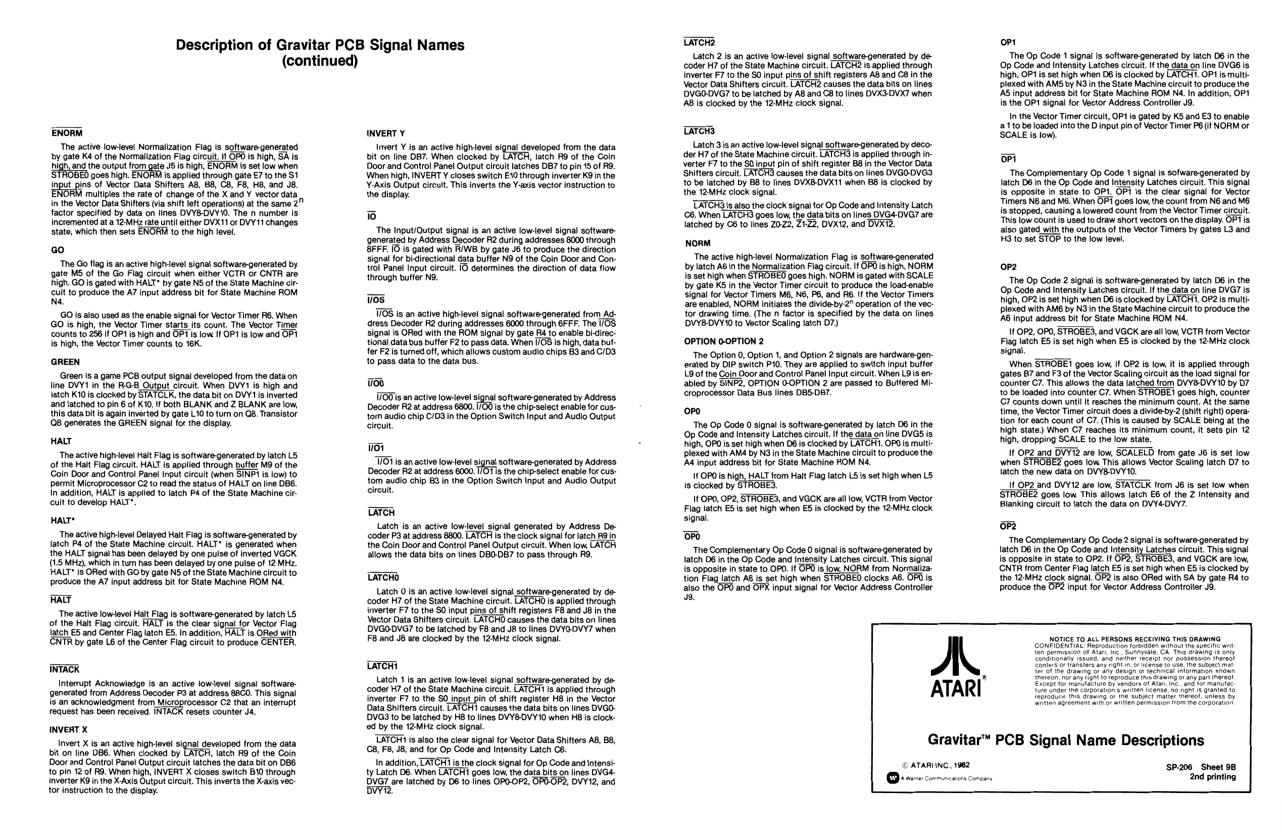
Description of Gravitar PCB Signal Names
(continued)
ENORM The active low-level Normalization Flag is software-generated by gate K4 of the Normalization Flag circuit. If OPO is high, SA is high, and the output from gate J5 is high, ENORM is set low when STROBEO goes high. ENORM is applied through gate £7 to the S1 input pins of Vector Data Shifters A8, B8, C8, F8, H8, and J8. NORM multiples the rate of change of the X and Y vector data in the Vector Data Shifters (via shift left operations) at the same 2 factor specified by data on lines DVY8-DVY10. The n number is incremented at a 12-MHz rate until either DVX11 or DVY11 changes state, which then sets ENORM to the high level.
Go The Go flag is an active high-level signal software-generated by gate M5 of the Go Flag circuit when either VCTR or CNTR are high. GO is gated with HALT* by gate N5 of the State Machine circuit to produce the A7 input address bit for State Machine ROM N4. GO is also used as the enable signal for Vector Timer R6. When GO is high, the Vector Timer starts its count. The Vector Timer counts to 256 if OP1 is high and OP1 is low If OP1 is low and OP1 is high, the Vector Timer counts to 16K.
GREEN Green is a game PCB output signal developed from the dataon line DVY1 in the R-G-B Output circuit. When DVY1 is high and latch K10 is clocked by STATCLK, the data bit on DVY1 is inverted and \atched to pin 6 of K10. !f both BLANK and Z BLANK are low, this data bit is again inverted by gate L10 to turn on Q8. Transistor Q8 generates the GREEN signal for the display.
HALT The active high-level Halt Flag is software-generated by latch L5 of the Halt Flag circuit. HALT is applied through buffer M9 of the Coin Door and Control Panel Input circuit (when SINP is low) to permit Microprocessor C2 to read the status of HALT on line DB6. In addition, HALT is applied to latch P4 of the State Machine circuit to develop HALT*.
HALT* The active high-level Delayed Halt Flag is software-generated by latch P4 of the State Machine circuit. HALT* is generated when the HALT signal has been delayed by one pulse of inverted VGCK (1.5 MHz), which in turn has been delayed by one pulse of 12 MHz. HALT* is ORed with GO by gate N5 of the State Machine circuit to produce the A7 input address bit for State Machine ROM N4.
HALT The active low-level Halt Flag is software-generated by latch L5 of the Halt Flag circuit. HALT is the clear signal for Vector Flag latch E5 and Center Flag latch E5. In addition, HALT is ORed with CNTR by gate L6 of the Center Flag circuit to produce CENTER.
INTACK Interrupt Acknowledge is an active low-level signal softwaregenerated from Address Decoder P3 at address 88C0. This signal is an acknowledgment from Microprocessor C2 that an interrupt request has been received. INTACK resets counter J4.
INVERT X Invert X is an active high-level signal developed from the data bit on line DB6. When clocked by LATCH, latch R9 of the Coin Door and Control Pane! Output circuit latches the data bit on DB6 to pin 12 of R9. When high, INVERT X closes switch B10 through inverter K9 in the X-Axis Output circuit. This inverts the X-axis vector instruction to the display. (INVERT Y Invert Y is an active high-level signal developed from the data bit on line DB7. When clocked by LATCH, latch R9 of the Coin Door and Control Panel Output circuit latches DB7 to pin 15 of R9.
When high, INVERT Y closes switch E10 through inverter K9 in the
Y-Axis Output circuit. This inverts the Y-axis vector instruction to the display.
The Input/Output signal is an active low-level signal softwaregenerated by Address Decoder R2 during addresses 8000 through 8FFF. [O is gated with R/WB by gate J6 to produce the direction signal for bi-directional data buffer N9 of the Coin Door and Control Panel Input circuit. iO determines the direction of data flow through buffer N9.
vos 1708 is an active high-level signal software-generated from Address Decoder R2 during addresses 6000 through 6FFF. The I/OS signal is ORed with the ROM signal by gate R4 to enable bi-directional data bus buffer F2 to pass data. When I/OS is high, data buffer F2 is turned off, which allows custom audio chips B3 and C/D3 to pass data to the data bus.
1/00 is an active low-level signal software-generated by Address Decoder R2 at address 6800. 1/00 is the chip-select enable for custom audio chip C/D3 in the Option Switch Input and Audio Output circuit.
1101 1/01 is an active low-level signal software-generated by Address Decoder R2 at address 6000. 1/OTis the chip-select enable for custom audio chip B3 in the Option Switch Input and Audio Output circuit.
LATCH Latch is an active low-level signal generated by Address De-
coder P3 at address 8800. LATCH is the clock signal for latch R9 in
the Coin Door and Control Panel Output circuit. When low, LATCH allows the data bits on lines DBO-DB7 to pass through R9.
LATCHO Latch 0 is an active low-level signal_software-generated by decoder H7 of the State Machine circuit. LATCHO is applied through inverter F7 to the SO input pins of shift registers F8 and J8 in the Vector Data Shifters circuit. LATCHO causes the data bits on lines DVGO0-DVG7 to be latched by F8 and J8 to lines DVY0-DVY7 when F8 and J8 are clocked by the 12-MHz clock signal.
LATCH1 Latch 1 is an active low-level signal_software-generated by decoder H7 of the State Machine circuit. LATCH1 is applied through
inverter F7 to the SO input pin of shift register H8 in the Vector
Data Shifters circuit. LATCH1 causes the data bits on lines DVGO- DVG3 to be latched by H8 to lines DVY8-DVY10 when H6 is clocked by the 12-MHz clock signal. LATCH1 is also the clear signal for Vector Data Shifters A8, B8, C8, F8, J8, and for Op Code and Intensity Latch C6. In addition, LATCH is the clock signal for Op Code and Intensity Latch D6. When LATCH? goes low, the data bits on lines DVG4- DVG7 are latched by D6 to lines OP0-OP2, OPO-OP2, DVY12, and Dvyi2. LATCH2 Latch 2 is an active low-level signal software-generated by de coder H7 of the State Machine circuit. LATCH2 is applied through inverter F7 to the SO input pins of shift registers A8 and C8 in the Vector Data Shifters circuit. LATCH2 causes the data bits on lines DVGO0-DVG7 to be latched by A8 and C8 to lines DVX3-DVX7 when AB is clocked by the 12-MHz clock signal.
LATCH3 Latch 3 is an active low-level signal software-generated by decoder H7 of the State Machine circuit. LATCHS is applied through inverter F7 to the S0 input pin of shift register B8 in the Vector Data Shifters circuit. 13 causes the data bits on lines DVGO-DVG3 to be latched by B8 to lines DVX8-DVX11 when B8 is clocked by the 12-MHz clock signal. LATCHS3is also the clock signal for Op Code and Intensity Latch C6. When LATCHS goes low, the data bits on lines DVG4-DVG7 are latched by C6 to lines Z0-22, 21-22, DVX12, and DVX12.
NORM The active high-level Normatization Flag is software-generated by latch A6 in the Normalization Fiag circuit. If OPO is high, NORM is set high when STROBEO goes high. NORM is gated with SCALE by gate K5 in the Vector Timer circuit to produce the load-enabie ‘signal for Vector Timers M6, N6, P6, and R6. If the Vector Timers are enabled, NORM initiates the divide-by-2” operation of the vector drawing time. (The n factor is specified by the data on lines DVY8-DVY10 to Vector Scaling latch D7.)
OPTION 0-OPTION 2 The Option 0, Option 1, and Option 2 signals are hardware-generated by DIP switch P10. They are applied to switch input buffer L9 of the Coin Door and Control Panel Input circuit. When L9 is enabled by SINP2, OPTION 0-OPTION 2 are passed to Buffered Microprocessor Data Bus lines DB5-DB7.
OPO The Op Code 0 signal is software-generated by latch D6 in the Op Code and Intensity Latches circuit. If the data on line DVGS is high, OPO is set high when D6 is clocked by LATCH1. OPO is multiplexed with AM4 by N3 in the State Machine circuit to produce the A4 input address bit for State Machine ROM N4. 1f OPO is high, HALT from Halt Flag latch L5 is set high when L5 is clocked by STROBES. If OPO, OP2, STROBES, and VGCK are all low, VCTR from Vector Flag latch E5 is set high when E5 is clocked by the 12-MHz clock signal.
OPO The Complementary Op Code 0 signal is software-generated by latch D6 in the Op Code and Intensity Latches circuit. This signal is opposite in state to OPO. If OPO is low, NORM from Normalization Flag latch A6 is set high when STROBEO clocks A6. OPO is also the OPO and OPX input signal for Vector Address Controller J3.
A. ATARI oP The Op Code 1 signal is software-generated by latch D6 in the Op Code and Intensity Latches circuit. If the data on line DVG6 is high, OP1 is set high when D6 is clocked by LATCH. OP1 is multiplexed with AMS5 by N3 in the State Machine circuit to produce the AS input address bit for State Machine ROM N4. In addition, OP1 is the OP1 signal for Vector Address Controller J9. In the Vector Timer circuit, OP1 is gated by K5 and E3 to enable a1 to be loaded into the D input pin of Vector Timer P6 (if NORM or SCALE is low).
OP1 The Complementary Op Code 1 signal is sofware-generated by latch D6 in the Op Code and Intensity Latches circuit. This signal is opposite in state to OP1. OP1 is the clear signal for Vector Timers N6 and M6. When OP1 goes low, the count from N6 and M6 is stopped, causing a lowered count from the Vector Timer circuit. This low count is used to draw short vectors on the display. OP1 is also gated with the outputs of the Vector Timers by gates L3 and H3 to set STOP to the low level.
OP2 The Op Code 2 signal is software-generated by latch D6 in the Op Code and Intensity Latches circuit. If the data on line DVG7 is high, OP2is set high when D6 is clocked by LATCH1. OP2 is multiplexed with AM6 by N@ in the State Machine circuit to produce the A6 input address bit for State Machine ROM N4. |f OP2, OPO, STROBE3, and VGCK are all low, VCTR from Vector Flag latch E5 is set high when E65 is clocked by the 12-MHz clock signal. When STROBE? goes low, if OP2 is low, it is applied through gates B7 and F3 of the Vector Scaling circuit as the load signal for counter C7. This allows the data latched from DVY8-DVY10 by D7 to be loaded into counter C7. When STROBE? goes high, counter C7 counts down until it reaches the minimum count. At the same time, the Vector Timer circuit does a divide-by-2 (shift right) operation for each count of C7. (This is caused by SCALE being at the high state.) When C7 reaches its minimum count, it sets pin 12 high, dropping SCALE to the low state. If OP2 and DVY12 are low, SCALELD from gate J6 is set low when STROBE2 goes low This allows Vector Scaling latch D7 to latch the new data on DVY8-DVY10. If OP2 and DVY12 are low, STATCLK from J6 is set low when STROBE2 goes low This allows latch E6 of the Z Intensity and Blanking circuit to latch the data on DVY4-DVY7.
OP2 The Complementary Op Code 2 signal is software-generated by latch D6 in the Op Code and Intensity Latches circuit. This signal is opposite in state to OP2. If OP2, STROBES, and VGCK are low, CNTR from Center Fiag latch E5 is set high when ES is clocked by the 12-MHz clock signal. OP2 is also ORed with SA by gate R4 to produce the OP2 input for Vector Address Controller J9.
NOTICE TO ALL PERSONS RECEIVING THIS DRAWING CONFIDENTIAL: Reproduction forbidden without the specific writ: ten permission of Atari, inc., Sunnyvale, CA. This drawing is only conditionally issued, and neither receipt nor possession thereof Conters or transfers any right in, or license to use, the subject mat ter of the drawing or any design or technical information shown thereon. nor any right to reproduce this drawing or any part thereo!. Except for manutacture by vendors of Ata, Inc., and for manufac: ture under the corporation's written license, no right is granted to reproduce this drawing or the subject matter thereof, unless by written agreement with or written permission (rom the corporation.
Gravitar™ PCB Signal Name Descriptions
© ATARIANC., 1982 SP.206 Sheet 9B
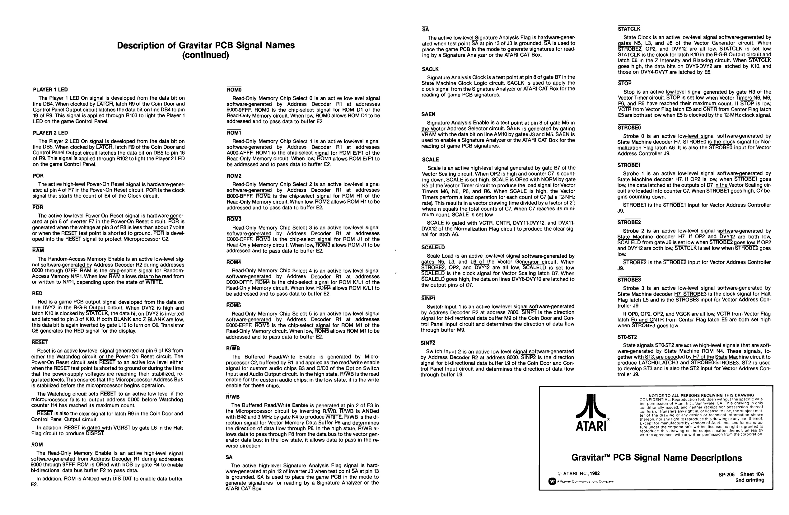
Description of Gravitar PCB Signal Names
(continued)
PLAYER 1 LED The Player 1 LED On signal is developed from the data bit on line DB4. When clocked by LATCH, latch R9 of the Coin Door and Control Panel Output circuit latches the data bit on line DB4 to pin 19 of R9. This signal is applied through R103 to light the Player 1 LED on the game Control Panel.
PLAYER 2 LED The Player 2 LED On signal is developed from the data bit on line DBS. When clocked by LATCH, latch R9 of the Coin Door and Control Panel Output circuit latches the data bit on DBS to pin 16 of R9. This signal is applied through R102 to light the Player 2 LED on the game Control Panel,
POR The active high-level Power-On Reset signal is hardware-generated at pin 4 of F7 in the Power-On Reset circuit. POR is the clock signal that starts the count of E4 of the Clock circuit.
POR The active low-level Power-On Reset signal is hardware-generated at pin 6 of inverter F7 in the Power-On Reset circuit. POR is generated when the voltage at pin 3 of R8 is less than about 7 volts or when the RESET test point is shorted to ground. POR is developed into the RESET signal to protect Microprocessor C2.
RAM The Random-Access Memory Enable is an active low-level signal software-generated by Address Decoder R2 during addresses 0000 through 07FF. RAM is the chip-enable signal for Random- Access Memory N/P1. When low, RAM allows data to be read from cor written to N/P1, depending upon the state of WRITE.
RED Red is a game PCB output signal developed from the data on line DVY2 in the R-G-B Output circuit. When DVY2 is high and latch K10 is clocked by STATCLK, the data bit on DVY2 is inverted and latched to pin 3 of K10. If both BLANK and Z BLANK are low, this data bit is again inverted by gate L10 to turn on Q6. Transistor Q6 generates the RED signal for the display.
RESET Reset is an active low-level signal generated at pin 6 of K3 from either the Watchdog circuit or the Power-On Reset circuit. The Power-On Reset circuit sets RESET to an active low level either when the RESET test point is shorted to ground or during the time that the power-supply voltages are reaching their stabilized, regu-lated levels. This ensures that the Microprocessor Address Bus is stabilized before the microprocessor begins operation. The Watchdog circuit sets RESET to an active low level if the microprocessor fails to output address 0D00 before Watchdog counter H4 has reached its maximum count. RESET is also the clear signal for latch R9 in the Coin Door and Control Panel Output circuit. In addition, RESET is gated with VGRST by gate L6 in the Halt Flag circuit to produce DISRST.
ROM The Read-Only Memory Enable is an active high-level signal software-generated from Address Decoder R1 during addresses 9000 through 9FFF. ROM is ORed with I/OS by gate R4 to enable bi-directional data bus buffer F2 to pass data. In addition, ROM is ANDed with DIS DAT to enable data buffer ROMO Read-Only Memory Chip Select 0 is an active low-level signal software-generated by Address Decoder R1 at addresses 9000-9F FF. ROMO is the chip-select signal for ROM D1 of the Read-Only Memory circuit. When low, ROMO allows ROM D1 to be addressed and to pass data to buffer E2.
ROM1 Read-Only Memory Chip Select 1 is an active low-level signal software-generated by Address Decoder R1 at addresses A000-AFFF. ROM1 is the chip-select signal for ROM E/F1 of the Read-Only Memory circuit. When low, ROM1 aliows ROM E/F1 to be addressed and to pass data to buffer E2.
ROM2 Read-Only Memory Chip Select 2 is an active low-level signal software-generated by Address Decoder R1 at addresses B000-BFFF. ROM2 is the chip-select signal for ROM H1 of the Read-Only Memory circuit. When low, allows ROM H1 to be addressed and to pass data to buffer E2.
ROM3 Read-Only Memory Chip Select 3 is an active low-level signal software-generated by Address Decoder R1 at addresses C000-CFFF. ROMS is the chip-select_signal for ROM J1 of the
Read-Only Memory circuit. When low, ROM3 allows ROM J1 to be
addressed and to pass data to buffer E2.
ROM4 Read-Only Memory Chip Select 4 is an active low-level signal software-generated by Address Decoder R1 at addresses DO00-DFFF. ROM4 is the chip-select signal for ROM K/L1 of the Read-Only Memory circuit. When low, ROM4 allows ROM K/L1 to be addressed and to pass data to buffer E2.
ROMS: Read-Only Memory Chip Select 5 is an active low-level signal software-generated by Address Decoder R1 at addresses E000-EFFF. ROMS is the chip-select signal for ROM M1 of the Read-Only Memory circuit. When low, ROMS allows ROM M1 to be addressed and to pass data to buffer E2.
RIWB The Buffered Read/Write Enable is generated by Microprocessor C2, buffered by B1, and applied as the read/write enable signal for custom audio chips B3 and C/D3 of the Option Switch Input and Audio Output circuit. In the high state, R/WB is the read enable for the custom audio chips; in the low state, it is the write enable for these chips.
RWB The Buffered Read/Write Eanble is generated at pin 2 of F3 in the Microprocessor circuit by inverting R/WB. R/WB is ANDed with B2 and 3 MHz by gate K4 to produce WRITE. R/WB is the direction signal for Vector Memory Data Buffer P8 and determines the direction of data flow through P8. In the high state, R/WB allows data to pass through P8 from the data bus to the vector generator data bus; in the low state, it allows data to pass in the reverse direction.
SA The active high-level Signature Analysis Flag signal is hardware-generated at pin 12 of inverter J3 when test point SA at pin 13 is grounded. SA is used to place the game PCB in the mode to generate signatures for reading by a Signature Analyzer or the ATARI CAT Box. SA The active low-level Signature Analysis Flag is hardware-generated when test point SA at pin 13 of J3 is grounded. SA is used to place the game PCB in the mode to generate signatures for reading by a Signature Analyzer or the ATARI CAT Box.
SACLK Signature Analysis Clock is a test point at pin 8 of gate B7 in the State Machine Clock Logic circuit. SACLK is used to apply the clock signal from the Signature Analyzer or ATARI CAT Box for the reading of game PCB signatures.
SAEN Signature Analysis Enable is a test point at pin 8 of gate M5 in the Vector Address Selector circuit. SAEN is generated by gating VRAM with the data bit on line AM10 by gates J3 and M5. SAEN is used to enable a Signature Analyzer or the ATARI CAT Box for the reading of game PCB signatures.
SCALE Scale is an active high-level signal generated by gate B7 of the Vector Scaling circuit. When OP2 is high and counter C7 is counting down, SCALE is set high. SCALE is ORed with NORM by gate K5 of the Vector Timer circuit to produce the load signal for Vector Timers M6, N6, P6, and R6. When SCALE is high, the Vector Timers perform a load operation for each count of C7 (at a 12-NHz rate). This results in a vector drawing time divided by a factor of 2", where n equals the total counts of C7. When C7 reaches its minimum count, SCALE is set low. SCALE is gated with VCTR, CNTR, DVY11-DVY12, and DVX11- DVX12 of the Normalization Flag circuit to produce the clear signal for latch A6.
SCALELD Scale Load is an active low-level signal software-generated by gates NS, L3, and L6_of the Vector Generator circuit. When STROBE2, OP2, and DVY12 are all low, SCALELD is set low SCALELD is the clock signal for Vector Scaling latch D7. When SCALELD goes high, the data on lines DVY8-DVY10 are latched to the output pins of 07.
‘SINP1 Switch Input 1 is an active low-level signal software-generated by Address Decoder R2 at address 7800. SINP1 is the direction signal for bi-directional data buffer M9 of the Coin Door and Control Panel Input circuit and determines the direction of data flow through buffer M9.
‘SINP2 Switch Input 2 is an active low-level signal software-generated by Address Decoder R2 at address 8000. SINP2 is the direction signal for bi-directional data buffer L9 of the Coin Door and Control Panel Input circuit and determines the direction of data flow through buffer L9.
A, STATCLK State Clock is an active low-level signal software-generated by gates N5, L3, and J6 of the Vector Generator circuit. When STROBE2, OP2, and DVY12 are all low, STATCLK is set low ‘STATCLK is the clock for latch K10 in the R-G-B Output circuit and latch E6 in the Z Intensity and Blanking circuit. When STATCLK goes high, the data bits on DVYO-DVY2 are latched by K10, and those on DVY4-DVY7 are latched by E6.
STOP Stop is an active low-level signal generated by gate H3 of the Vector Timer circuit. STOP is set low when Vector Timers N6, M6, P6, and R6 have reached their maximum count. If STOP is low, VCTR from Vector Flag latch E5 and CNTR from Center Flag latch ES are both set low when ES is clocked by the 12-MHz clock signal.
STROBEO Strobe 0 is an active low-level signal software-generated by State Machine decoder H7. STROBEO is the clock signal for Normalization Flag latch A6. It is also the STROBEO input for Vector Address Controller J9.
STROBE1 Strobe 1 is an active low-level signal software-generated by State Machine decoder H7. If OP2 is low, when STROBE1 goes low, the data latched at the outputs of D7 in the Vector Scaling circuit are loaded into counter C7. When STROBE1 goes high, C7 begins counting down. STROBE1 is the STROBE1 input for Vector Address Controller J9.
STROBE2 Strobe 2 is an active low-level signal software-generated by
State Machine decoder H7. If OP2 and DVY12 are both low,
SCALELD from gate J6 is set low when STROBE2 goes low If OP2 and DVY12 are both low, STATCLK is set low when STROBE2 goes. low STROBE2 is the STROBE2 input for Vector Address Controller 19. J
STROBES Strobe 3 is an active low-level_signal software-generated by State Machine decoder H7. STROBES is the clock signal for Halt Flag latch L5 and is the STROBES input for Vector Address Controller J9. If OPO, OP2, OP2, and VGCK are all low, VOTR from Vector Flag latch E5 and CNTR from Center Flag latch E5 are both set high when STROBES goes low
STO-ST2 State signals STO-ST2 are active high-level signals that are software-generated by State Machine ROM N4. These signals, together with ST3, are decoded by H7 of the State Machine circuit to produce LATCHO-LATCH3 and STROBEO-STROBES. ST2 is used to develop ST3 and is also the ST2 input for Vector Address Controller J9.
NOTICE TO ALL PERSONS RECEIVING THIS DRAWING
CONFIDENTIAL: Reproduction forbidden without the specific writ: Confers or transfers any right in, or license to use, the subject mat:
ten permission of Atari, Inc, Sunnyvale. CA. This drawing is only Conditionally issued, and neither receipt nor possession thereot
ter of the drawing or any design or technical information shown
thereon. nor any right to reproduce this drawing or any part thereo!
Except for manufacture by vendors of Atari, Inc., and for manufac: ture Under the corporation's written license, no right is granted to reproduce this drawing or the subject matter thereof, unless by written agreement with or written permission from the corporation.
Gravitar™ PCB Signal Name Descriptions
© ATARI INC., 1982 SP-206 Sheet 10A
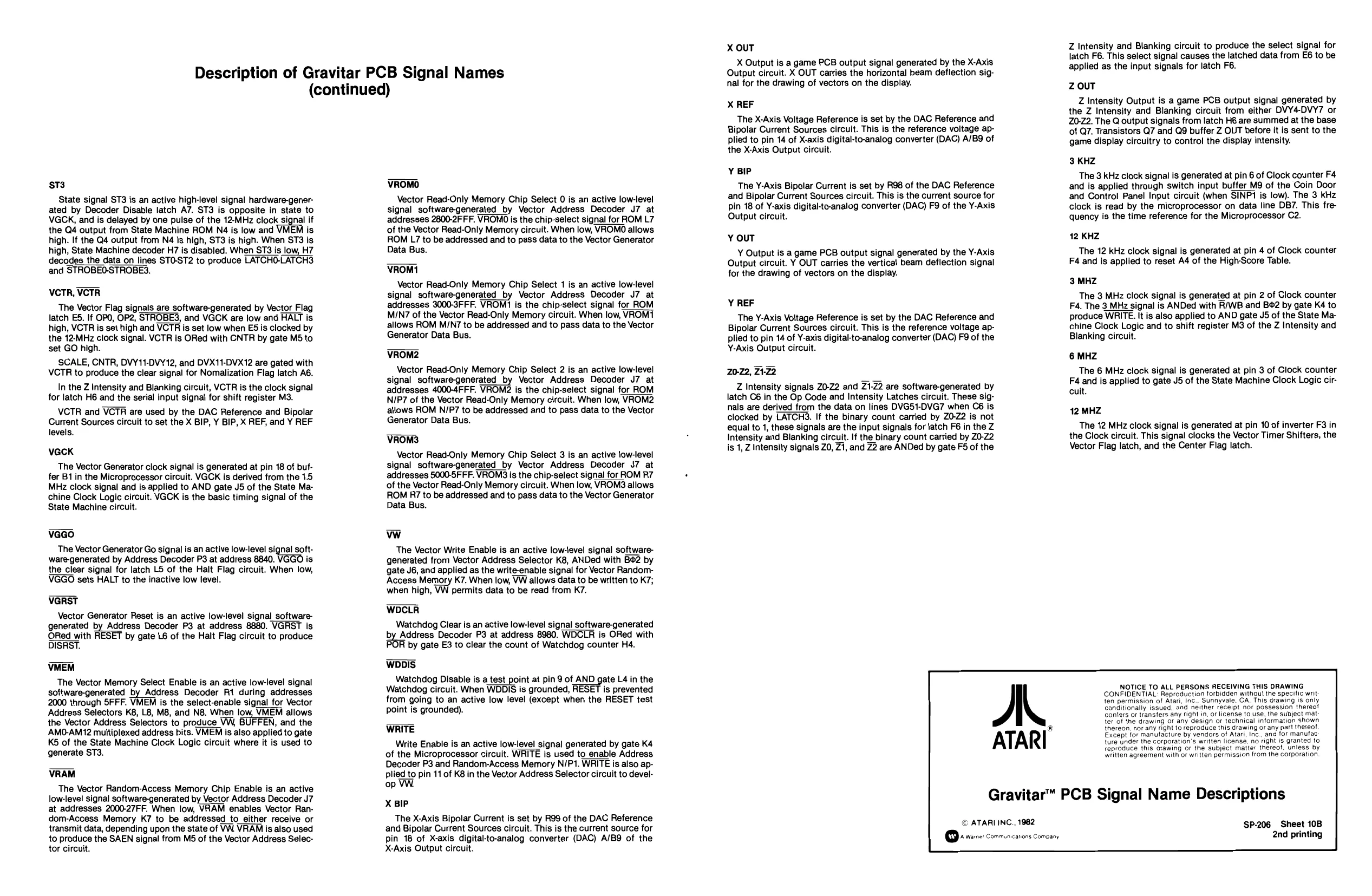
Description of Gravitar PCB Signal Names
(continued)
ST3 State signal ST3 is an active high-level signal hardware-generated by Decoder Disable latch A7. ST3 is opposite in state to VGCK, and is delayed by one pulse of the 12-MHz clock signal if the Q4 output from State Machine ROM N4 is low and VMEM is high. If the Q4 output from N4 is high, ST3 is high. When ST3 is high, State Machine decoder H7 is disabled. When STS is low, H7 decodes the data on lines STO-ST2 to produce LATCHO-LATCH3 and STROBEO-STROBES.
VCTR, VCTR The Vector Flag signals are software-generated by Vector Flag latch ES. If OPO, OP2, STROBES, and VGCK are low and HALT is high, VCTR is set high and VCTR is set low when ES is clocked by the 12-MHz clock signal. VCTR is ORed with CNTR by gate M5 to set GO high. SCALE, CNTR, DVY11-DVY12, and DVX11-DVX12 are gated with VCTR to produce the clear signal for Nomalization Flag latch A6. In the Z Intensity and Blanking circuit, VCTR is the clock signal for latch H6 and the serial input signal for shift register M3. VCTR and VCTR are used by the DAC Reference and Bipolar Current Sources circuit to set the X BIP, Y BIP, X REF, and Y REF levels.
VGCK The Vector Generator clock signal is generated at pin 18 of buffer B1 in the Microprocessor Circuit. VGCK is derived from the 1.5 Mz clock signal and is applied to AND gate J5 of the State Machine Clock Logic circuit. VGCK is the basic timing signal of the State Machine circuit.
VGGO The Vector Generator Go signal is an active low-level signal soft-
ware-generated by Address Decoder P3 at address 9840. VGGO is
the clear signal for latch L5 of the Halt Flag circuit. When low, VGGO sets HALT to the inactive low level.
VGRST Vector Generator Reset is an active low-level signal_softwaregenerated by Address Decoder P3 at address 8880. VGRST is ORed with RESET by gate L6 of the Halt Flag circuit to produce DISRST.
VMEM The Vector Memory Select Enable is an active low-level signal ‘software-generated by Address Decoder R1 during addresses 2000 through SFFF. VMEM is the select-enable signal for Vector Address Selectors K8, L8, M8, and N8. When low, VMEM allows the Vector Address Selectors to produce VW, BUFFEN, and the AMO-AM12 multiplexed address bits. VMEM is also applied to gate K5 of the State Machine Clock Logic circuit where it is used to generate ST3.
VRAM The Vector Random-Access Memory Chip Enable is an active low-level signal software-generated by Vector Address Decoder J7 at addresses 2000-27FF. When low, VRAM enables Vector Random-Access Memory K7 to be addressed to either receive or transmit data, depending upon the state of VW. VRAM is also used to produce the SAEN signal from M5 of the Vector Address Selector circuit. VROMO Vector Read-Only Memory Chip Select 0 is an active low-level signal software-generated by Vector Address Decoder J7 at addresses 2800-2F FF. VROMO is the chip-select signal for ROM L7 of the Vector Read-Only Memory circuit. When low, VROMO allows
ROM L7 to be addressed and to pass data to the Vector Generator
ata Bus.
VROM1 Vector Read-Only Memory Chip Select 1 is an active low-level signal software-generated_by Vector Address Decoder J7 at addresses 3000-3FFF. VROM1 is the chip-select signal for ROM MIN7 of the Vector Read-Only Memory circuit. When low, VROM7 allows ROM MIN7 to be addressed and to pass data to the Vector Generator Data Bus.
VROM2 Vector Read-Only Memory Chip Select 2 is an active low-level signal software-generated by Vector Address Decoder J7 at addresses 4000-4FFF. VROM2 is the chip-select signal for ROM N/P7 of the Vector Read-Only Memory circuit. When low, VROM2 allows ROM N/P7 to be addressed and to pass data to the Vector Generator Data Bus.
VROM3 Vector Read-Only Memory Chip Select 3 is an active low-level signal software-generated by Vector Address Decoder J7 at addresses 5000-5FFF. VROM3 is the chip-select signal for ROM R7 of the Vector Read-Only Memory circuit. When low, VROMS allows ROM 7 to be addressed and to pass data to the Vector Generator Data Bus.
vw The Vector Write Enable is an active low-level signal softwaregenerated from Vector Address Selector K8, ANDed with BO2 by gate J6, and applied as the write-enable signal for Vector Random- Access Memory K7. When low, VW allows data to be written to K7; when high, VW permits data to be read from K7.
WDCLR Watchdog Clear is an active low-level signal software-generated
Ban tress Decoder P3 at address 8980. WDCLR is ORed with
by gate E3 to clear the count of Watchdog counter H4.
WDDIS. Watchdog Disable is a test point at pin 9 of AND gate L4 in the Watchdog circuit. When WDDIS is grounded, RESET is prevented from going to an active low level (except when the RESET test point is grounded).
WRITE Write Enable is an active low-level signal generated by gate K4 of the Microprocessor circuit. WRITE is used to enable Address Decoder P3 and Random-Access Memory N/P1. WRITE is also applied to pin 11 of K8 in the Vector Address Selector circuit to develop WW
X BIP The X-Axis Bipolar Current is set by R99 of the DAC Reference and Bipolar Current Sources circuit. This is the current source for pin 18 of X-axis digital-to-analog converter (DAC) A/B9 of the X-Axis Output circuit. X OUT X Output is a game PCB output signal generated by the X-Axis Output circuit. X OUT carries the horizontal beam deflection signal for the drawing of vectors on the display.
Xx REF The X-Axis Voltage Reference is set by the DAC Reference and Bipolar Current Sources circuit. This is the reference voltage applied to pin 14 of X-axis digital-to-analog converter (DAC) A/B9 of the X-Axis Output circuit.
Y BIP The Y-Axis Bipolar Current is set by R98 of the DAC Reference and Bipolar Current Sources circuit. This is the current source for pin 18 of Y-axis digital-to-analog converter (DAC) F9 of the Y-Axis Output circuit.
Y OUT Y Output is a game PCB output signal generated by the Y-Axis Output circuit. Y OUT carries the vertical beam deflection signal for the drawing of vectors on the display.
Y REF The Y-Axis Voltage Reference is set by the DAC Reference and Bipolar Current Sources circuit. This is the reference voltage applied to pin 14 of Y-axis digital-to-analog converter (DAC) F9 of the Y-Axis Output circuit.
20-22, Z1-22 Z Intensity signals Z0-Z2 and 21-22 are software-generated by latch C6 in the Op Code and Intensity Latches circuit. These signals are derived from the data on lines DVG51-DVG7 when C6 is clocked by LATCH. If the binary count carried by 20-22 is not equal to 1, these signals are the input signals for \atch F6 in the Z Intensity and Blanking circuit. If the binary count carried by Z0-22 is 1, Z Intensity signals ZO, Zi, and Z2 are ANDed by gate F5 of the
A
ATARI
Z Intensity and Blanking circuit to produce the select signal for latch F6. This select signal causes the latched data from E6 to be applied as the input signals for latch F6.
Z OUT Z Intensity Output is a game PCB output signal generated by the Z Intensity and Blanking circuit from either DVY4-DVY7 or 20-22. The Q output signals from latch H6 are summed at the base of Q7. Transistors Q7 and Q9 buffer Z OUT before it is sent to the game display circuitry to control the display intensity.
3 KHZ The 3 kHz clock signal Is generated at pin 6 of Clock counter F4 and is applied through switch input buffer M9 of the Coin Door and Control Panel Input circuit (when SINP1 is low). The 3 kHz clock is read by the microprocessor on data line DB7. This frequency is the time reference for the Microprocessor C2.
12 KHZ The 12 kHz clock signal is generated at pin 4 of Clock counter F4 and is applied to reset A4 of the High-Score Table.
3 MHZ The 3 MHz clock signal is generated at pin 2 of Clock counter F4. The 3 MHz signal is ANDed with R/WB and B@2 by gate K4 to produce WRITE. It is also applied to AND gate JS5 of the State Machine Clock Logic and to shift register M3 of the Z Intensity and Blanking circuit.
6 MHZ The 6 MHz clock signal is generated at pin 3 of Clock counter F4 and is applied to gate J5 of the State Machine Clock Logic circuit.
12 MHZ The 12 MHz clock signal is generated at pin 10 of inverter F3 in the Clock circuit. This signal clocks the Vector Timer Shifters, the Vector Flag latch, and the Center Flag latch.
NOTICE TO ALL PERSONS RECEIVING THIS DRAWING CONFIDENTIAL: Reproduction forbidden without the specitic writ ten permission of Atari, Inc., Sunnyvale, CA, This drawing is only conditionally issued, and neither receipt nor possession thereot conters or transfers any right in, oF license to use. the subject mat. ter of the drawing or any design or technical information shown thereon. nor any right to reproduce this drawing or any part thereo! Except for manufacture by vendors of Atari, Inc., and for manufac: ture under the corporation's written license, no right is granted to reproduce this drawing or the subject matter thereof. unless by written agreement with or written permission from the corporation.
Gravitar™ PCB Signal Name Descriptions
© ATARI INC., 1982 SP-206 Sheet 10B
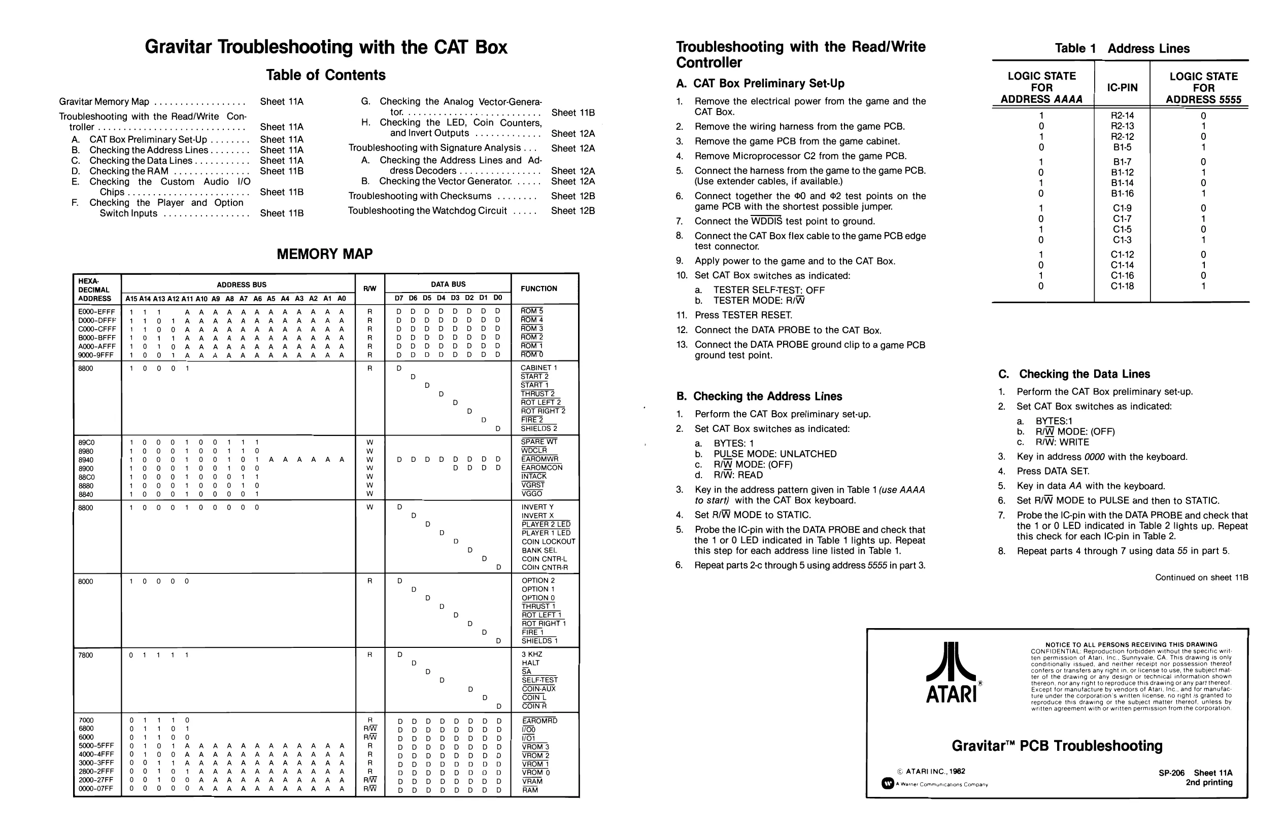
Gravitar Troubleshooting with the CAT Box
Table of Contents
Gravitar Memory Map ..........000eeeee Troubleshooting with the Read/Write Controller... eee eee eee CAT Box Preliminary Set-Up . Checking the Address Lines . Checking the Data Lines . Checking the RAM os Checking the Custom Audio I/O CHIPS cc. cs nieces pene aemewas Checking the Player and Option Switch Inputs .............0.65 nm mooOm>
HEXA- DECIMAL ADDRESS Sheet 114 G. Checking the Analog Vector-Genera- | (0) Sheet 114 H. Checking the LED, Coin Sheet 11 and Invert Outputs Sheet 114 Troubleshooting with Signature Analysis . Sheet 114 A. Checking the Address Lines and Ad: Sheet 11B dress Decoders B. Checking the Vector Generator. Sheet 11B Troubleshooting with Checksums . . Sheet 11B Toubleshooting the Watchdog Circuit .....
MEMORY MAP
DATA BUS ADDRESS | A15 A14 A13 A12 A11 A10 AQ AB D3 Sheet 11B
Sheet 12A
Sheet 12A
Sheet 12A Sheet 12A Sheet 12B Sheet 12B
E000-EFFF (D000-DFFF C000-CFFF B000-BFFF ‘A000-AFFF 9000-9F FF +404 popeo>(B
8800
S/SSseeee
PLAYER 1 LED COIN LOCKOUT BANK SEL COIN CNTR-L COIN CNTR-R
7000 6800 6000 5000-5FFF 4000-4F FF 3000-3FFF 2800-2FFF 2000-27FF 0000-07FF AM Troubleshooting with the Read/Write Controller
A. CAT Box Preliminary Set-Up
- Remove the electrical power from the game and the CAT Box. Remove the wiring harness from the game PCB. Remove the game PCB from the game cabinet. Remove Microprocessor C2 from the game PCB. Connect the harness from the game to the game PCB. (Use extender cables, if available.)
- Connect together the 0 and ©2 test points on the game PCB with the shortest possible jumper.
- Connect the WDDIS test point to ground.
Connect the CAT Box flex cable to the game PCB edge test connector.
- Apply power to the game and to the CAT Box.
- Set CAT Box switches as indicated: a. TESTER SELF-TEST: OFF b. TESTER MODE: R/W
- Press TESTER RESET.
- Connect the DATA PROBE to the CAT Box.
- Connect the DATA PROBE ground clip to a game PCB ground test point. FY PFOnN
B. Checking the Address Lines
- Perform the CAT Box preliminary set-up.
- Set CAT Box switches as indicated: a. BYTES: 1 b. PULSE MODE: UNLATCHED c. R/W MODE: (OFF) d. R/W: READ
- Key in the address pattern given in Table 1 (use AAAA to start} with the CAT Box keyboard.
- Set RIW MODE to STATIC.
- Probe the IC-pin with the DATA PROBE and check that the 1 or 0 LED indicated in Table 1 lights up. Repeat this step for each address line listed in Table 1.
- Repeat parts 2-c through 5 using address 5555 in part 3.
A, ATARI Table 1 Address Lines
LOGIC STATE LOGIC STATE FOR IC-PIN FOR ADDRESS AAAA ADDRESS 5555
1 R2-14 0 0 R2-13 1 1 R2-12 0 0 BIS 1
1 B17 0 0 B1-12 1 1 B1-14 0 0 B1-16 1
1 c19 0 0 C17 1 1 C15 0 0 C13 1 1 C112 0 0 C1-14 1 1 C116 0 0 01-18 1
C. Checking the Data Lines 1.
2.
NOAPR ow Perform the CAT Box preliminary set-up. Set CAT Box switches as indicated: a BYTES: b. R/W MODE: (OFF) c. R/W: WRITE Key in address 0000 with the keyboard. Press DATA SET.
Key in data AA with the keyboard. Set R/W MODE to PULSE and then to STATIC. Probe the IC-pin with the DATA PROBE and check that the 1 or 0 LED indicated in Table 2 lights up. Repeat this check for each IC-pin in Table 2. Repeat parts 4 through 7 using data 56 in part 5.
Continued on sheet 11B
NOTICE TO ALL PERSONS RECEIVING THIS DRAWING CONFIDENTIAL: Reproduction forbidden without the specific writ: ten permission of Atari, Inc., Sunnyvale, CA. This drawing is only conditionally issued, and neither receipt nor possession thereot confers or transfers any right in. or license to use, the subject mat ter of the drawing or any design or technical information shown thereon. nor any right to reproduce this drawing or any par! thereot Except for manufacture by vendors of Atari, Inc.. and for manutac ture under the corporation's written license. no right 's granted to reproduce this drawing or the subject matter thereof, unless by written agreement with or written permission from the corporation
Gravitar™ PCB Troubleshooting
© ATARI INC., 1982 SP-206 Sheet 11A
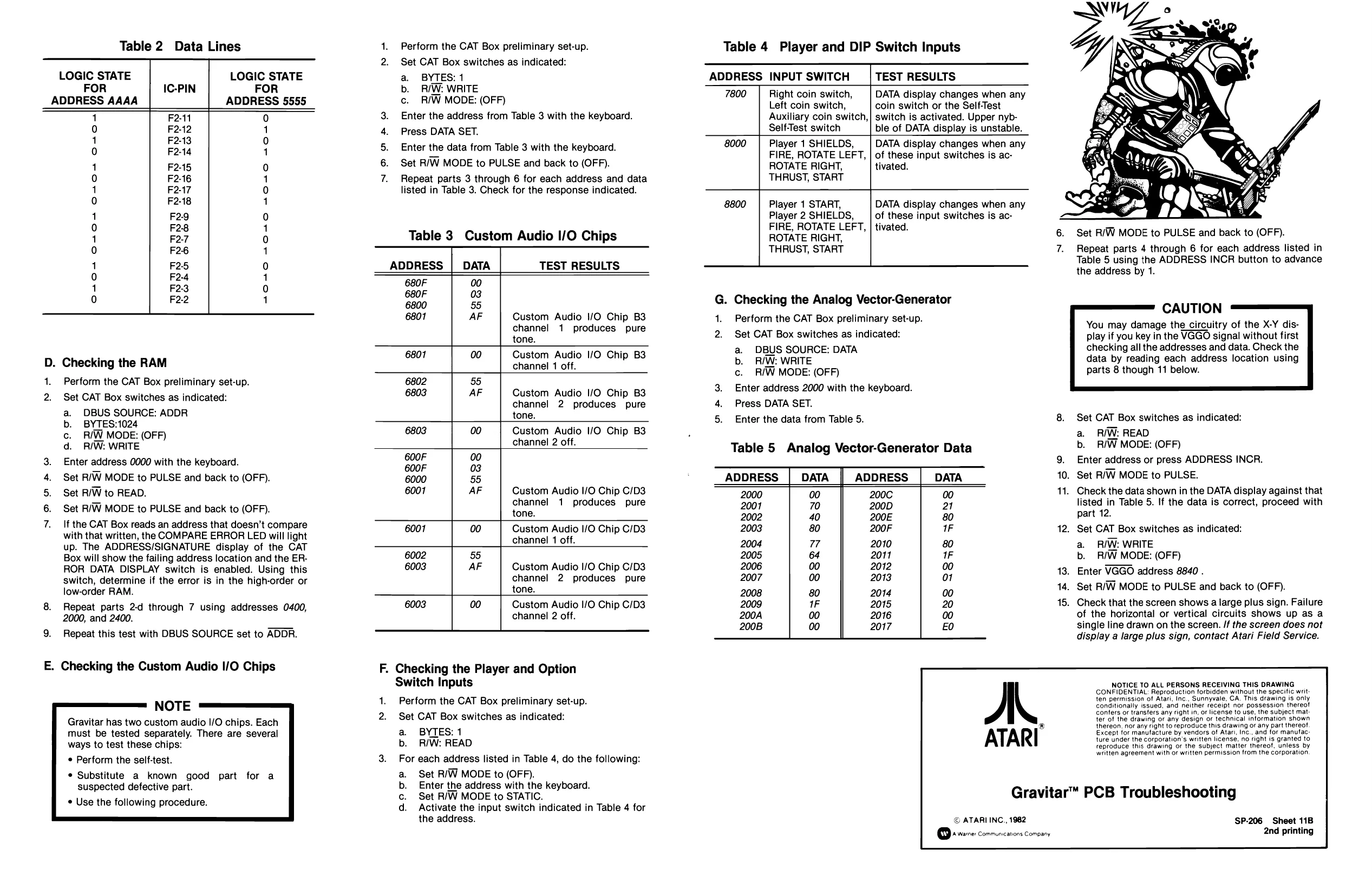
| Table 2 | Data Lines | 1. | Perform the CAT Box preliminary set-up. | Table 4 | Player and DIP Switch Inputs |
- Set CAT Box switches as indicated:
| LORIC STATE | 7 | LOGIC STATE | a. | BYTES: 1 | ADDRESS INPUT SWITCH | TEST RESULTS | |
| IC-PIN | FOR | b. | R/W: WRITE | " | > | ri | 7 |
| pas | . | 7800 | Right coin switch, | DATA display changes when any | |||
| ADDRESS AAAA | ADDRESS 5555 | c. | R/W MODE: (OFF) | ; | Left coin switch, | coin switch or the Self-Test | |
| 1 | F2-11 | 0 | 3. | Enter the address from Table 3 with the keyboard. | Auxiliary coin switch,| switch is activated. Upper nyb- | ||
| 0 | F212 | 1 | 4. | Press DATA SET. | Self-Test switch | ble of DATA display is unstable. | |
| 0 | at | ; | 5. | Enter the data from Table 3 with the keyboard. | 8000 | ree OTE PEET, | oa display changes when any |
| : | F245 | P | 6. | Set R/W MODE to PULSE and back to (OFF). | ROTATERIGHT | '|tvated |
fe) F216 1 7. Repeat parts 3 through 6 for each address and data THRUST, START
| 1 | F217 | 0 | listed in Table 3. Check for the response indicated. | ||||
| 0 | F218 | 1 | 8800 | Player 1 START, | DATA display changes when any | ||
| 1 | F2.9 | 0 | Player 2 SHIELDS, | of these input switches is ac- | |||
| 0 | F2-8 | 1 | . | . | FIRE, ROTATE LEFT, | tivated. | ||
| 1 | F2.7 | 0 | Table 3 | Custom Audio I/O Chips | ROTATE RIGHT, | 6. | Set R/W MODE to PULSE and back to (OFF). |
| 0 | F2-6 | 1 | THRUST, START | 7. | Repeat parts 4 through 6 for each address listed in |
1 . a Table 5 using the ADDRESS INCR button to advance
| } | faa | ° | ADDRESS | DATA | TEST RESULTS | the address by 1. |
| 1 | F2-3 | 0 | 680F | 00 | |
| : | a | a | hecking | the Analog | Vector-G |
0 F22 1 6800 55 G. Checking the Analog Vector-Generator CAUTION
| 6801 | AF | Custom Audio 1/0 Chip B3 | 4. | Perform the CAT Box preliminary set-up. | a | . | ||||||
| channel | 1 | produces pure | q | indi | . | You may damage the circuitry of the X-Y dis- | ||||||
| tone. | 2. | Set CAT Box switches as indicated: | play if you key in the VGGO signal without first | |||||||||
| ji | A | a. | DBUS SOURCE: DATA | checking all the addresses and data. Check the | ||||||||
| D. Checking the RAM | ad | 7 | Seal ot Wore es | b. | R/W: WRITE | data by reading each address location using | ||||||
| 1. | Perf | the CAT Bo: | fl | 6802 | 5 | cemete | c. | IW MODE: (OFF) | parts 8 though 11 below. | |||
| . | erform | the | x preliminary set-up. | 5 | j | |||||||
| 2. | Set CAT Box switches as indicated: | 6803 | AF | Custom Audio I/O Chip B3 | it | Enter adores 2000 with the keyboard. | ||||||
| a. | DBUS SOURCE: ADDR | channel 2 produces pure | 4. | Press DATA SET. | ||||||||
| b. | BYTES:1024 | tone. | Enter the data from Table 5. | 8. | Set CAT Box switches as indicated: | |||||||
| c. | R/W MODE: (OFF) | 6803 | 00 | Custom Audio I/O Chip B3 | a. | R/W: READ | ||||||
| d. | RIW: WRITE | channel 2 off. | Table 5 | Analog Vector-Generator Data | b. | RIW MODE: (OFF) | ||||||
| 3. | Enter address 0000 with the keyboard. | a | 0 | 9. | Enter address or press ADDRESS INCR. | |||||||
| 4. | Set R/W MODE to PULSE and back to (OFF). | 6000 | 55 | ADDRESS. | DATA | ADDRESS | DATA | 10. Set R/W MODE to PULSE. | ||||
| 5. | Set RIW to READ. | 6001 | AF | Custom Audio I/O Chip C/D3 | 2000 | 00 | 2000 | 00 | 11. Check the data shown in the DATA display against that | |||
| 6. | Set RIW MODE to PULSE and back to (OFF. | channel | 1 | produces pure | 2001 | 70 | 200D | 21 | listed in Table 5. If the data is correct, proceed with | |||
| 7. | If the CAT Box reads an address that doesn’t compare | tore: | a | ao | 200F | be | parte: | |||||
| with that written, the COMPARE ERROR LED will light | 6001 | 00 | Custom ate 1/0 Chip C/D3 | 2003 | 80 | 200F | 1F | 12. Set CAT Box switches as indicated: | ||||
| up. The ADDRESS/SIGNATURE display of the CAT | . | 2004 | 7 | 2010 | 80 | a. | R/W: WRITE | |||||
| Box will show the failing address location and the ER- | ene | 2 | Custom | Audio | vO Chia | ¢ | ore | 64 | 2017 | 1F | b. | R/W MODE: (OFF) |
| ROR DATA DISPLAY switch is enabled. Using this | ‘ustom Audio | | | hip C/D3 | 00 | 2072 | 00 | VGGO | addi | ||||
| switch, determine if the error is in the high-order or | channel 2 produces pure | 2007 | 00 | 2013 | on | 1S, Enter WGGO andres 840: | ||||||
| low-order RAM. | tone. | 2008 | 80 | 2014 | 00 | 14. Set R/W MODE to PULSE and back to (OFF). | ||||||
| 8. | Repeat parts 2-d through 7 using addresses 0400, | 6003 | 00 | Custom Audio I/O Chip C/D3 | 2009 | 1F | 2015 | 20 | 15. Check that the screen shows a large plus sign. Failure | |||
| 2000, and 2400. | channel 2 off. | 200A | 00 | 2016 | 00 | of the horizontal or vertical circuits shows up as a | ||||||
| , | ‘ | =— | 200B | 00 | 2017 | £0 | single line drawn on the screen. /f the screen does not | |||||
| 9. | Repeat this test with DBUS SOURCE set to ADDR. | display a large plus sign, contact Atari Field Service. |
E. Checking the Custom Audio I/O Chips F. Checking the Player and Option
Switch Inputs
Perform the CAT Box preliminary set-up. A NOTICE TO ALL PERSONS RECEIVING THIS DRAWING CONFIDENTIAL: Reproduction forbidden without the specific writ ten permission of Atari, Inc., Sunnyvale, CA. This drawing is only conditionally issued, and neither receipt nor possession thereof
confers or transfers any right in, or license to use. the subject mat
| Gravitar has two custom audio I/O chips. Each | 2) | Set GAT BoxiswitchesiasIndicated: | fer of the drawing or any design or technical iniormation shown | |
| must be tested separately. There are several | a | BYTES: 1 | te | Eecepr ior menuteeture by vendors of Ata Ine. and for manufac |
| waye Ip tee tess enips: | By | BNEIREAD | ATARI | ae rere ine subject malice Maret, antes Oy |
| * Perform the self-test. | 3. | For each address listed in Table 4, do the following: | wtten agreement with or written permission from the corporation |
¢ Substitute a known good part for a suspected defective part. Use the following procedure. a. Set R/W MODE to (OFF). b. Enter the address with the keyboard. c. Set R/W MODE to STATIC. d. Activate the input switch indicated in Table 4 for the address. Gravitar™ PCB Troubleshooting © ATARIINC., 1982 SP-206 Sheet 11B
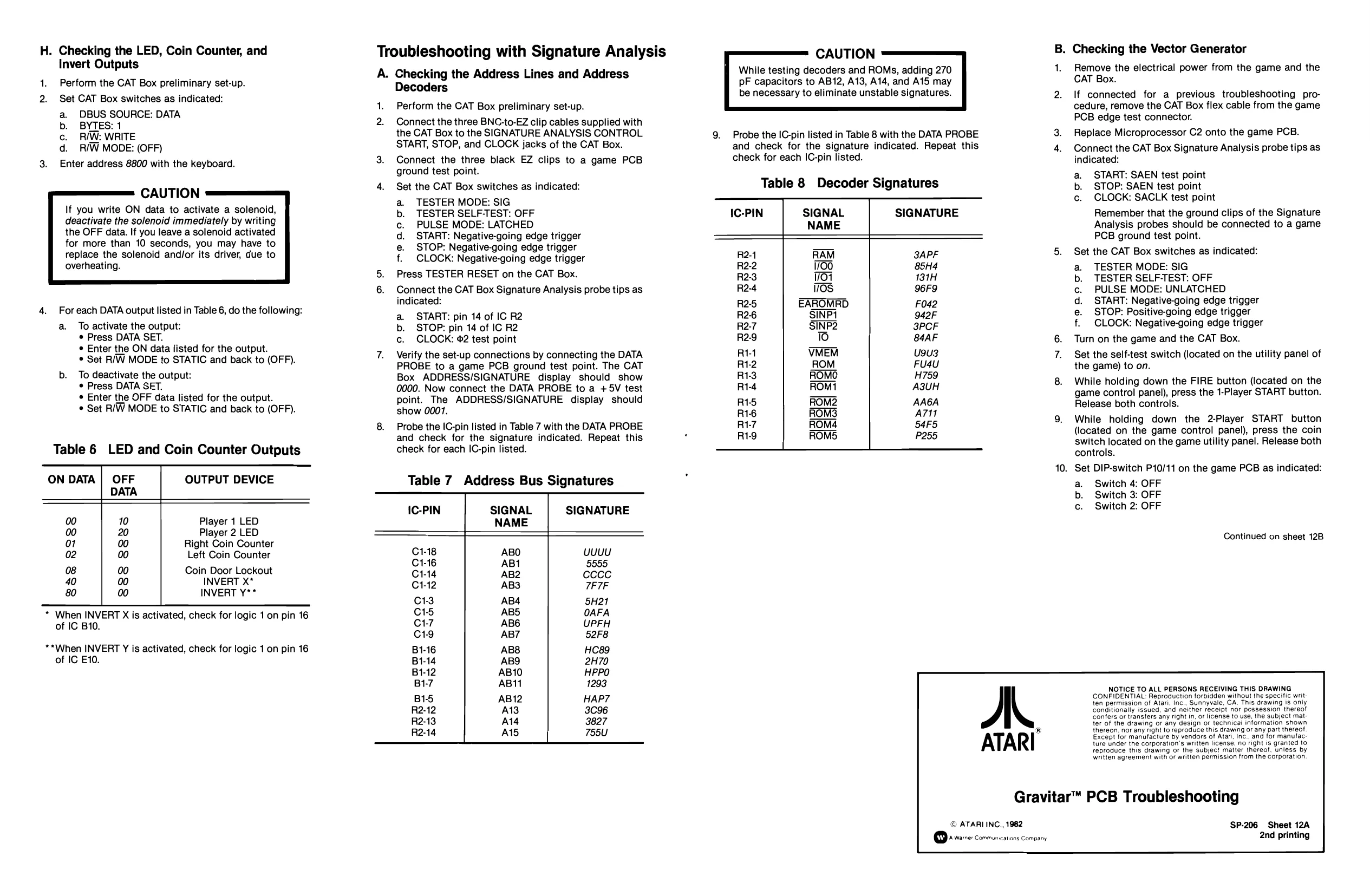
H. Checking the LED, Coin Counter, and
Invert Outputs
Perform the CAT Box preliminary set-up. Set CAT Box switches as indicated: a. DBUS SOURCE: DATA b. BYTES: 1 c. RIW: WRITE d. IW MODE: (OFF) Enter address 8800 with the keyboard.
For each DATA output listed in Table 6, do the following: a. To activate the output: ¢ Press DATA SET.
- Enter the ON data listed for the output.
- Set R/W MODE to STATIC and back to (OFF). b. To deactivate the output: Press DATA SET.
- Enter the OFF data listed for the output.
- Set R/W MODE to STATIC and back to (OFF).
Table 6 LED and Coin Counter Outputs
ON DATA | OFF OUTPUT DEVICE DATA
| 00 | 10 | Player 1 LED |
| 00 | 20 | Player 2 LED |
01 00 Right Coin Counter
02 00 Left Coin Counter 08 00 Coin Door Lockout
| 40 | 00 | INVERT X* |
| 80 | 00 | INVERT Y** |
- When INVERT X is activated, check for logic 1 on pin 16 of IC B10.
**When INVERT Y is activated, check for logic 1 on pin 16 of IC E10.
Troubleshooting with Signature Analysis
A. Checking the Address Lines and Address Decoders
- Perform the CAT Box preliminary set-up.
- Connect the three BNC-to-EZ clip cables supplied with the CAT Box to the SIGNATURE ANALYSIS CONTROL, START, STOP, and CLOCK jacks of the CAT Box.
- Connect the three black EZ clips to a game PCB ground test point.
- Set the CAT Box switches as indicated: a. TESTER MODE: SIG b. TESTER SELF-TEST: OFF c. PULSE MODE: LATCHED d. START: Negative-going edge trigger e. STOP: Negative-going edge trigger f. CLOCK: Negative-going edge trigger
- Press TESTER RESET on the CAT Box.
- Connect the CAT Box Signature Analysis probe tips as indicated: a. START: pin 14 of IC R2 b. STOP: pin 14 of IC R2 c. CLOCK: 42 test point
- Verify the set-up connections by connecting the DATA PROBE to a game PCB ground test point. The CAT Box ADDRESS/SIGNATURE display should show 0000. Now connect the DATA PROBE to a +5V test point. The ADDRESS/SIGNATURE display should show 0001.
- Probe the IC-pin listed in Table 7 with the DATA PROBE and check for the signature indicated. Repeat this check for each IC-pin listed.
Table 7 Address Bus Signatures
IC-PIN SIGNAL SIGNATURE NAME
C1-18 ABO UUUU
| C1-16 | ABI | 5555 |
| 1-14 | AB2 | CcCcc |
| C1-12 | AB3 | 7F7F |
| C1-3 | AB4 | 5H21 |
| C15 | ABS | OAFA |
| C1-7 | AB6 | UPFH |
| C19 | AB7 | 52F8 |
| B1-16 | ABB | HC89 |
| B1-14 | ABO | 2H70 |
| B1-12 | AB10 | HPPO |
| B17 | ABI1 | 1293 |
| B15 | AB12 | HAP7 |
| R2-12 | A13 | 3C96 |
| R2-13 | A14 | 3827 |
| R2-14 | AIS | 755U |
Probe the IC-pin listed in Table 8 with the DATA PROBE and check for the signature indicated. Repeat this check for each IC-pin listed.
Table 8 Decoder Signatures
IC-PIN SIGNAL SIGNATURE NAME
R21 RAM SAPF
| R22 | 1700 | 85H4 |
| R23 | 101 | 131H |
| R2-4 | i708 | 96F9 |
| R25 | EAROMRD | F042 |
| R26 | SINP1 | 942F |
| R27 | SINP2 | 3PCF |
| R29 | T | 84AF |
| RV | VMEM | usu3 |
| R12 | ‘ROM. | FU4U |
| R13 | ROMO | H759 |
| Rt-4 | ROM1 | A3UH |
| R15 | ROM2 | AAGA |
| R16 | ROM3 | A711 |
| R17 | ROM4 | 54F5 |
| R19 | ROM5 | P255 |
A ATARI . Checking the Vector Generator Remove the electrical power from the game and the CAT Box. If connected for a previous troubleshooting procedure, remove the CAT Box flex cable from the game PCB edge test connector. Replace Microprocessor C2 onto the game PCB. Connect the CAT Box Signature Analysis probe tips as indicated: a. START: SAEN test point b. STOP: SAEN test point c. CLOCK: SACLK test point Remember that the ground clips of the Signature Analysis probes should be connected to a game PCB ground test point. Set the CAT Box switches as indicated: TESTER MODE: SIG TESTER SELF-TEST: OFF PULSE MODE: UNLATCHED START: Negative-going edge trigger STOP: Positive-going edge trigger CLOCK: Negative-going edge trigger Turn on the game and the CAT Box. Set the self-test switch (located on the utility panel of the game) to on. While holding down the FIRE button (located on the game control panel), press the 1-Player START button. Release both controls. While holding down the 2-Player START button (located on the game control panel), press the coin switch located on the game utility panel. Release both controls. roaeop
. Set DIP-switch P10/11 on the game PCB as indicated: a. Switch 4: OFF b. Switch 3: OFF c. Switch 2: OFF
Continued on sheet 12B
NOTICE TO ALL PERSONS RECEIVING THIS DRAWING CONFIDENTIAL: Reproduction forbidden without the specific writ ten permission of Atari, Inc., Sunnyvale, CA. This drawing is only conditionally issued, and neither receipt nor possession thereot confers or transters any right in, oF license to use, the subject mat: ter of the drawing or any design or technical information shown
thereon. nor any right to reproduce this drawing or any part thereot
Except for manufacture by vendors of Atari, Inc., and for manufac ture under the corporation's written license, no right is granted to reproduce this drawing or the subject matter thereof. unless by written agreement with or written permission from the corporation
Gravitar™ PCB Troubleshooting
© ATARI INC., 1962 salons Company SP-206 Sheet 12A
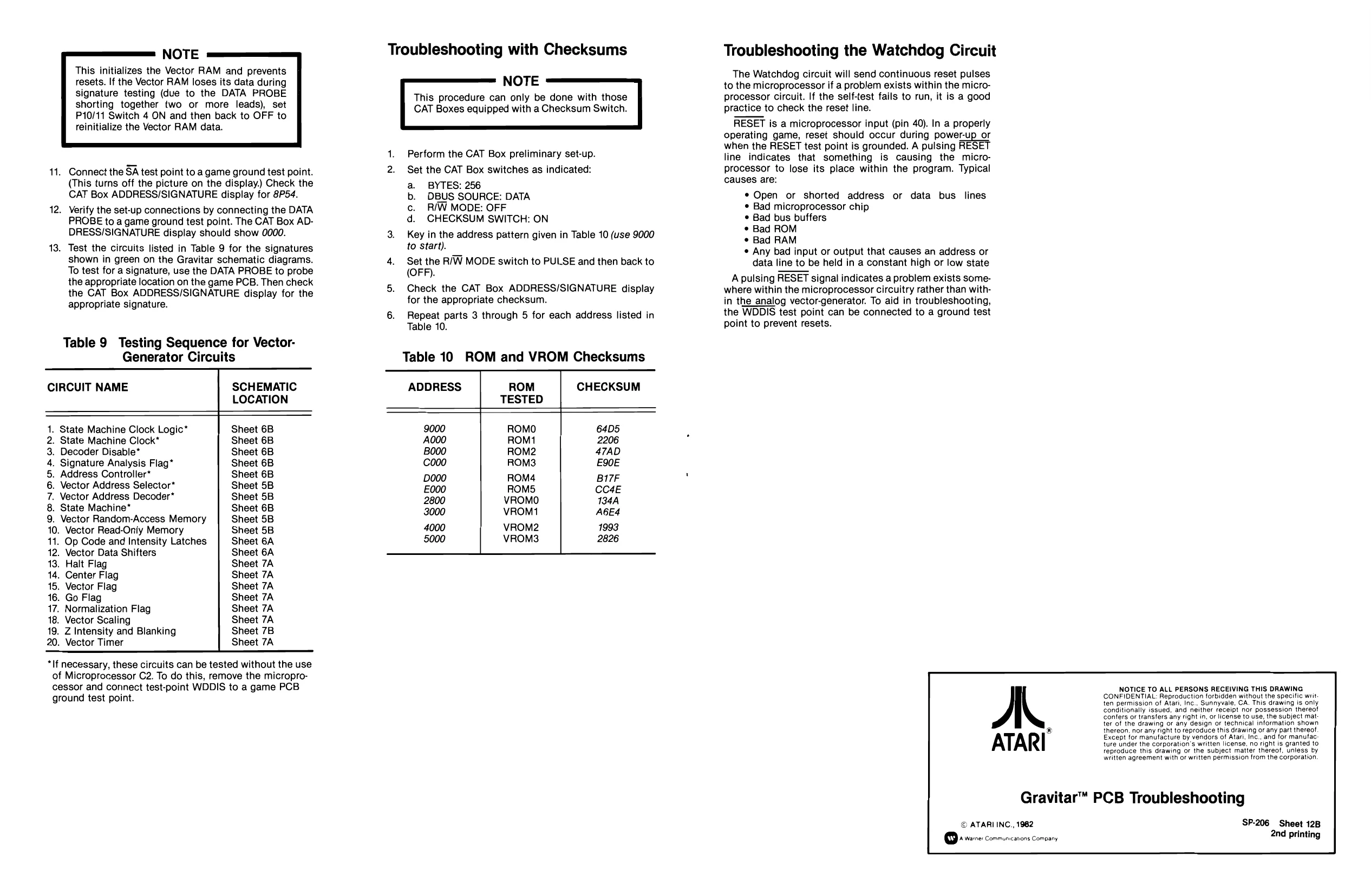
- Connect the SA test point to a game ground test point. (This turns off the picture on the display.) Check the CAT Box ADDRESS/SIGNATURE display for 8P54.
- Verify the set-up connections by connecting the DATA PROBE to a game ground test point. The CAT Box AD- DRESS/SIGNATURE display should show 0000.
- Test the circuits listed in Table 9 for the signatures shown in green on the Gravitar schematic diagrams. To test for a signature, use the DATA PROBE to probe the appropriate location on the game PCB. Then check the CAT Box ADDRESS/SIGNATURE display for the appropriate signature.
Table 9 Testing Sequence for Vector- Generator Circuits
CIRCUIT NAME SCHEMATIC LOCATION
- State Machine Clock Logic* Sheet 6B
- State Machine Clock* Sheet 6B
- Decoder Disable* Sheet 6B
- Signature Analysis Flag* Sheet 6B
- Address Controller* Sheet 6B
- Vector Address Selector* Sheet 5B
- Vector Address Decoder* Sheet 5B
- State Machine* Sheet 6B
- Vector Random-Access Memory Sheet 5B
- Vector Read-Oniy Memory Sheet 5B
- Op Code and Intensity Latches Sheet 6A
- Vector Data Shifters Sheet 6A
- Halt Flag Sheet 7A
- Center Flag Sheet 7A
- Vector Flag Sheet 7A
- Go Flag Sheet 7A
- Normalization Flag Sheet 7A
- Vector Scaling Sheet 7A
- Z Intensity and Blanking Sheet 7B
- Vector Timer Sheet 7A
*If necessary, these circuits can be tested without the use of Microprocessor C2. To do this, remove the microprocessor and connect test-point WDDIS to a game PCB ground test point.
Troubleshooting with Checksums
- Perform the CAT Box preliminary set-up.
- Set the CAT Box switches as indicated: a. BYTES: 256 b. DBUS SOURCE: DATA c. R/W MODE: OFF d. CHECKSUM SWITCH: ON
- Key in the address pattern given in Table 10 (use 9000 to start).
- Set the R/W MODE switch to PULSE and then back to (OFF).
- Check the CAT Box ADDRESS/SIGNATURE display for the appropriate checksum.
- Repeat parts 3 through 5 for each address listed in Table 10.
Table 10 ROM and VROM Checksums
ADDRESS ROM CHECKSUM TESTED
| 9000 | ROMO | 64D5 |
| A000 | ROM1 | 2206 |
| B000 | ROM2 | 47AD |
| co00 | ROM3 | E90E |
| D000 | ROM4 | BI7F |
E000 ROMS CC4E
| 2800 | VROMO | 134A |
| 3000 | VROM1 | AGE4 |
| 4000 | VROM2 | 1993 |
| 5000 | VROM3 | 2826 |
Troubleshooting the Watchdog Circuit
The Watchdog circuit will send continuous reset pulses to the microprocessor if a problem exists within the microprocessor circuit. If the self-test fails to run, it is a good practice to check the reset line. RESET is a microprocessor input (pin 40). In a properly operating game, reset should occur during power-up or when the RESET test point is grounded. A pulsing RESET line indicates that something is causing the microprocessor to lose its place within the program. Typical causes are:
- Open or shorted address or data bus lines
- Bad microprocessor chip
- Bad bus buffers
- Bad ROM
- Bad RAM « Any bad input or output that causes an address or data line to be held in a constant high or low state A pulsing RESET signal indicates a problem exists somewhere within the microprocessor circuitry rather than within the_analog vector-generator. To aid in troubleshooting, the WDDIS test point can be connected to a ground test point to prevent resets.
NOTICE TO ALL PERSONS RECEIVING THIS DRAWING CONFIDENTIAL: Reproduction forbidden without the specific writ ten permission of Atari, Inc., Sunnyvale, CA. This drawing is only conditionally issued, and neither receipt nor possession thereo! confers or transfers any right in, or license to use, the subject matter of the drawing or any design or technical information shown ® thereon, nor any right to reproduce this drawing or any part thereof. Except for manufacture by vendors of Atari, Inc., and for manufac: ture under the corporation's written license, no right is granted to reproduce this drawing or the subject matter thereof, unless by written agreement with or written permission from the corporation,
Gravitar™ PCB Troubleshooting
SP-206 Sheet 128 © ATARI INC., 1982
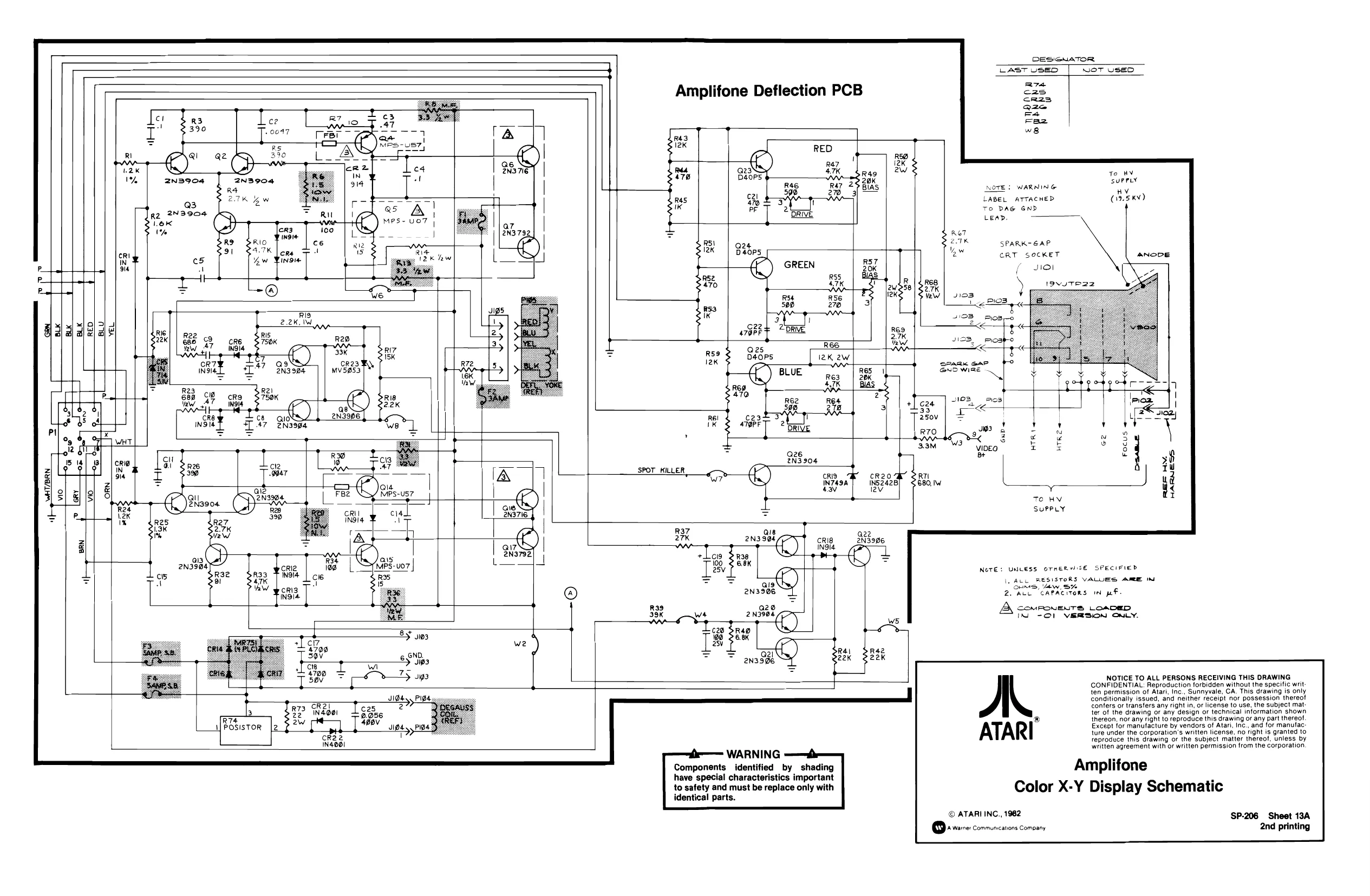
DESeNATOR LAST USED NOT USED
Re c2s cR23 Qz2e ma Faz ws
Amplifone Deflection PCB
To HV
MPS- UOT | SurrLY ‘ NOTE! WARNING NY a3 Mie |. ¢- + LABEL ATTACHED (i. 5 KY) gg 2NB904 To DAG GND LOK Leap.
'* aon ae SPARK- GAP ree rs 12k hw 2M CRT SOCKET JIO1
a
rocus «| Le
SPOT KILLER <—
a22 2N3996
UNLESS OTRERHSE SPECIFIED [ACG RESISTORS VALUES AMEE IN Suns, aw. or
- RUL CAPACITORS Int pF. NeTE:
Ay COMPONENTS LoaDED IND -Ol VERSION ONLY.
O21 2N3906
NOTICE TO ALL PERSONS RECEIVING THIS DRAWING
CONFIDENTIAL: Reproduction forbidden without the specific writ: conters or transfers any right in, or license to use, the subject mat:
ten permission of Atari, Inc., Sunnyvale, CA. This drawing is only conditionally issued, and neither receipt nor possession thereof
ter of the drawing or any design or technical information shown @ thereon, nor any right to reproduce this drawing or any part thereof. Except for manufacture by vendors of Atari, Inc., and for manufac. ture under the corporation's written license, no right is granted to reproduce this drawing or the subject matter thereof, unless by written agreement with or written permission from the corporation.
Amplifone
Color X-Y Display Schematic
IN4OI
© ATARI INC., 1982 ‘SP-206 Sheet 13A
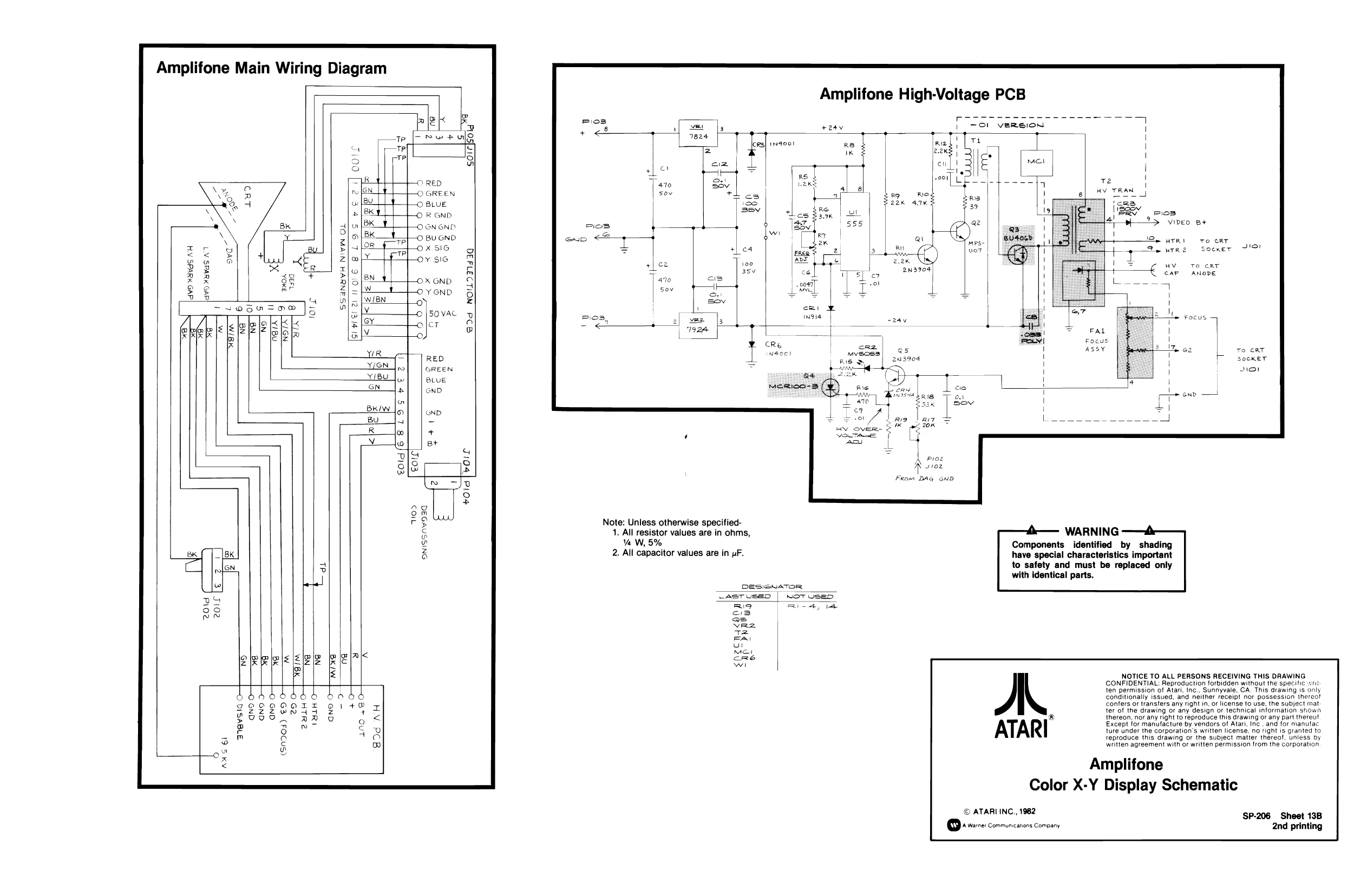
Amplifone Main Wiring Diagram
Amplifone High-Voltage PCB
inaoo!
q
\ +} —2> viveo at i t Nv ‘9 Bay i 3 ' ' ro crt euTR2 Socxer TIO!
HV To cRT CAP ANODE 2N3904 toe dv ¥YWdS NH dv WavaS AT SSANSVH NIVW OL
Si vi ei ei 2d NOIINIIG
as et ro ert 2n3904 s0cKeT 7S sot ( vj enw COld(ES LIT FEZ! corr 41g ¢ @ B'S S588
+0ld[voir I
- All resistor values are in ohms, Ys W, 5%
- All capacitor values are in uF.
DEsioNaTOR Casruses | NoTUSED Rig Bio a3 Ss eed x2 al ci Mey
wi _ te
War
2ULHC 14H confers or transters any right in, or license to use, the subject mat NOTICE TO ALL PERSONS RECEIVING THIS DRAWING
CONFIDENTIAL: Reproduction forbidden without the specific 11
ten permission of Atari, Inc., Sunnyvale, CA, This drawing is only conditionally issued, and neither receipt nor possession thereot
® ter of the drawing or any design or technical information shown aNd 0 ano No «Sn304) €9 4 thereon, nor any right to reproduce this drawing or any part thereof Except for manufacture by vendors of Atari, Inc, and for manufac ture under the corporation's written license, no right is granted to reproduce this drawing or the subject matter thereof, unless by written agreement with or written permission from the corporation. Hevsid 0 1N0 +96
Amplifone
Color X-Y Display Schematic
© ATARI INC., 1982 SP-206 Sheet 13B tere: Communeaions Company 2nd printing
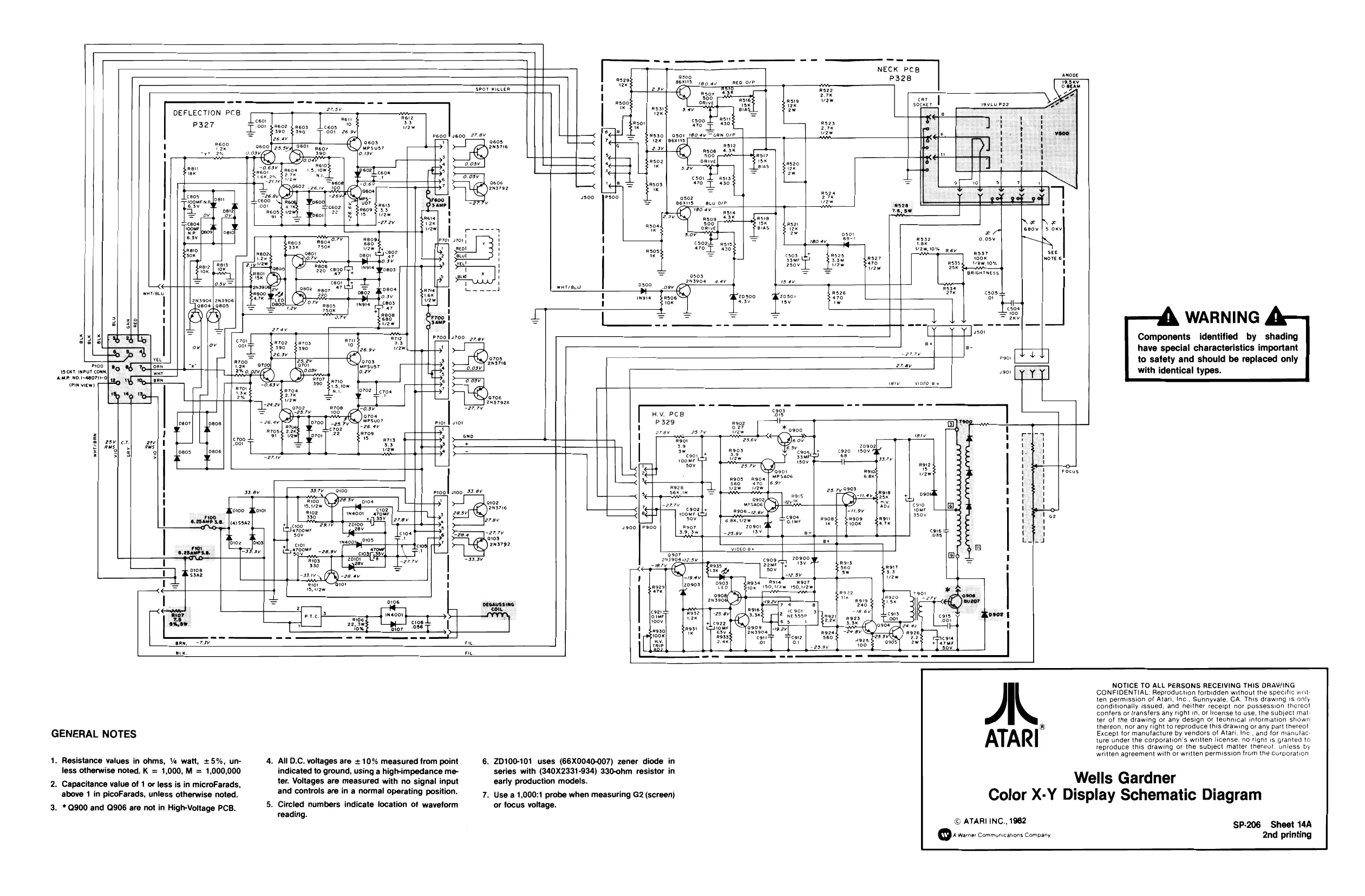
NECK PCB nsze; P328 eee TIE
| worm | ] | wee | —t+ |
-- ! 303 R519 ae Pee | revive » DEFLECTION PCB | P327 6004 s600_27.8v B eS
| mae | (O| | er | + | = | fT |
| <= | eens | au ove | asze | ' |
she
aaa RIG T NESS '
a3 he Components identified by shading oe have special characteristics important
| =e | oc | ihe | an | poor | [YY | to safety and should be replaced only |
| Soiutat cone Be ete | ru | Ups | |e | wo fP YY | with identical types. | |
| ‘omview! | se | | | 7087 | lev | oro es |
ace | LS
| sivew | -_ | ana7i6 |
Roe rwaoor SOR za.sy
| 22 | +38 | brev |
230825 csoad
NOTICE TO ALL PERSONS RECEIVING THIS DRAWING CONFIDENTIAL: Reproduction forbidden without the specific it ten permission of Atari, Inc., Sunnyvale, CA. This drawing is only conditionally issued, and neither receipt nor possession thereo!
confers or ransfers any right in, or license to use, the subject mat
ter of the drawing or any design or technical intormation shown GENERAL NOTES Except ior manufacture by vendors of Atart Ine. and for manulac
Teproduce this drawing or the subject mater theres? uniess by (ahitgn agreement withor witten permission from the corporation
- Resistance values in ohms, % watt, +5%, un- 4. A.C. voltages are + 10% measured from point 6. ZD100-101 uses (66X0040-007) zener diode in
| less otherwise noted. K = 1,000, M = 1,000,000 | indicated to ground, using | a high-impedance me- | series with (340X2331-934) 330-ohm resistor in | |||
| 2. Capacitance value of 1 oF less is in microFarads, | tor. Voltages aro measured with no signal input | early production models. | Wells Gardner | |||
| above 1 in picoFarads, unless otherwise noted. | and controls are in a normal operating position. | 7. Use a 1,000:1 probe when measuring G2 (screen) | *Y | Di | i | i |
- * 0900 and Q906 are not in High-Voltage PCB. 5. Circled numbers indicate location of waveform or focus voltage. Color X-Y Display Schematic Diagram
reading. © ATARI INC., 1982 SP-206 Sheet 14A Qi vare: Communications Company 2nd printing