Centipede Cocktail DP-188-2nd-02B
Centipede (revision 4) (Atari, 1980) · Drawing Package · 1 pages · original scan
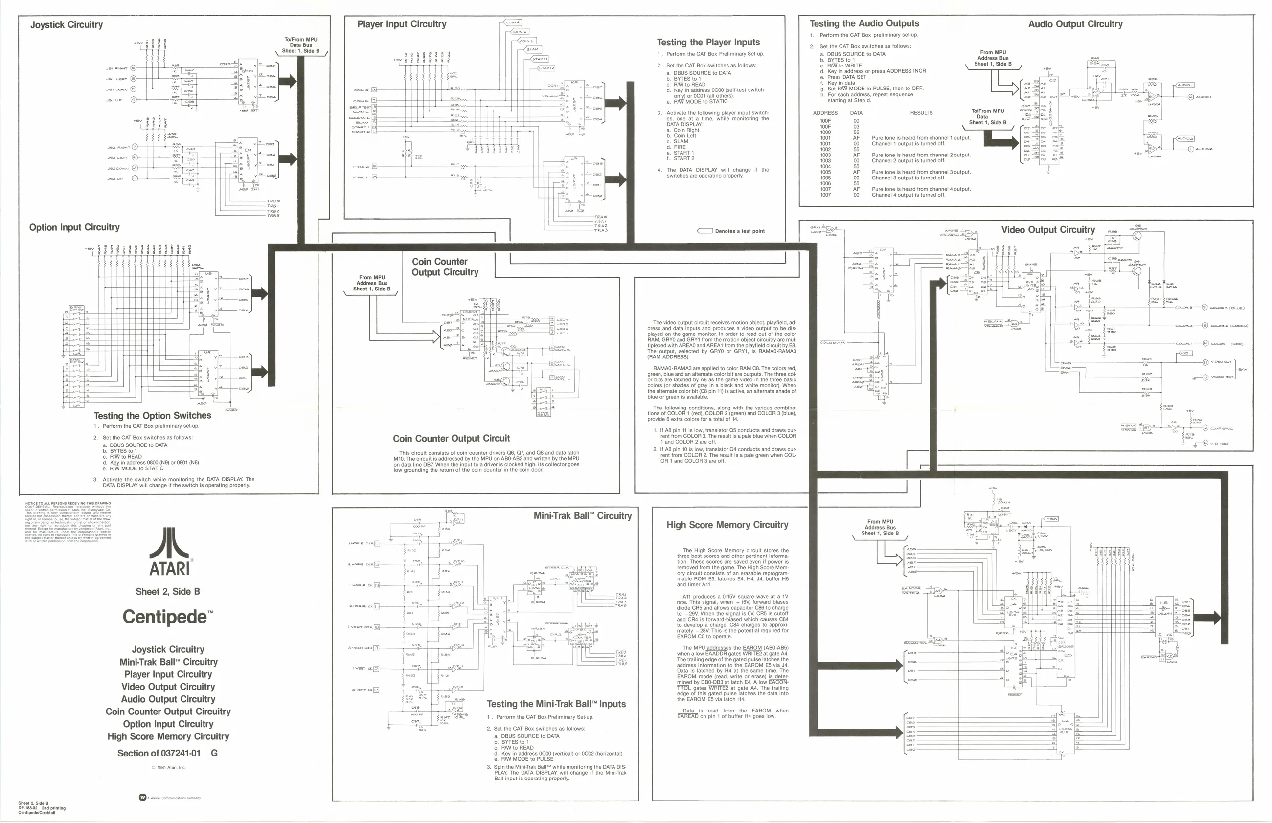
Joystick Circuitry
Testing the Option Switches
Perform the CAT Box preliminary setup.
2. Set the CAT Box switches as follows:
‘BUS SOURCE to DATA BYTES 101 IW to READ Key in address 0800 (NS) or 0801 (NB) FIW MODE to STATIC
- Activate the switch while monitoring the DATA DISPLAY. The DATA DISPLAY will change if the switch is operating properly. TolFrom MPU Data Bus Sheet 1, Side B
Player Input Circuitry
Testing the Player Inputs
41, Perform the GAT Box Preliminary Setup.
‘a. DBUS SOURCE to DATA
b. BYTES to1 ©. RIW to READ
- Key in address 0C00 (selt-test switch ‘only) oF OCO1 (all others). @. FW MODE to STATIC
- Activate the following player input switch: 5, one at a time, while monitoring the DATA DISPLAY:
- Coin Right ». Coin Lett . SLAM
- FIRE fe. START 1 START
- The DATA DISPLAY will change if the ‘switches are operating properly.
Coin Counter Output Circuitry
Coin Counter Output Circuit
This circuit consists of coin counter drivers Q6, Q7, and Q8 and data latch 'M10, The circuit is addressed by the MPU on AB0-AB2 and written by the MPU. ‘on data line DB7. When the input to a diver is clocked high, its collector goes, Tow grounding the retum of the coin counter in the coin door.
L ‘The video output circuit receives motion object, playfield, ad dress and data inputs and produces a video output to be displayed on the game monitor. In order 1 read oul of the color RAM, GRYO ang GRY1 from the motion object circuitry are mut tiplexed with AREAO and AREA trom the playfield ciroult by EB. The output, selected by GRYO or GRY1, is RAMAQ-RAMAS (RAM ADDRESS), RAMAO-RAMA3 are applied to color RAM C8. The colors red, ‘ren, blue and an alternate color bit are outputs. The three cot Or bits are latched by AB as the game video in the three basic ‘colors (or shades of gray in a black and white monitor, When the alternate color bit (C8 pin 11) s active, an alternate shade of blue or green is available.
Tho following conditions, along with the various combine tions of COLOR 1 (red), COLOR 2 (green) and COLOR 3 (blue), provide 6 extra colors for a total of 4
- IF A8 pin 11 is low, transistor QS conducts and draws cur rent trom COLOR 3. The result a pale blue when COLOR and COLOR 2 are off
- I AB pin 10 is low, transistor Q4 conducts and draws cur fent from COLOR 2. The result is a pale green when COL: OF 1 and COLOR 3 are off
Sheet 2, Side B
Centipede”
Mini-Trak Ball uitry
Video Output Circuitry Audio Output Circuitry Coin Counter Output uitry Option Input Circuitry High Score Memory Circuitry
Section of 03724101 G
1981 Alar
Sheet 2, Side 8 7 Dice Sn prin Centipetcocin Testing the Audio Outputs
- Perform the CAT Box preliminary setup.
a. DBUS SOURCE to DATA From MPU b. BYTES to 1 Address Bus ©. RAW to WRITE Sheet 1, Side B
- Key in address or press ADDRESS INCR f. Press DATA SET
- Key in data ‘9. Set RAW MODE to PULSE, then to OFF. h. For each address, repeat sequence starting at Step 3. ADDRESS DATA RESULTS Tels MEU 100F 00 100F % +000 55,
| 1001 | AF | Pure tone is heard from channel 1 output. |
| 1001 | 00 | Channel 1 output is turned off |
1002 55, 1003 AF Pure tone is heard from channel 2 output.
| 1003 | 00 | Channel 2 output is turned off |
1004 55,
| 1005 | AF | Pure tone is heard from channel 3 output |
| 1005 | 00 | Channel 3 output is turned off |
1006 55, 1007 AF Pure tone is heard from channel 4 output
| 1007 | 00 | Channel 4 output is turned off |
Audio Output Circuitry
reall <a]
avant oon
avenr ex} Mini-Trak Ball™ Circuitry
Testing the Mini-Trak Ball™ Inputs
- Perform the CAT Box Preliminary Set-up.
a. DBUS SOURCE to DATA b. BYTES to 1 ©, IW to READ
- Key in address 0000 (vertical) or 0002 (horizontal) . RW MODE to PULSE.
- Spin the MiniTak Ball™ while monitoring the DATA DIS. PLAY. The DATA DISPLAY will change if the MiniTiak Ball input is operating propery. High Score Memory Circuitry
The High Score Memory circuit stores the three best scores and other pertinent informa: tion. These scores are saved even If power is removed from the game. The High Score Mem- ‘ory circuit consists of an erasable reprogram: mable ROM E5, latches E4, Ha, J4, buffer HS ‘and timer Att
AAtl_produces a 0-18V square wave at a 1V rate. This signal, when + 15V, forward biases diode CRS and allows capacitor C88 to charge to ~29V. When the signal is OV, CRS is cutoff and CRA is forward-biased which causes C84 to develop a charge. C84 charges to approx: ‘mately ~28V. This Is the potential required for EAROM CO to operate
‘The MPU addresses the EAROM (ABO-AB5) when a iow EAADDR gates WRITE? at gate A. ‘The trailing edge ofthe gated pulse latches the address information to the EAROM 5 via J4 Data is latched by Hé at the same time. The EAROM mode (read, write or erase) is deter mined by 080-083 at latch E4. A low EACON TROL gates WRITE? at gate A4. The trailing ‘edge of this gated pulse laiches the data into the EAROM E5 via latch Ha.
Data_is read from the EAROM when EAREAB on pin 1 of butter Ha goes low. From MPU Address Bus Sheet 1, Side B