Star Wars SP-225 1st Printing
Star Wars (set 1) (Atari, 1983) · Schematic Package · 36 pages · 124 sections · original scan
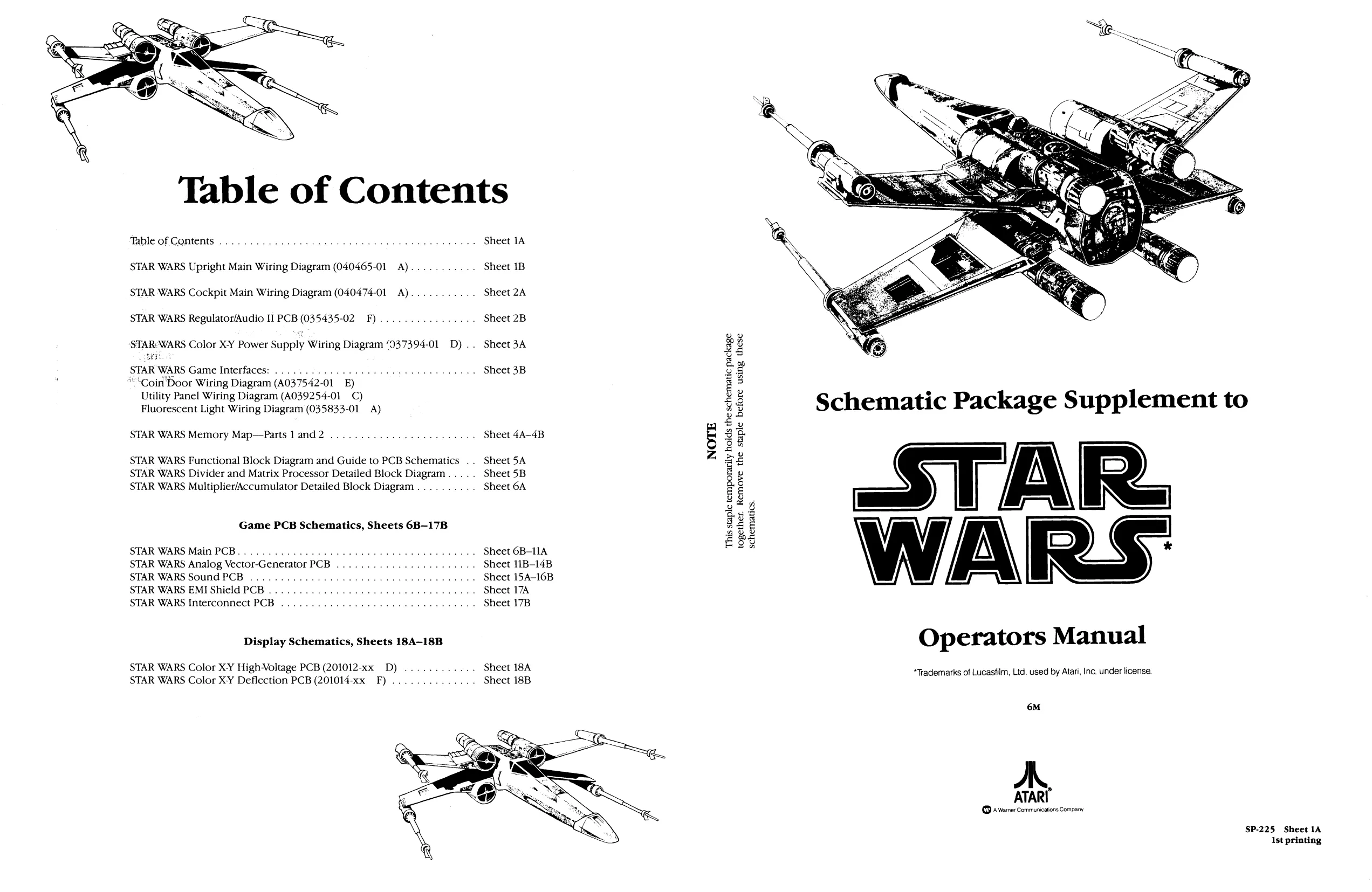
Table of Contents
Table OF GOREN wis os ce cee eoaas HL ede HAS U Os Nema HEE Sheet 1A
STAR WARS Upright Main Wiring Diagram (040465-01 A)... ..... Sheet 1B
STAR WARS Cockpit Main Wiring Diagram (040474-01 A)........... Sheet 2A
STAR WARS Regulator/Audio II PCB (035435-02 F)..... teeeeeeee. Sheet 2B
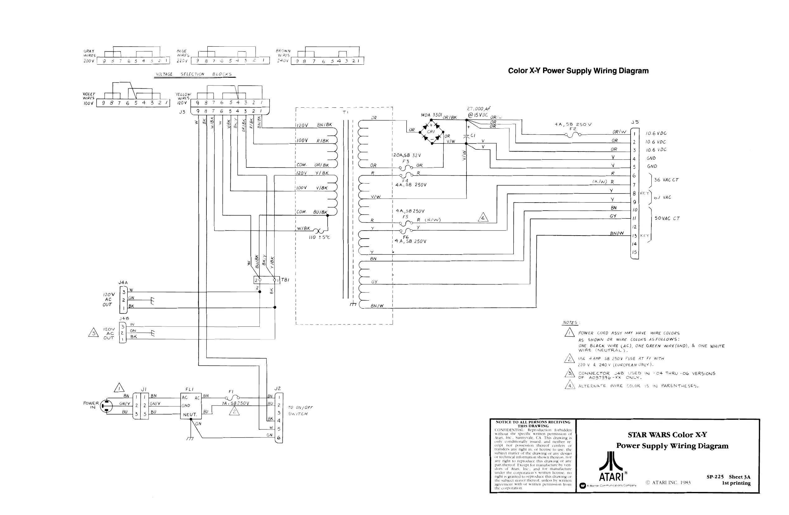
STAR: WARS Color X-Y Power Supply Wiring Diagram ‘037394-01 D).. Sheet 3A
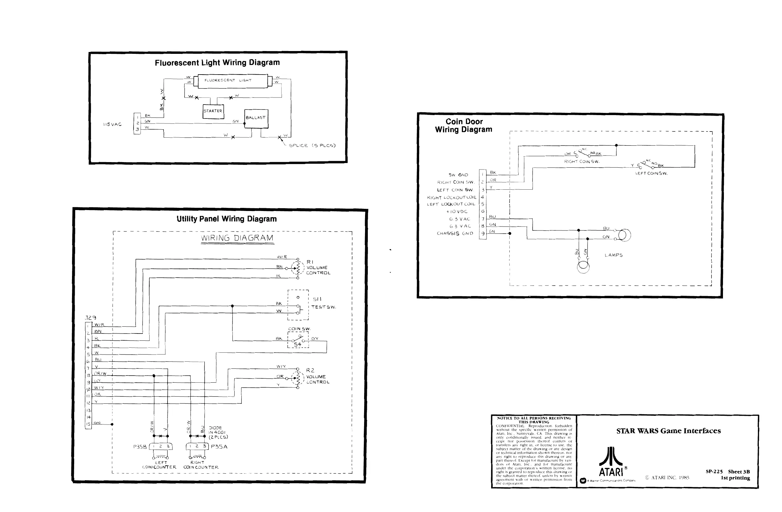
STAR WARS Game Interfaces: .............- ves Sone 3 seveeeeee. Sheet 3B *‘Coin Door Wiring Diagram (A037542-01_E) Utility Panel Wiring Diagram (A039254-01 C) Fluorescent Light Wiring Diagram (035833-01 A)
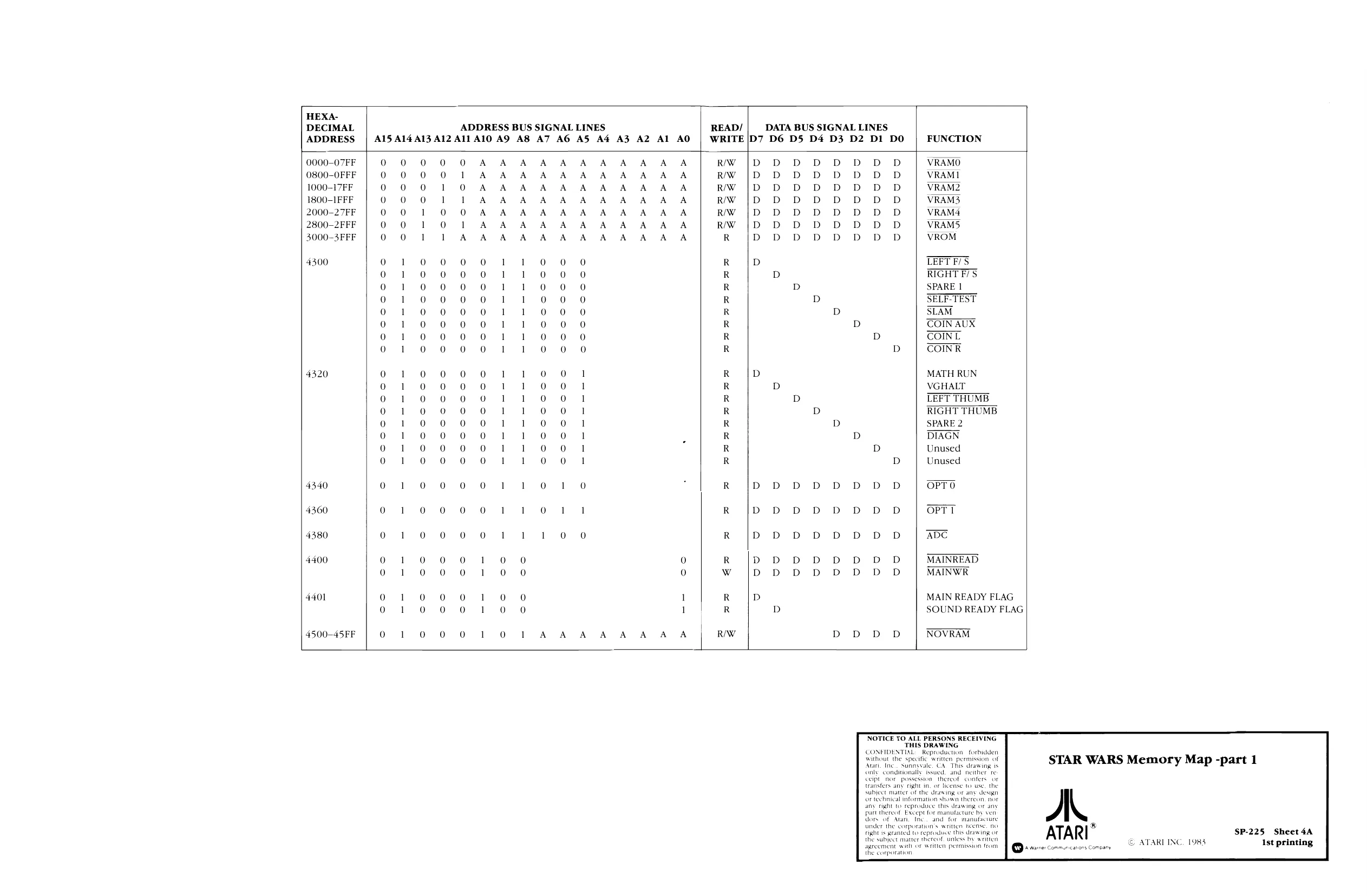
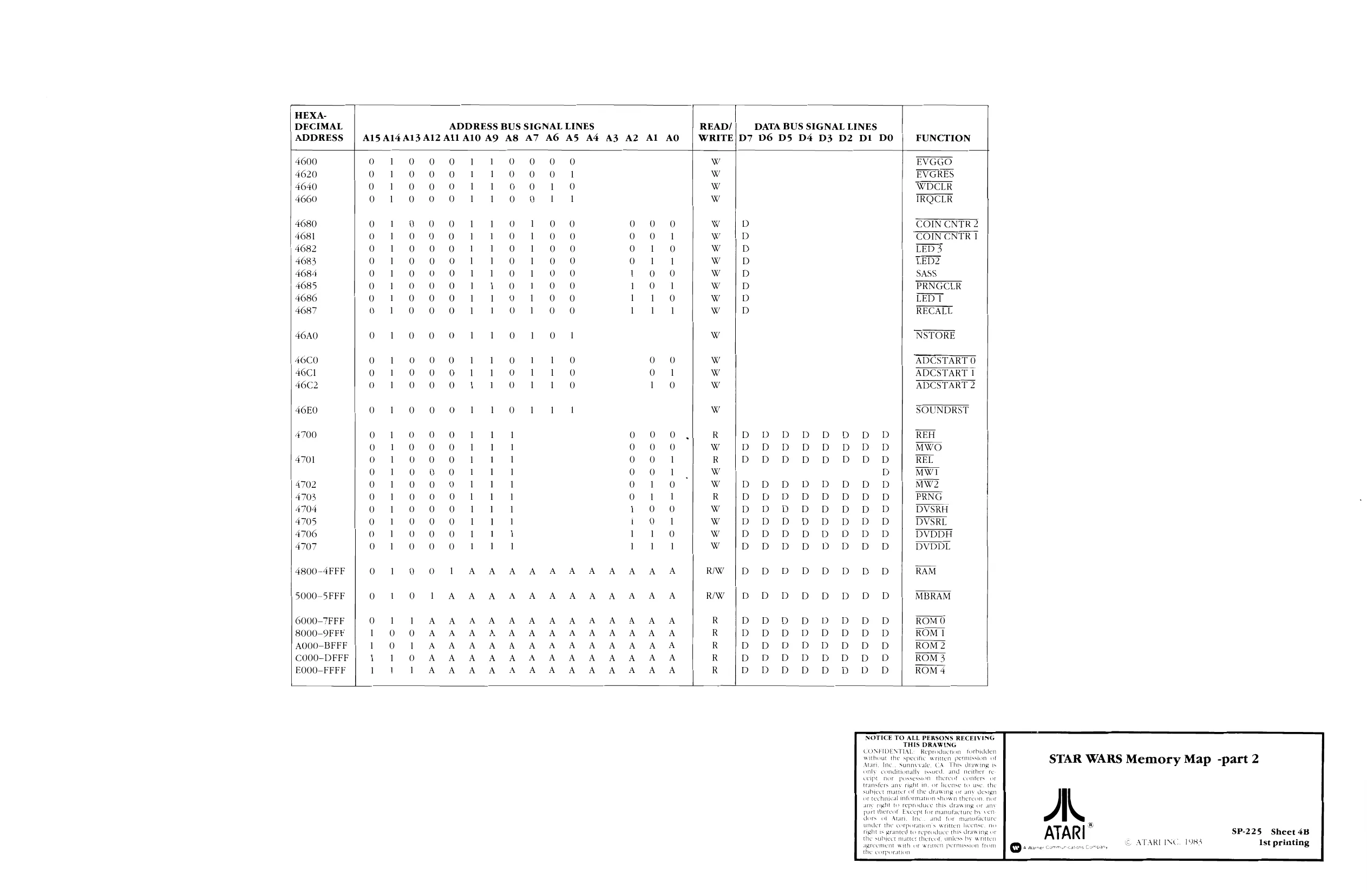
STAR WARS Memory Map—Parts land2 ............... sseee.s. Sheet 4A-4B
STAR WARS Functional Block Diagram and Guide to PCB Schematics .. Sheet 5A STAR WARS Divider and Matrix Processor Detailed Block Diagram..... Sheet 5B STAR WARS Multiplier/Accumulator Detailed Block Diagram ........ . Sheet 6A
Game PCB Schematics, Sheets 6B-17B
STAR WARS Main PCB................ ie STAR WARS Analog Vector-Generator PCB ... STAR WARS Sound PCB . ches Sheet 6B-11A. . Sheet 11B-14B . Sheet 15A-16B STAR WARS EMI Shield PCB fee .. Sheet 17A STAR WARS Interconnect PCB ........ . Sheet 17B
Display Schematics, Sheets 18A-18B
STAR WARS Color X-Y High-Voltage PCB (201012-xx D) ............ Sheet 18A STAR WARS Color XY Deflection PCB (201014-xx F) ............. Sheet 18B
schematics. Schematic Package Supplement to
STAR WARS:
Operators Manual
*Trademarks of Lucasfilm, Ltd. used by Atari, Inc. under license.
6M
ATARI © A Warner Communications Company
SP-225 Sheet 1A 1st printing
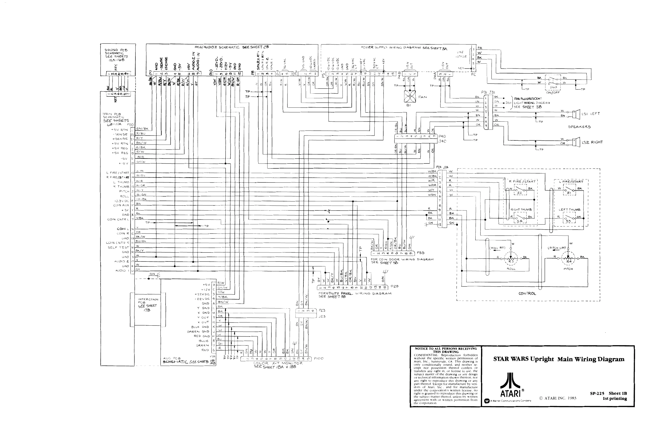
This page is a drawing, shown as the original scan.
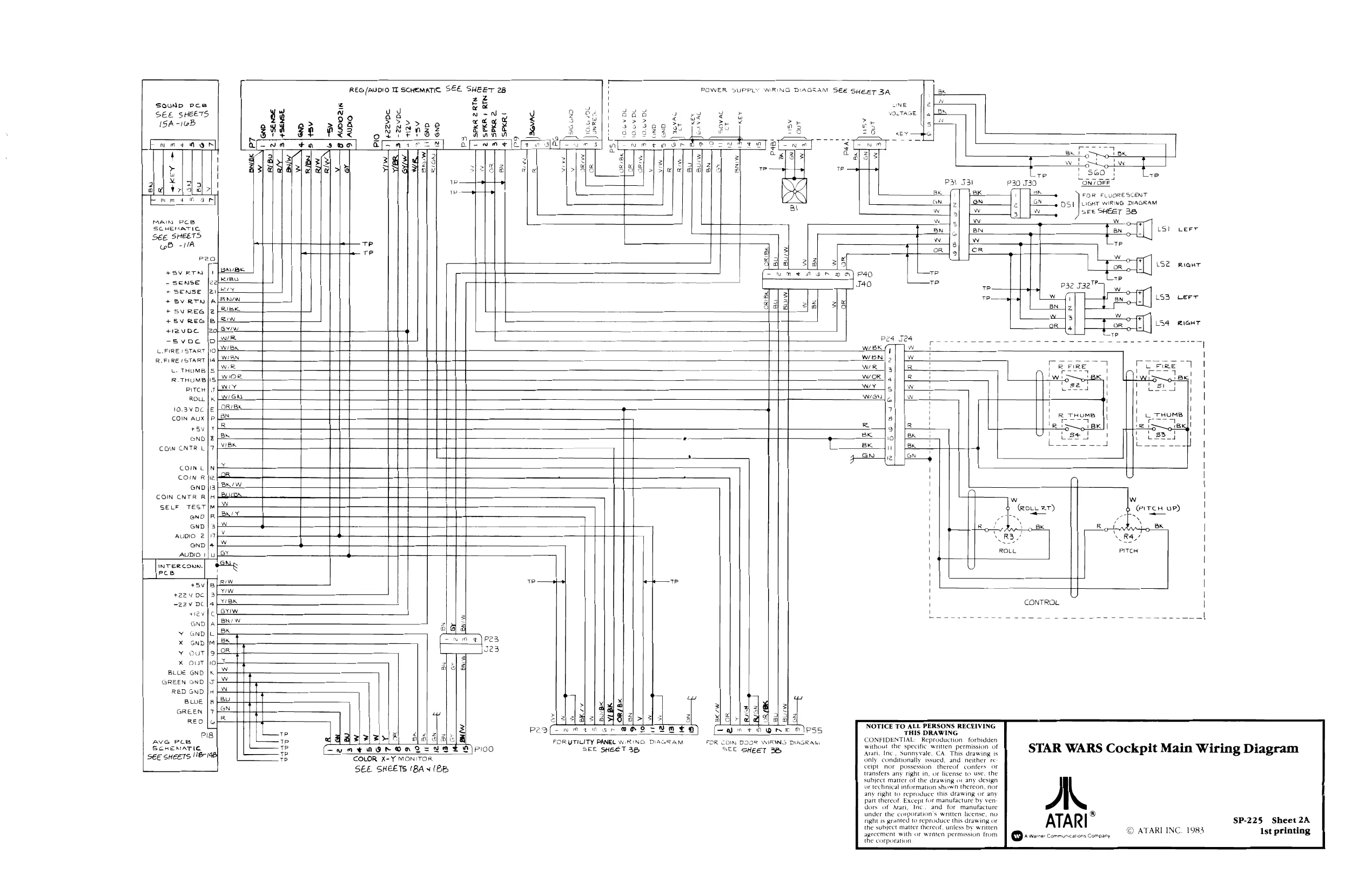
This page is a drawing, shown as the original scan.
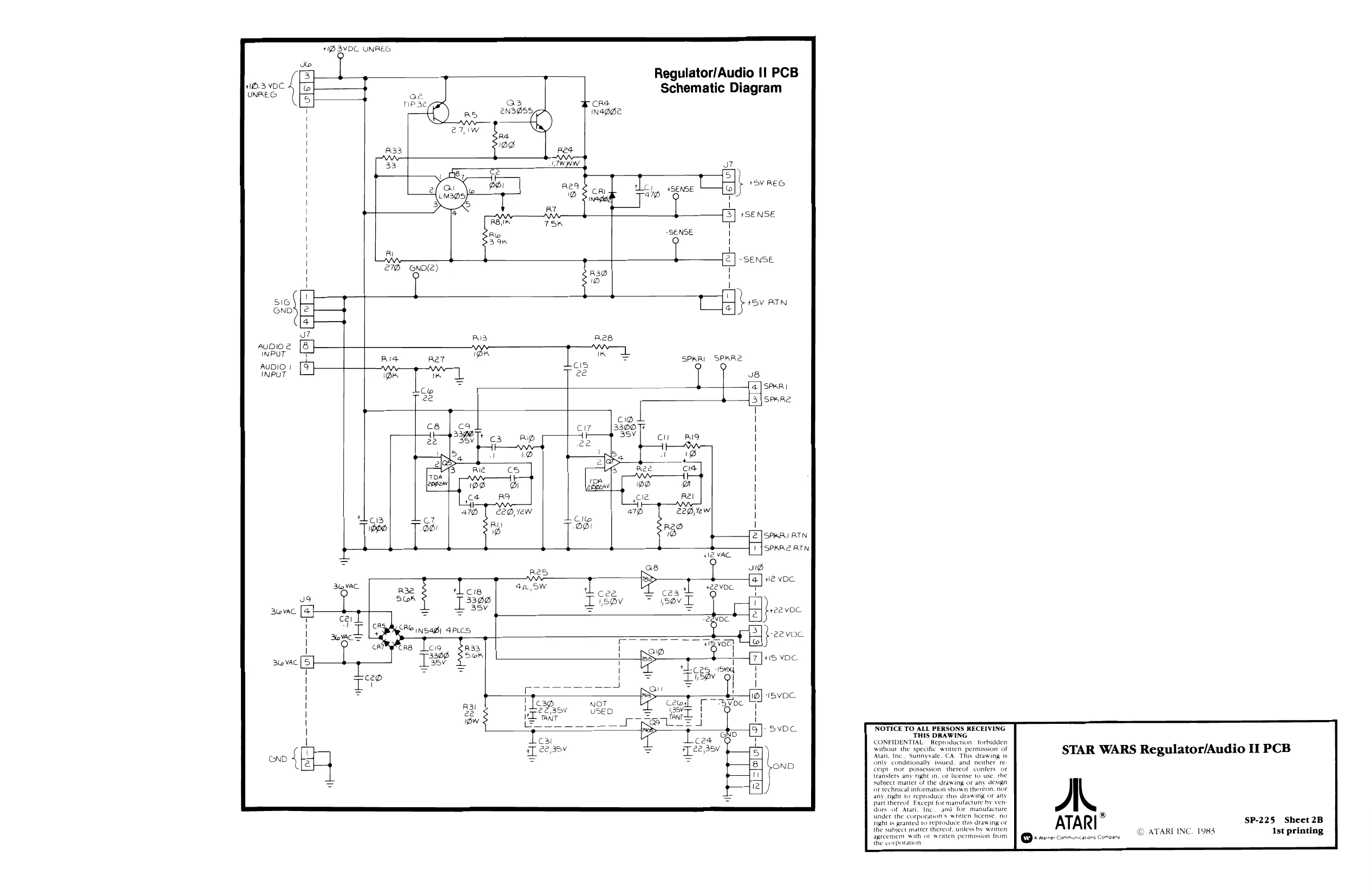
This page is a drawing, shown as the original scan.
This page is a drawing, shown as the original scan.
This page is a drawing, shown as the original scan.
This page is a drawing, shown as the original scan.
This page is a drawing, shown as the original scan.
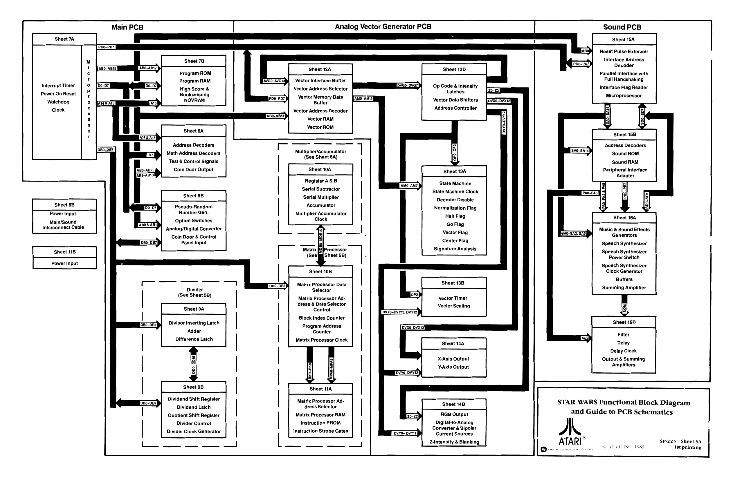
Main PCB
‘Sheet 7A
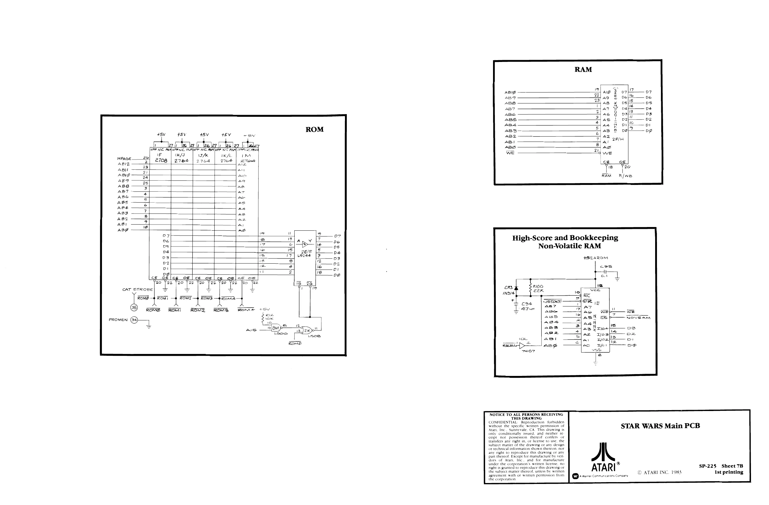
Sheet 78
Program ROM Program RAM
Interrupt Timer [50-07] High Score & Watchdog NOVRAM
Power On Reset Bookkeeping
Clock
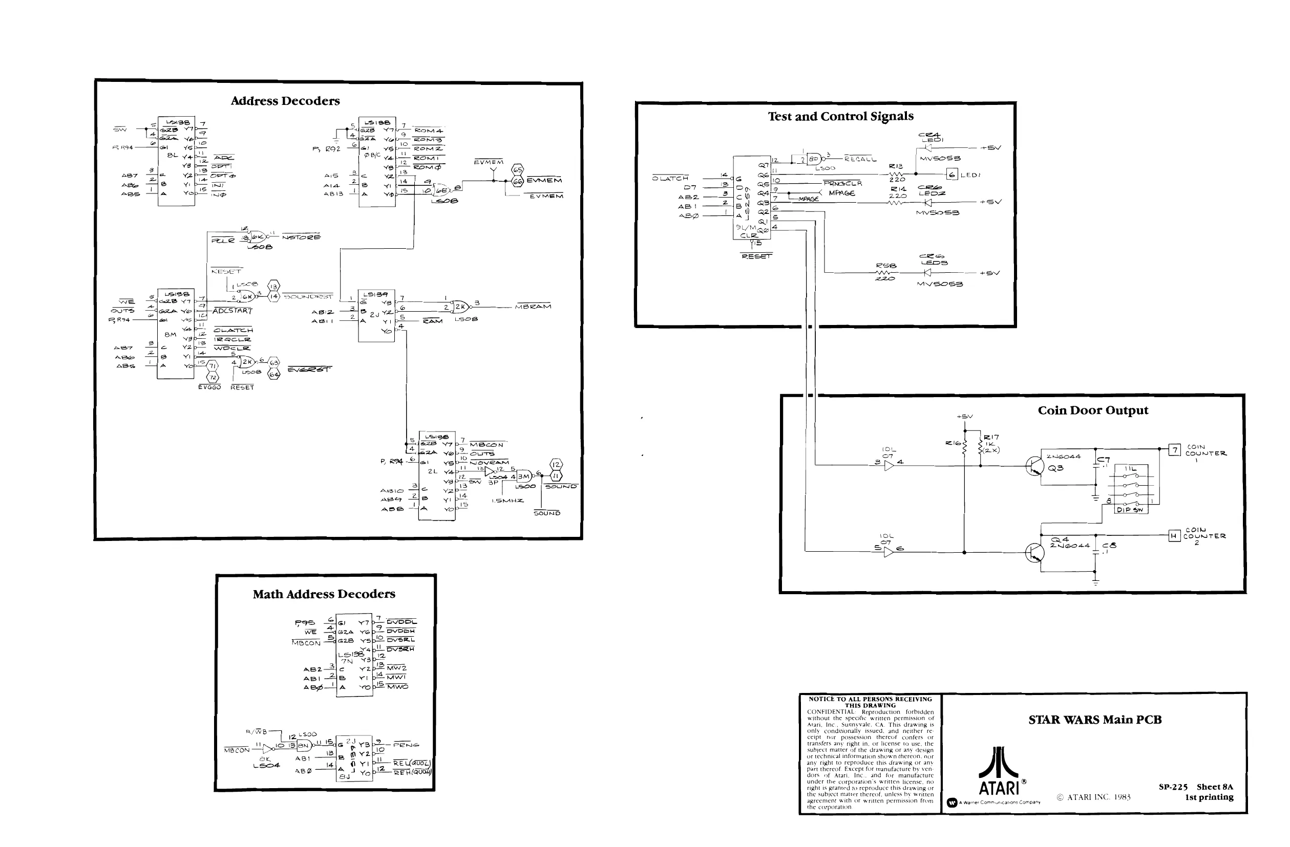
Address Decoders
Math Address Decoders
Test & Control Signals
Coin Door Output
ABO-AB2, BS-ABI
Sheet 8B
Pseudo-Random Number Gen. Power Input
Main/Sound Interconnect Cable
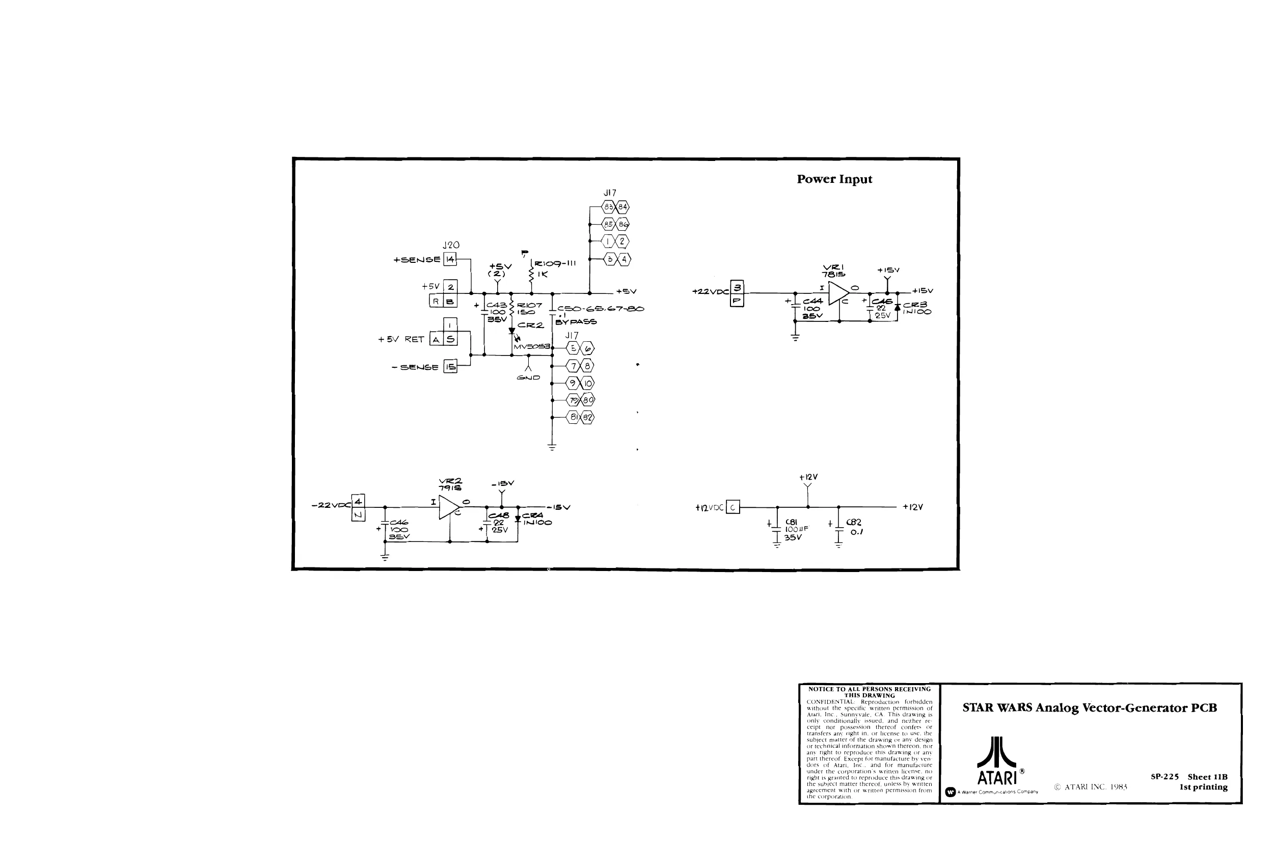
Sheet 11B
Power Input .
Option Switches
Analog/Digital Converter Coin Door & Control
[bB0-087 Panel Input
rc Divider (See Sheet 58)
Sheet 9A
Divisor Inverting Latch Adder
Difference Latch
Dividend Shift Register
Dividend Latch
Quotient Shift Register Divider Control
Divider Clock Generator Analog Vector Generator PCB
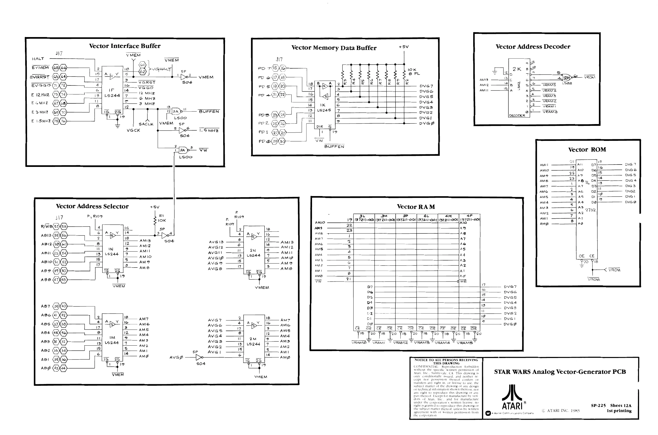
Vector Interface Bufter
Vector Address Selector [AVGO-AVGT3)
Vector Memory Data Buffer
Vector Address Decoder
Vector RAM
Vector ROM
Multiplier/Accumulator 7 (See Sheet 6A)
Serial Subtractor
Serial Multiplier Accumulator Register A & B |
Multiplier Accumulator |
B0-MDBIS Matrix [2|Processor (See gl Sheet 5B)
Matrix Processor Data Selector
Matrix Processor Address & Data Selector Control
Block Index Counter
Program Address Counter
Matrix Processor Clock
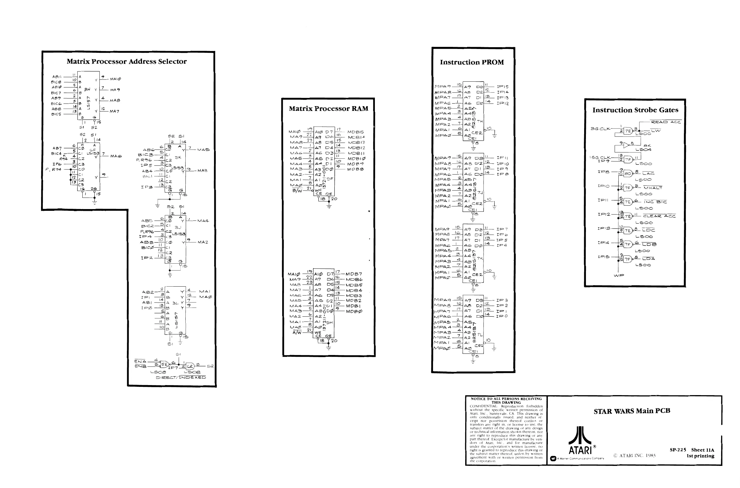
dress Selector
Matrix Processor RAM
Instruction PROM
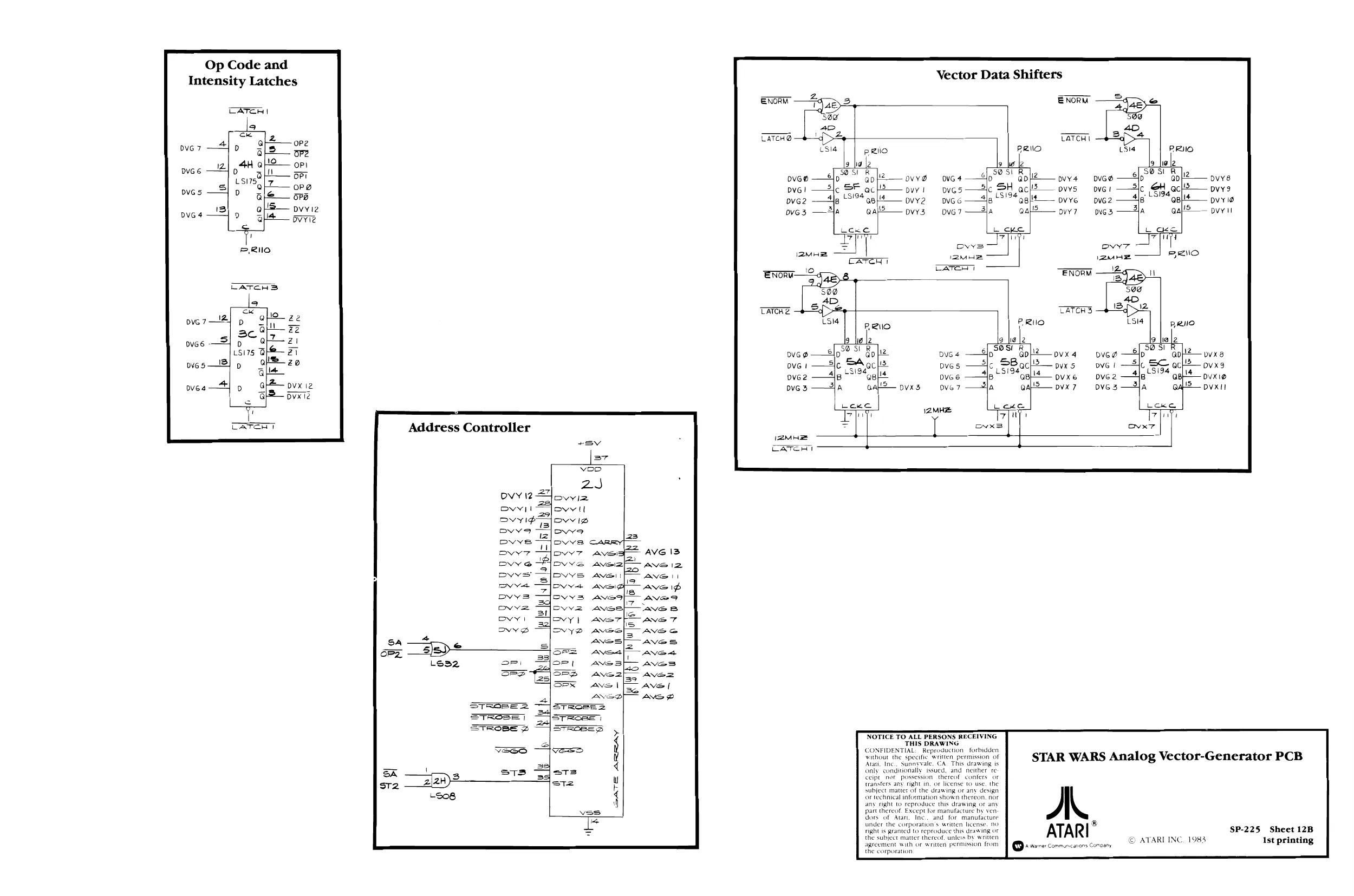
instruction Strobe Gates | Matrix Processor Ad- Op Code & Intensity Latches
Vector Data Shifters
Address Controller
State Machine
State Machine Clock
Decoder Disable
Normalization Flag
Halt Flag
Go Flag Vector Flag Center Flag Signature Analysis
Sheet 13B
Vector Timer
Vector Scaling
DVX0_DVX12)
Sheet 144
X-Axis Output Y-Axis Output
Sheet 14B
RGB Output Digital-to-Analog Converter & Bipolar Current Sources [ ovvo- pvvii | Z-Intensity & Blanking O-vre coy © ATAREING. 1983 Sound PCB
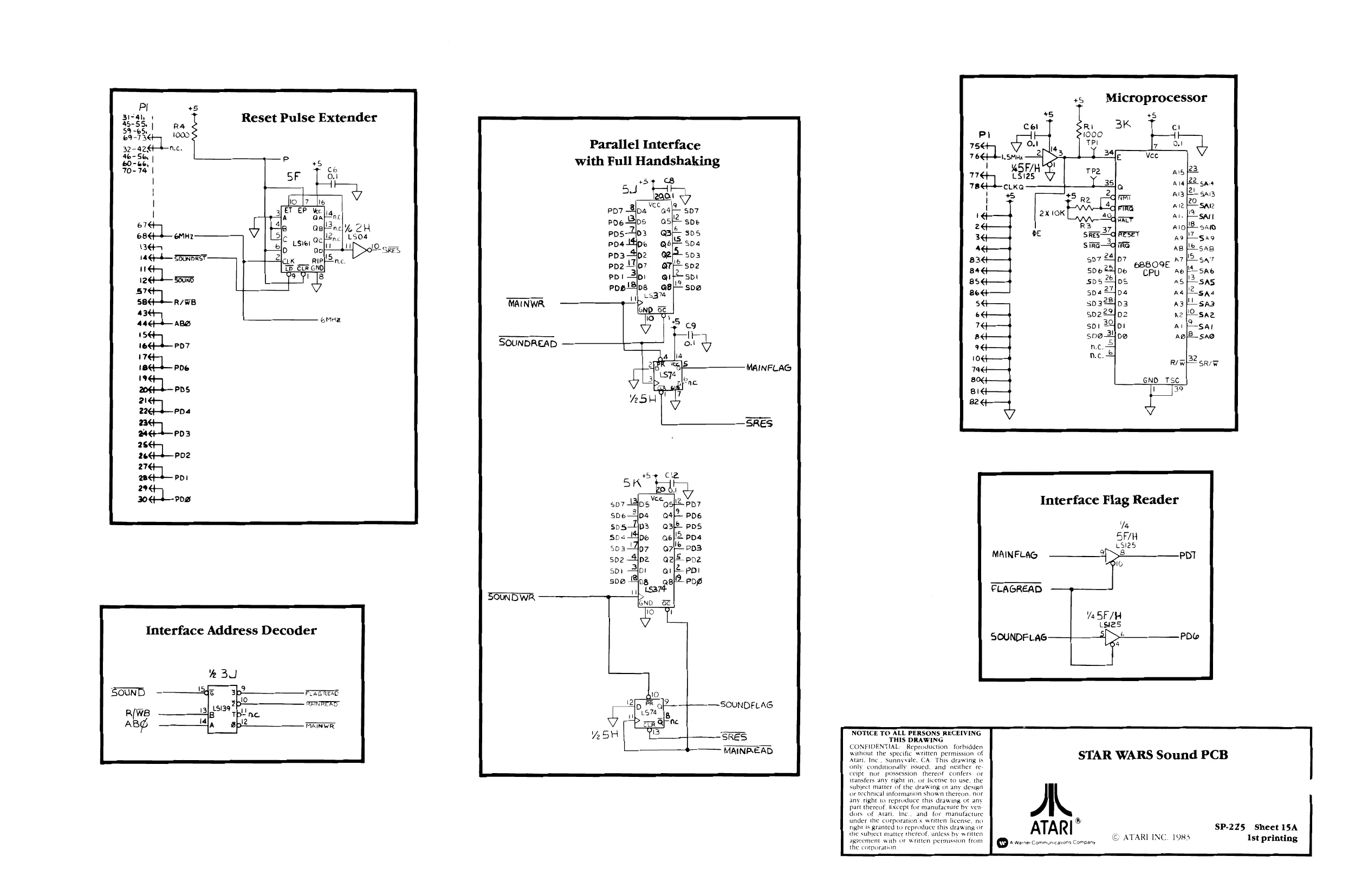
Reset Pulse Extender
Interface Address Decoder
Parallel Interface with Full Handshaking
Interface Flag Reader
Microprocessor
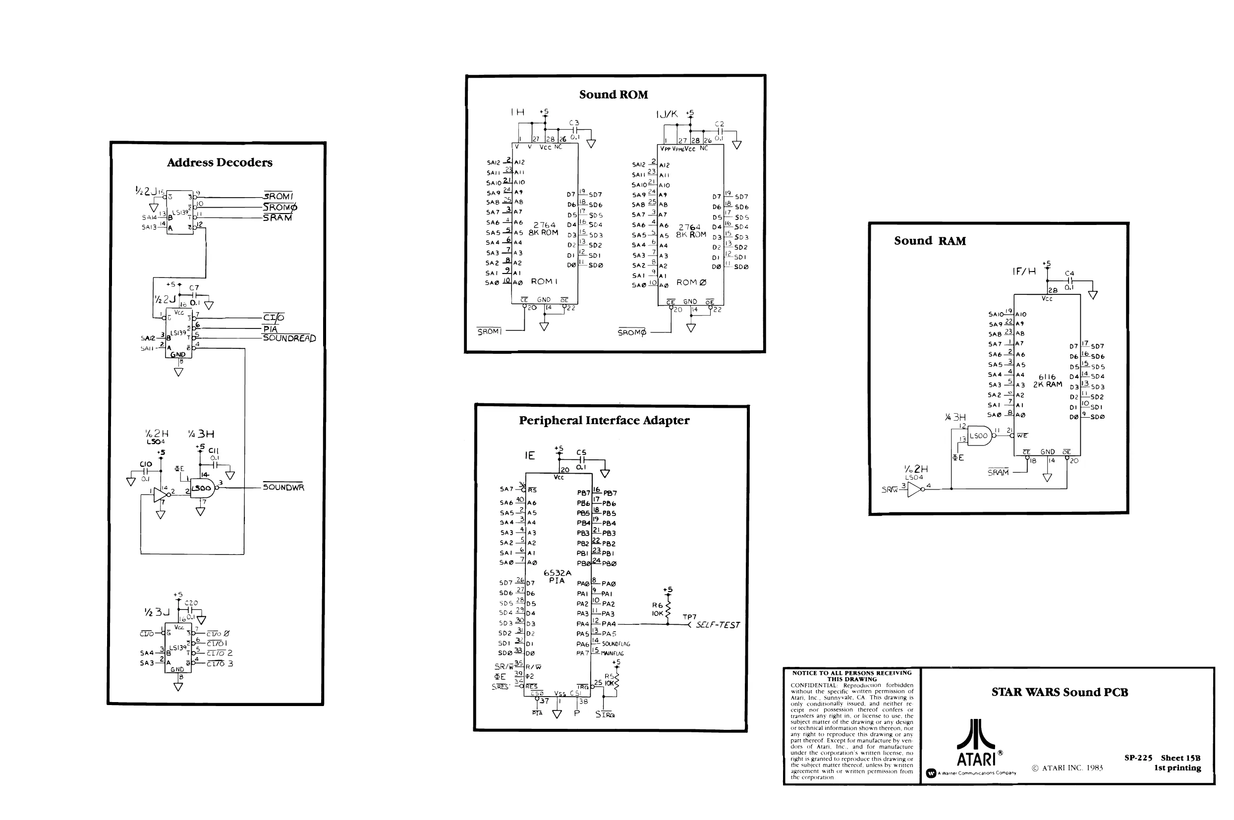
Address Decoders
Sound ROM
Sound RAM
Peripheral Interface Adapter
Music & Sound Effects Generators
Speech Synthesizer Speech Synthesizer Power Switch
Speech Synthesizer Clock Generator
Buffers
Summing Amplifier
Sheet 168
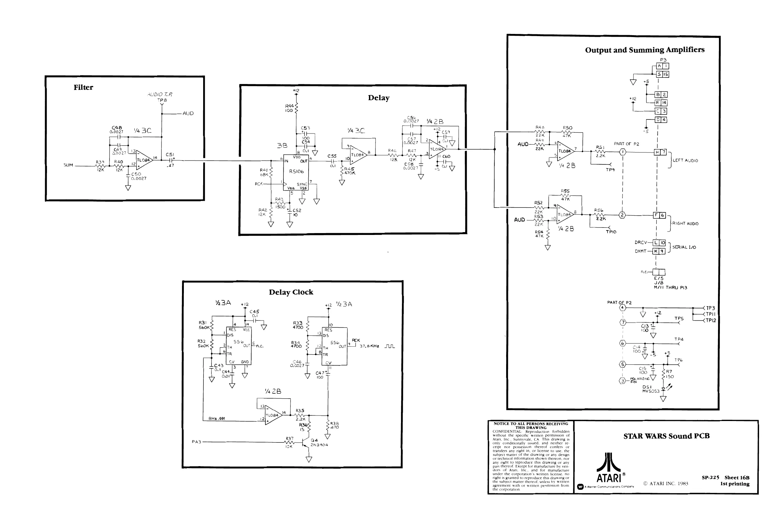
Filter
Delay Delay Clock Output & Summing Amplifiers
STAR WARS Functional Block Diagram and Guide to PCB Schematics AL
SP-225 Sheet 5A Ist printing
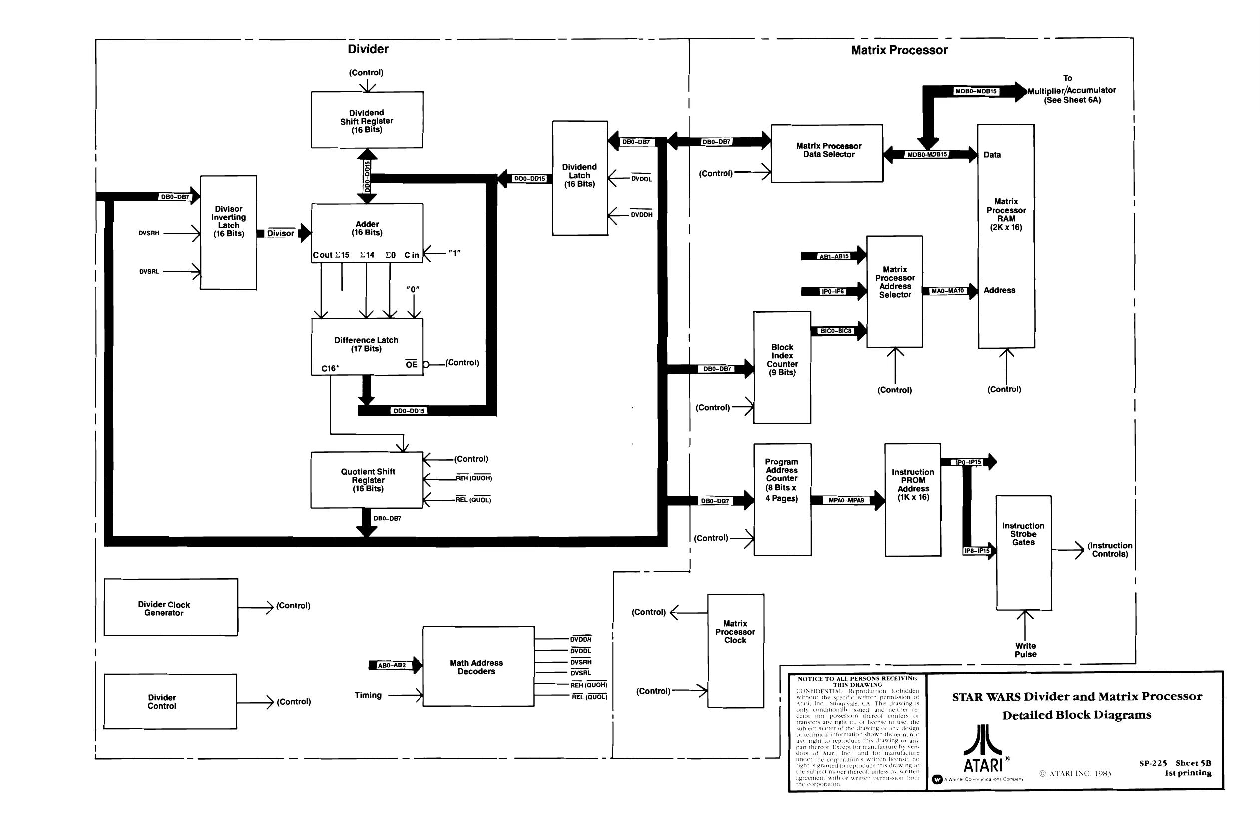
DB0-DE7
Divisor Inverting Latch
ovsRH (16 Bits)
DVSRL
Divider Clock (Control) Generator
Divider (Control)
Control
Divider
(Control)
Dividend Shift Register (16 Bits)
Adder (16 Bits)
Coutli5 £14 +o
Difference Latch (17 Bits)
C16"
Quotient Shift Register (16 Bits)
Timing Dividend Latch (16 Bits)
‘OVDDR DvDDL OVvSRH DVSRL REH (QUOR) FEL (@UOT} Math Address Decoders (Control)
(Control) [DB0-DB7
(Controf)
(B0_DB7
(Control) (Control) a,
Matrix Processor
To jultiplier/Accumulator (See Sheet 6A)
Data Selector Data
Matrix i Processor RAM (2Kx 16)
Matrix Lt nimeel Address [1P0-1F5] Selector (MMAD-HAT Wy Address
Block Index Counter (9 Bits) (Control) (Controt)
Program
Address Instruction
Counter PROM
(8 Bits x Address | 4 Pages) (1K x 16)
Instruction Strobe Gates (instruction Controls)
I
NOTICE TO ALL PERSONS RECEIVING THIS DRAWING CONFIDENTIAL: Reproduction forbidden without the specific written permission of Atari, Inc., Sunnyvale, CA This drawing 1s only conditionally issued, and. neither re Ceipt “AOE possession thereat confers or transfers ant right iN. oF license to use, the Subject maatter of the drawing or any design Gr technical mtormation shown thereon, not any right to reproduce this drawing oF any fart thereof Except for manufacture by ven. Goes of Atari and for manufacture under the corporation s written license, 10 bt is granted to reproduce this drawing or the subject mater thereat. unless be watten, agreement with oe written permIssion trom, the corporation A. ATARI . STAR WARS Divider and Matrix Processor
Detailed Block Diagrams
© ATARI ING. 1983 SP-225 Sheet 5B Ist printing
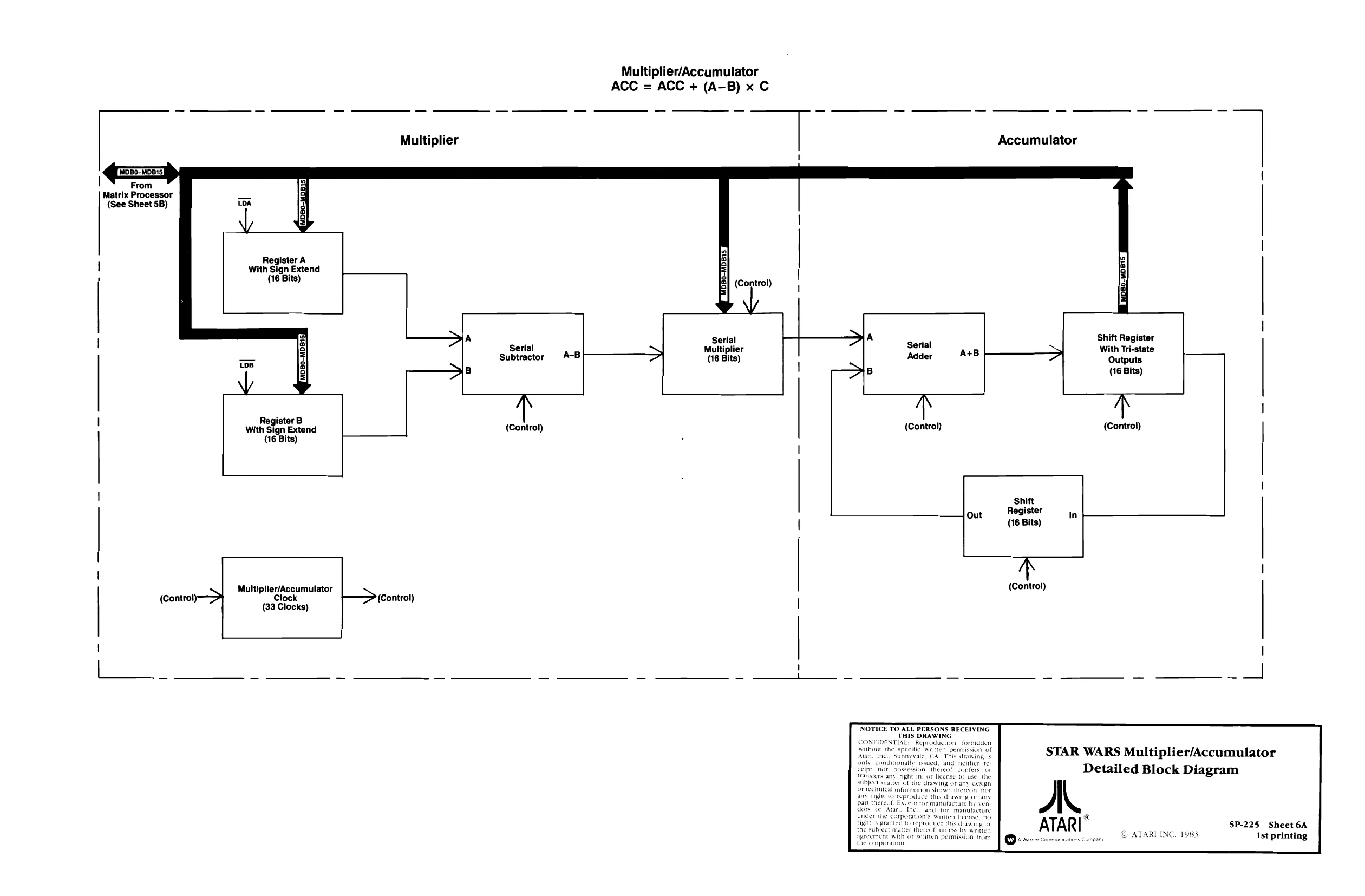
This page is a drawing, shown as the original scan.
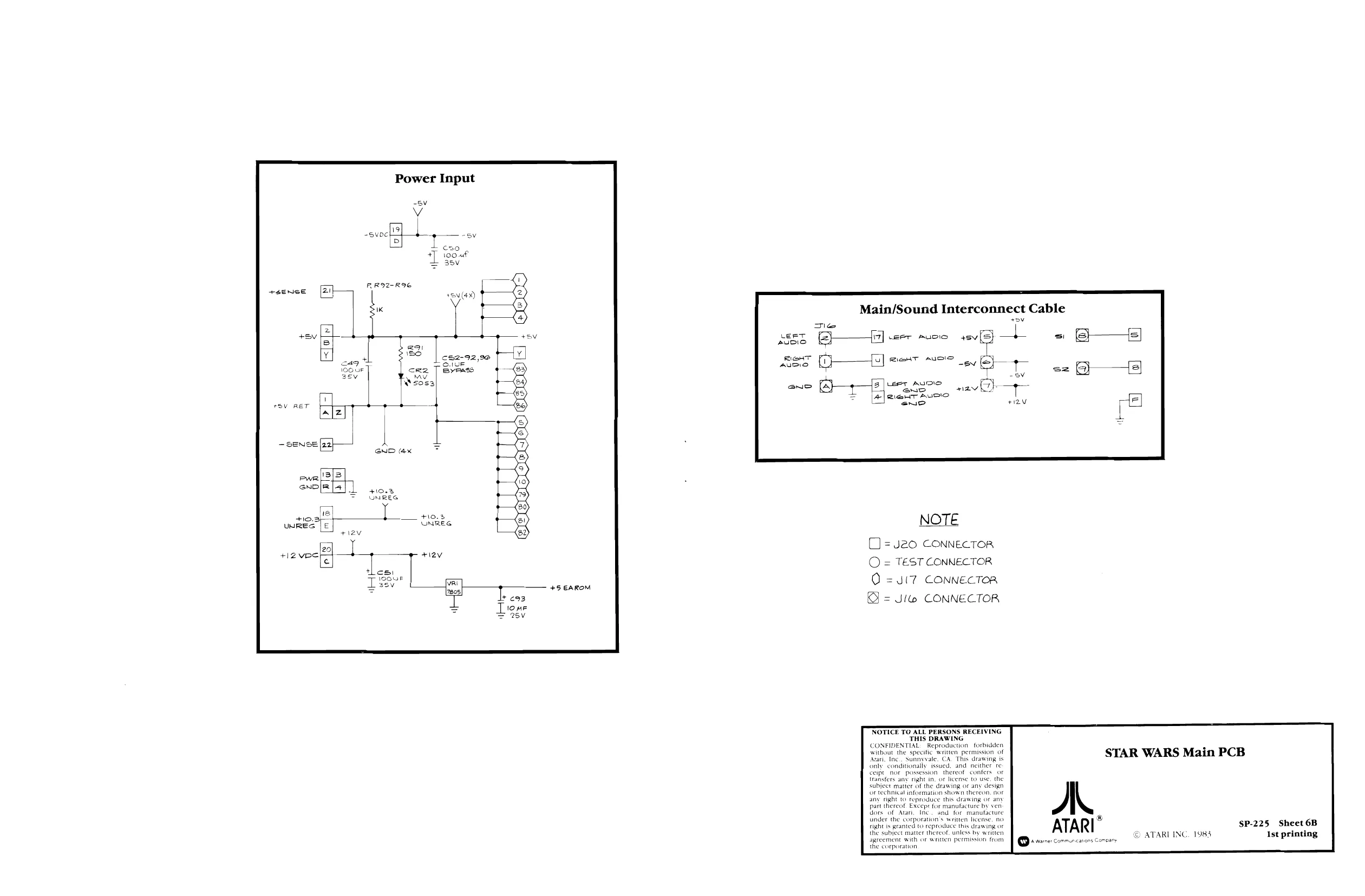
This page is a drawing, shown as the original scan.
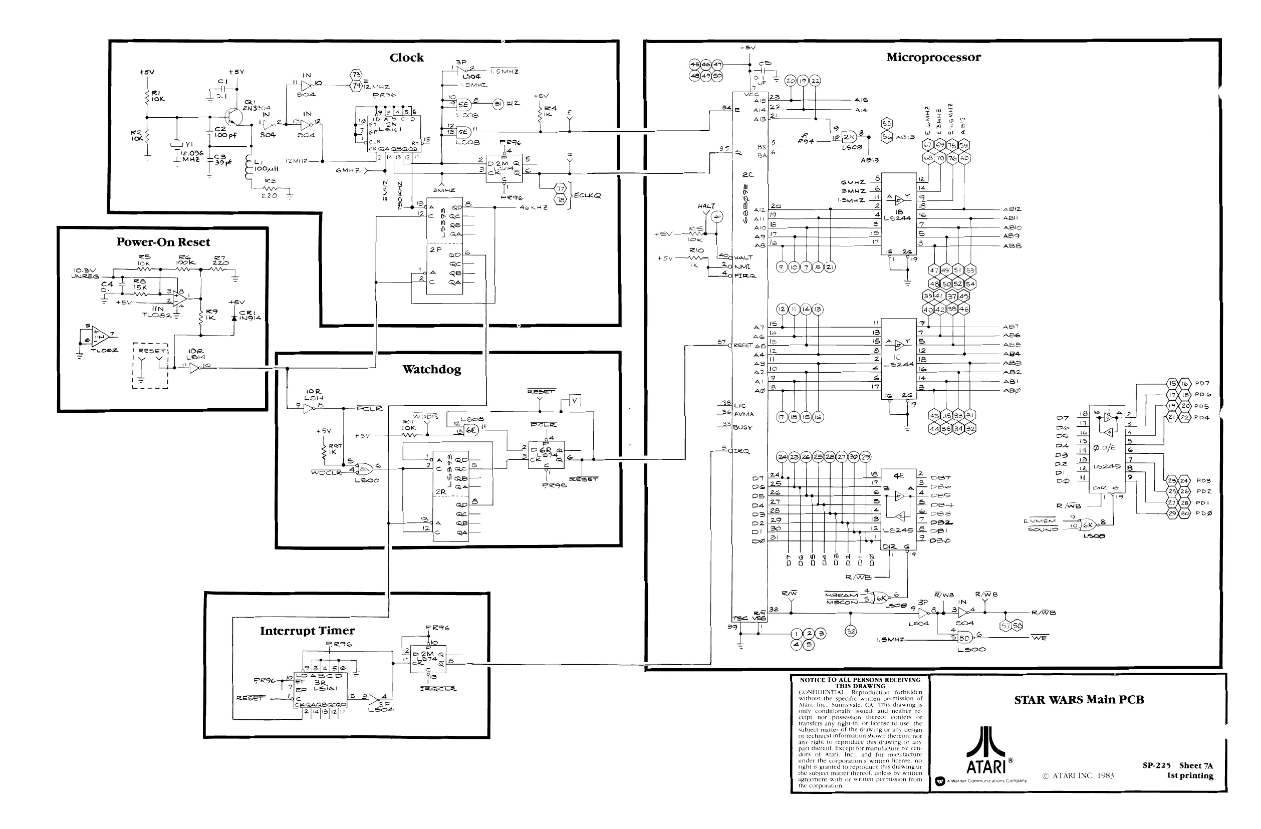
Power-On Reset
es lox ze B)
Clock
PRO
Oanean
Ltyeve wae CD Bee “ZN Tlerteter
cK RAQBAceR Re
2 [ia
eMHz epe[y
Microprocessor
Watchdog
WED eu OK. si
Interrupt Timer
a
ABD ~
AG: ABS RESET as] 1B nee
| AS f ABA
ex ABS aztt aaz
Al AS! POT
- ase RB oo
NOTICE TO ALL PERSONS RECEIVING THIS DRAWING. CONFIDENTIAL: Reproduction forbidden without the specific written permission of Atari, Inc,. Sunnyvale, CA. This drawing. Is nly conditionally issued. and neither re cept nor possession thereof confers or transfers any fightin. or license to use, the subject matter of the drawing or any design Or technical information shown thereon, not any right to reproduce this drawing or anv part thereof Except for manufacture by ven. dors of Atari, Inc, and for manufacture under the corporation's weitten license, no.
fight is granted to reproduce this drawing or
the subject matter thereot. unless by written agreement with of silken permission from, the corporation, STAR WARS Main PCB
AN ATARI SP-225 Sheet 7A Oe rvvee sovscompay © ATARLINC. 1985 Ist printing,
This page is a drawing, shown as the original scan.
This page is a drawing, shown as the original scan.
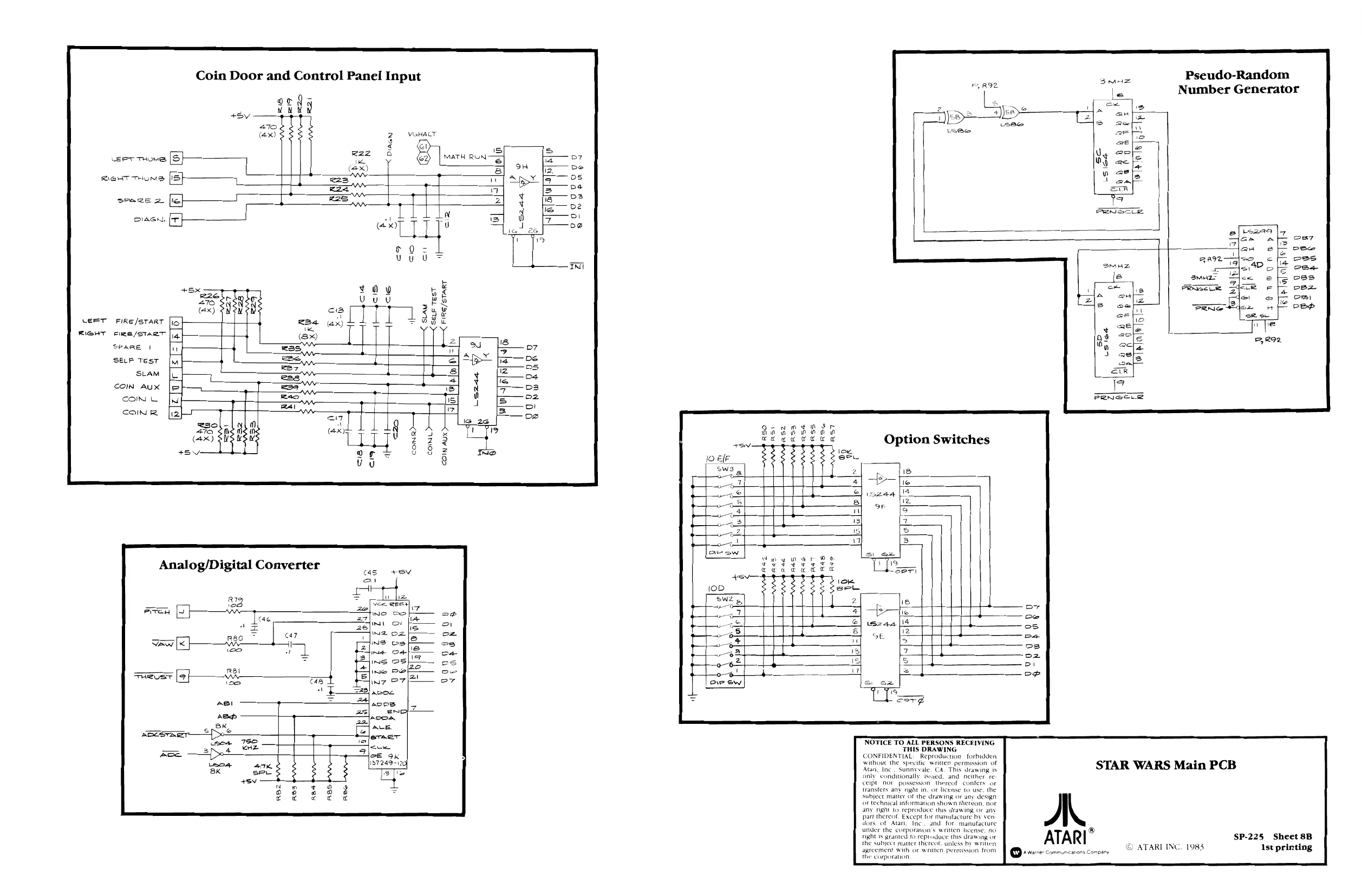
Coin Door and Control Panel Input
adi
eer THOS
RIGHT HUN
sece 2
DIAGH.
Ler Fike /sTaRT
RIGHT cme/stacT
SLAM
‘SELF TEST
$— Fire/start
SPARE |
SELF Test
COIN AUX
CON LL [OL foo] o}=[
COIN f
Pseudo-Random Number Generator
Option Switches
+e—Te iozes [IA
oF
z S
c as a
e
ele = z. fe eee fhe perme FER 6 fo z 1Z Bic ete Cel eo 86h PENS eden 4 CBP eR oe 7 (= Tofelals 51
NOTICE TO ALL PERSONS RECEIVING THIS DRAWING CONFIDENTIAL: Reproduction forbidden, without the specific written permission of Atul, Inc, Sunnyvale, CA. This deawing is only’ conditionally issued, and neither re Ceipt_ nor possession thereof confers or transfers any right in, oF license w use, the subject matter oF the drawing or any design of technical information shown thereon, nor any right to reproduce this drawing Or any pare thereat Except for manufacture by ven. dors of Atari, Inc. and. for manufacture Under the corporauon's written license, 10. fight ts granted 10 reptoduce this drawing oF
the subject matter thereor unless by written,
agreement with of written Permission from, the corporation, STAR WARS Main PCB
A ATARI SP-225 Sheet 8B Qe vere: conmncatans company © ATARI INC. 1985 Ast printing
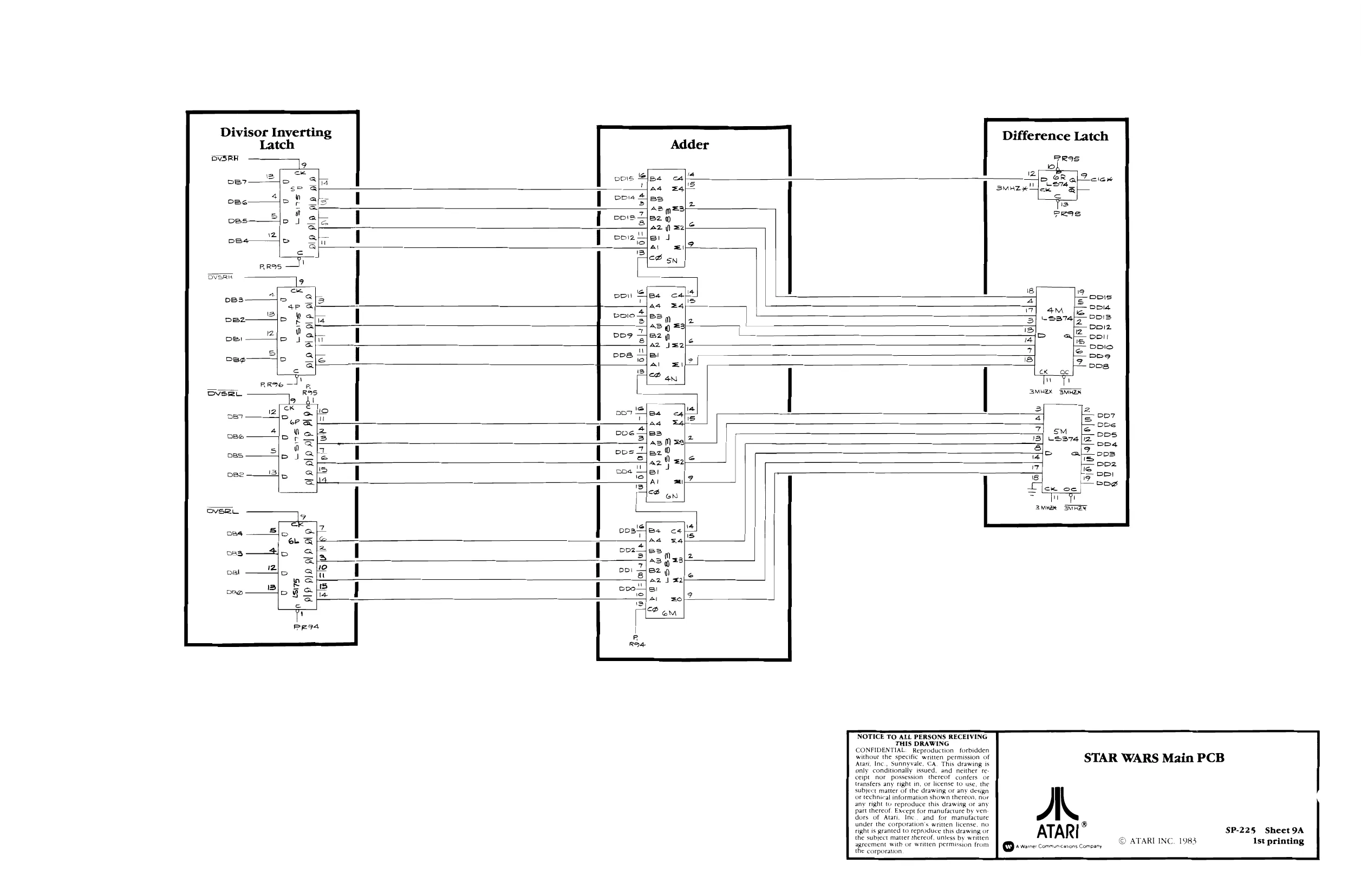
Divisor Inverting
Difference Latch
PRS
be7——4 DIP PID plo pia
DID PLP pip plo o_eRal Pcicn sunzxeeeael s 3S Peas
8 9 = Zoos 7] 4M opi 3] -sarat ons De S| 2 me afZ oo 7 DDIS
- IF B59 Dos x oc Yh a. o~ oh OG] | af w usrs 1p O]P AIP ar
U | oo ol
spy Bz PIP DID plP al p
ln ts175
a ae n ry
NOTICE TO ALL PERSONS RECEIVING THIS DRAWING CONFIDENTIAL: "Reproduction forbidden without the specific written permission of Atari, Inc, Sunnyvale, CA. This drawing is only: conditionally issued, and neither te ceipt_nor possession thereo! confers or transfers any right in, or license to use, the subject matter of the drawing or any design or technical information shown thereon, noe any right tw reproduce this drawing or any part thereof. Except for manufacture by ven dors of Atari, Ine. and for manufacture tunder the corporation's written license, no
right is granted to reproduce this drawing oF
the subject matter thereof, unless by written
agreement with or weitten permission from the corporavon ATARI? 212126: Communications Company
STAR WARS Main PCB
ATARI INC. 1983 SP-225 Sheet 9A Ist printing
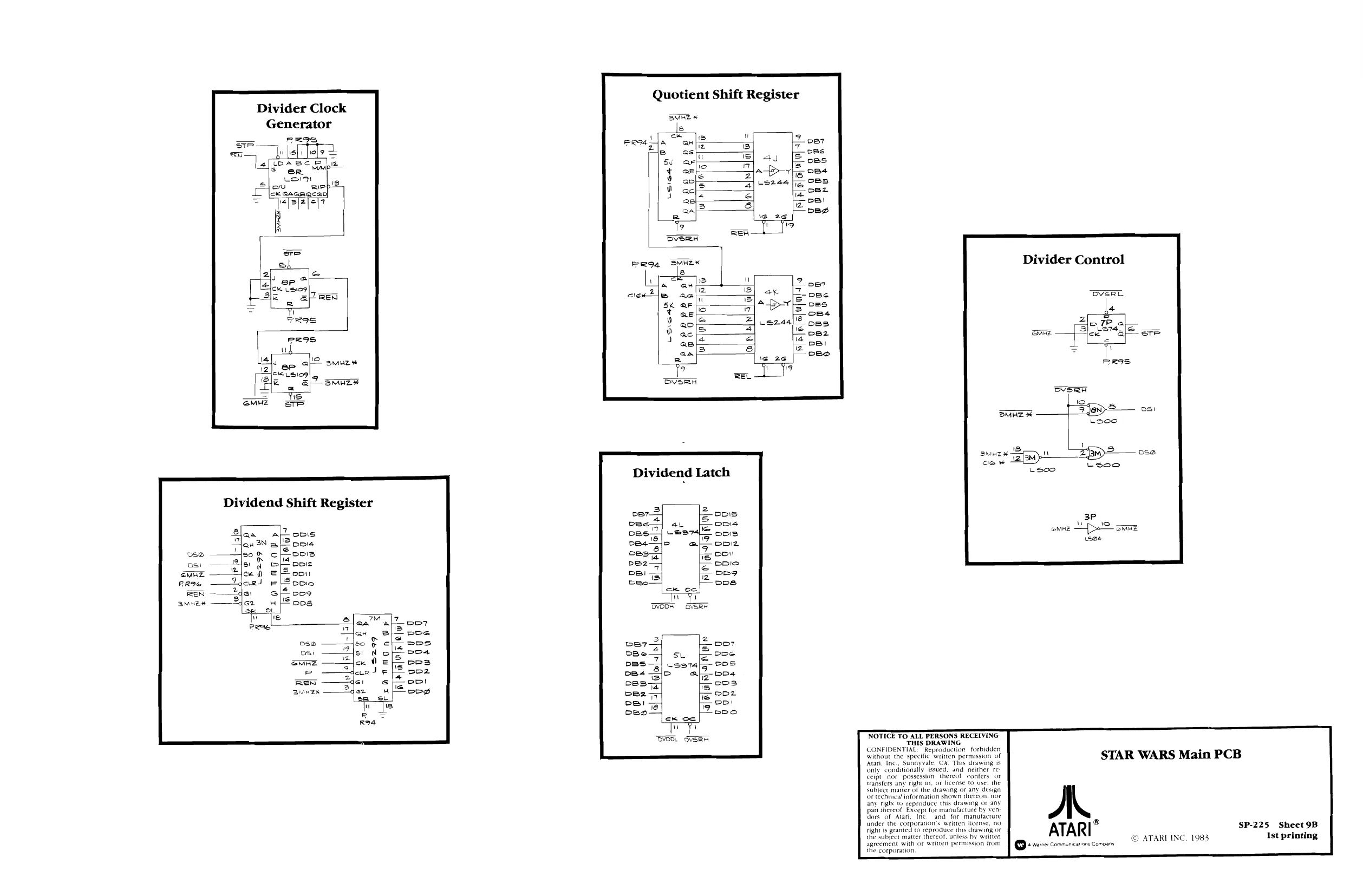
This page is a drawing, shown as the original scan.
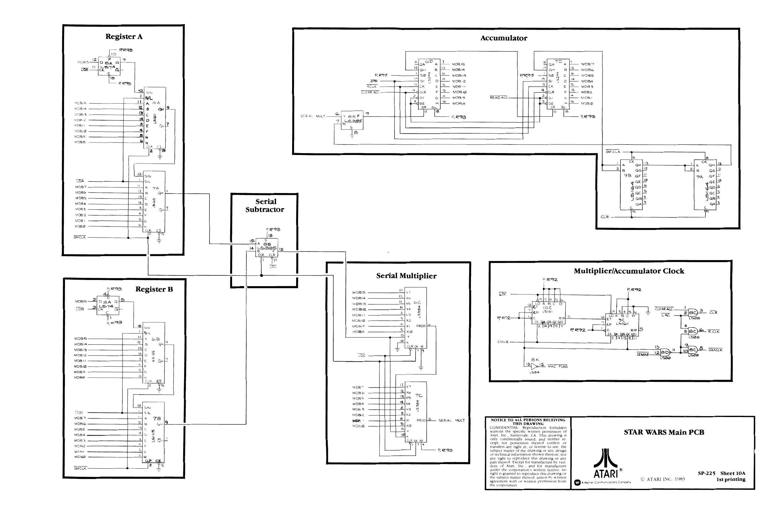
Register A Accumulator
- Peas
18 + 51
ra
TERRE. * cor wor READ AZ
Serial Subtractor
Tole lw le Te = Ie fp
Multiplier/Accumulator Clock
Serial Multiplier
Waitin Register B
MoBIS
Mpeia of |e [eke aoe eco ET 10 ep ss als roae oc quan gcae alee Se hapatetie EP Lele! e A Ge op on 2 T4313] Daa af& Aer _| Ti BIS MDE
wppie
Moe
MoRe
oR
moes
MoBia
OBIS
MoBi2
MOBI
MOBIa
MOBO
Moes,
Toe
MOB?
MOBG
Moss
mone serial wut NOTICE TO ALL PERSONS RECEIVING THIS DRAWING CONFIDENTIAL: "Reproduction forbidden without the specific written permission of STAR WARS Main PCB Atari, Inc., Sunnyvale, CA. This drawing is only conditionally issued, and neither re: Ceipt_nor possession thereof confers or transfers any right in, oF license 10 use. the subject matter of the urawing or any design Or technical information shown thereon, nor any right to reproduce this drawing or any part thereo! Except for manufacture by ven. Uors of Atari, Inc, and for manufacture Hh grasted to reproduce tis deswing oF ATARI ° SP-225 Sheet 10A the subject matter thereof, unless by written ee for written permission from YQ a marcer communications Comoany ATARI INC. 1983 Ist printing
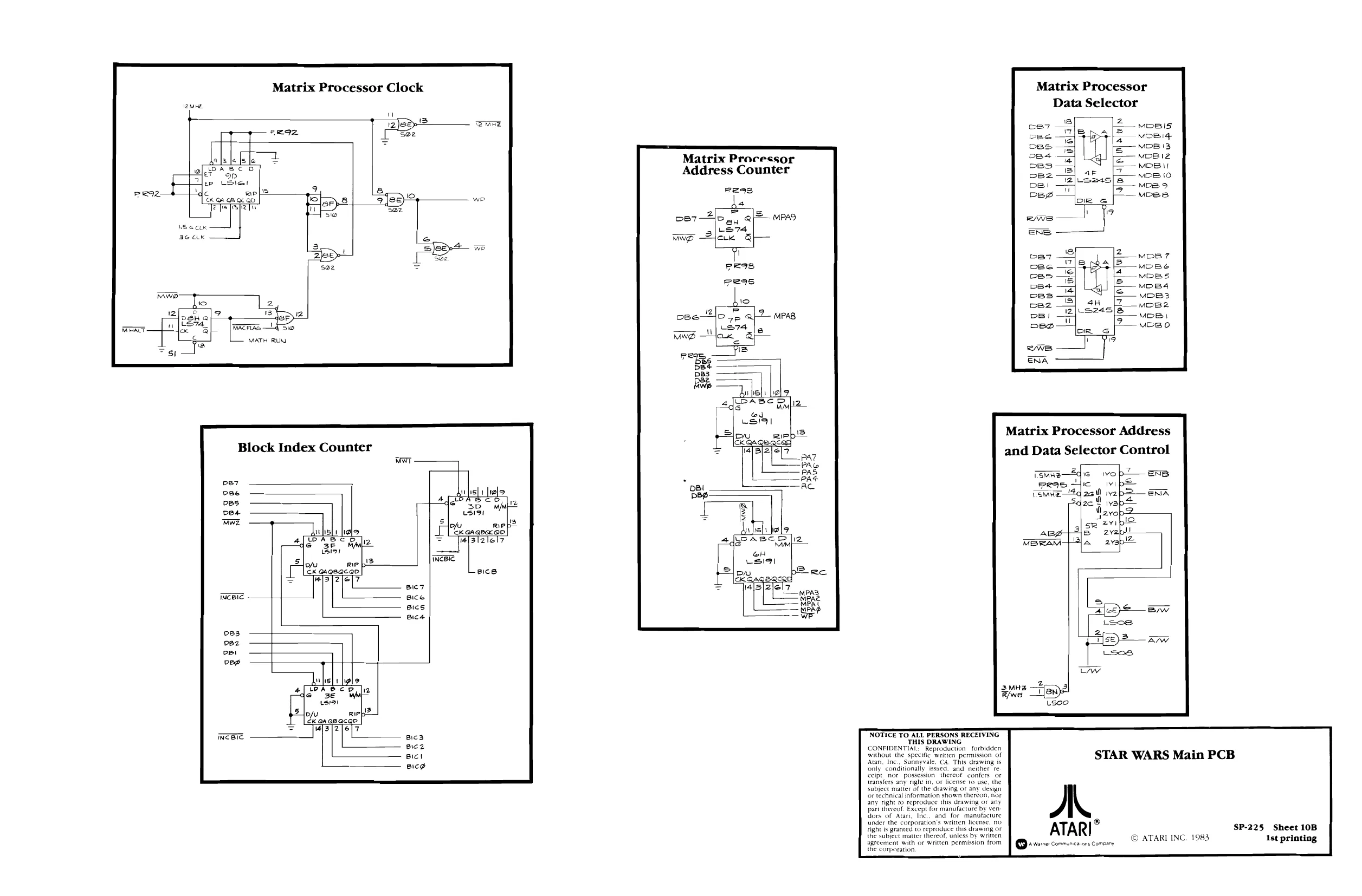
This page is a drawing, shown as the original scan.
This page is a drawing, shown as the original scan.
This page is a drawing, shown as the original scan.
This page is a drawing, shown as the original scan.
This page is a drawing, shown as the original scan.
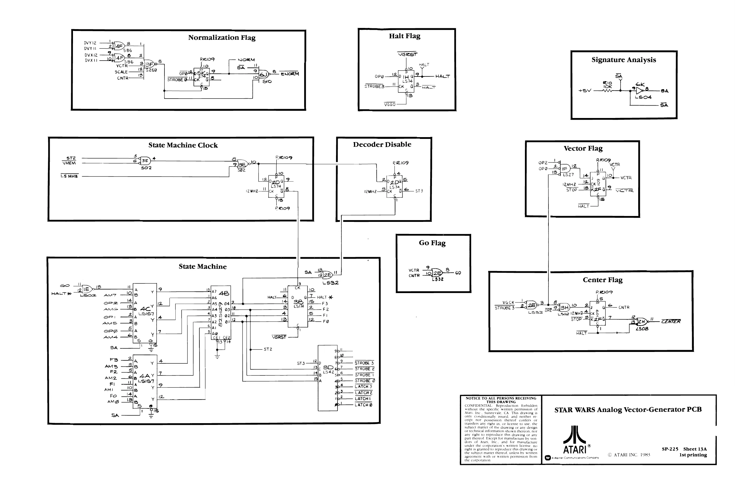
This page is a drawing, shown as the original scan.
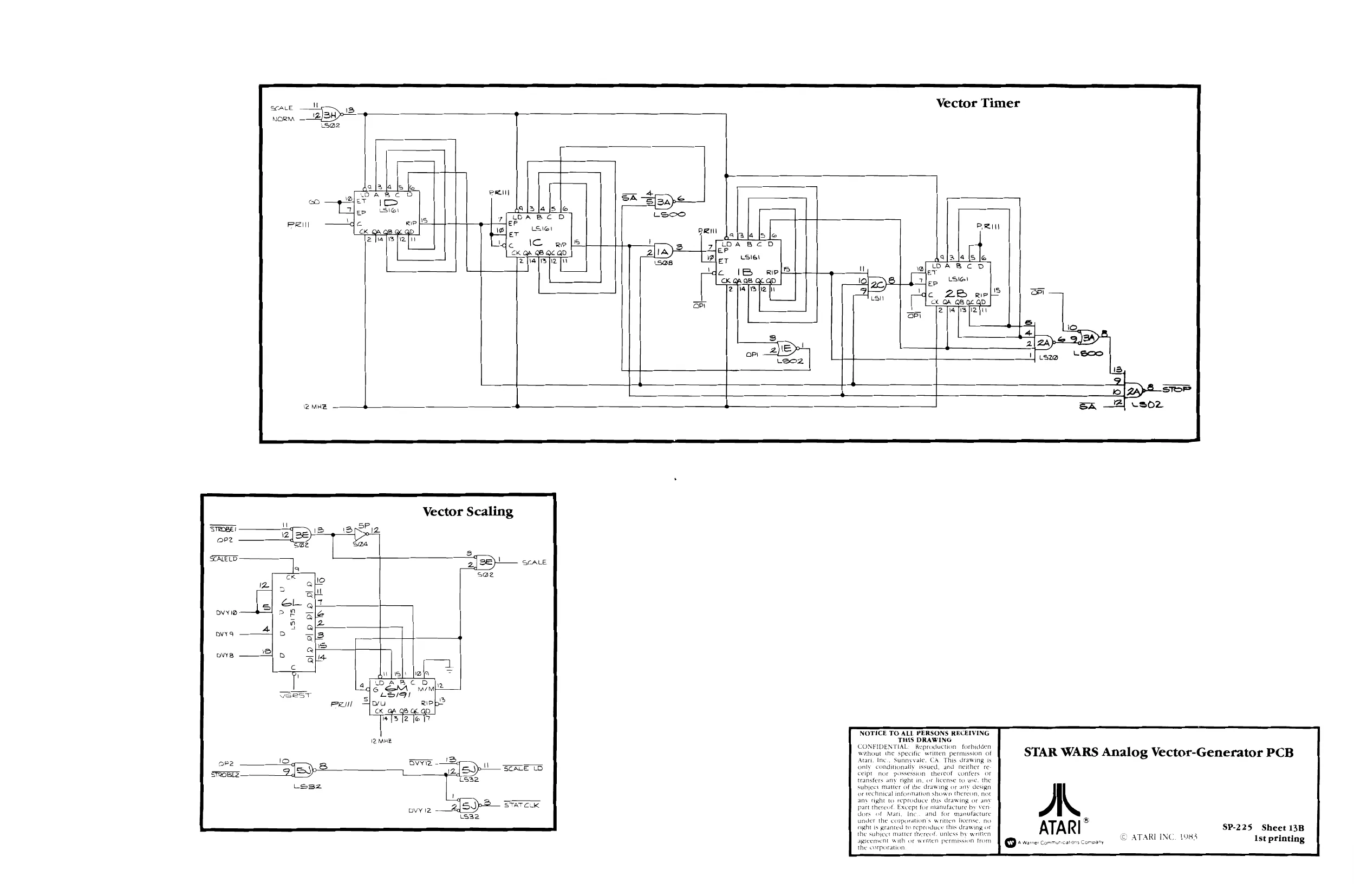
This page is a drawing, shown as the original scan.
+I5V
Ral
+I5V YCENTER : Res Te 150K
~BV _Byo
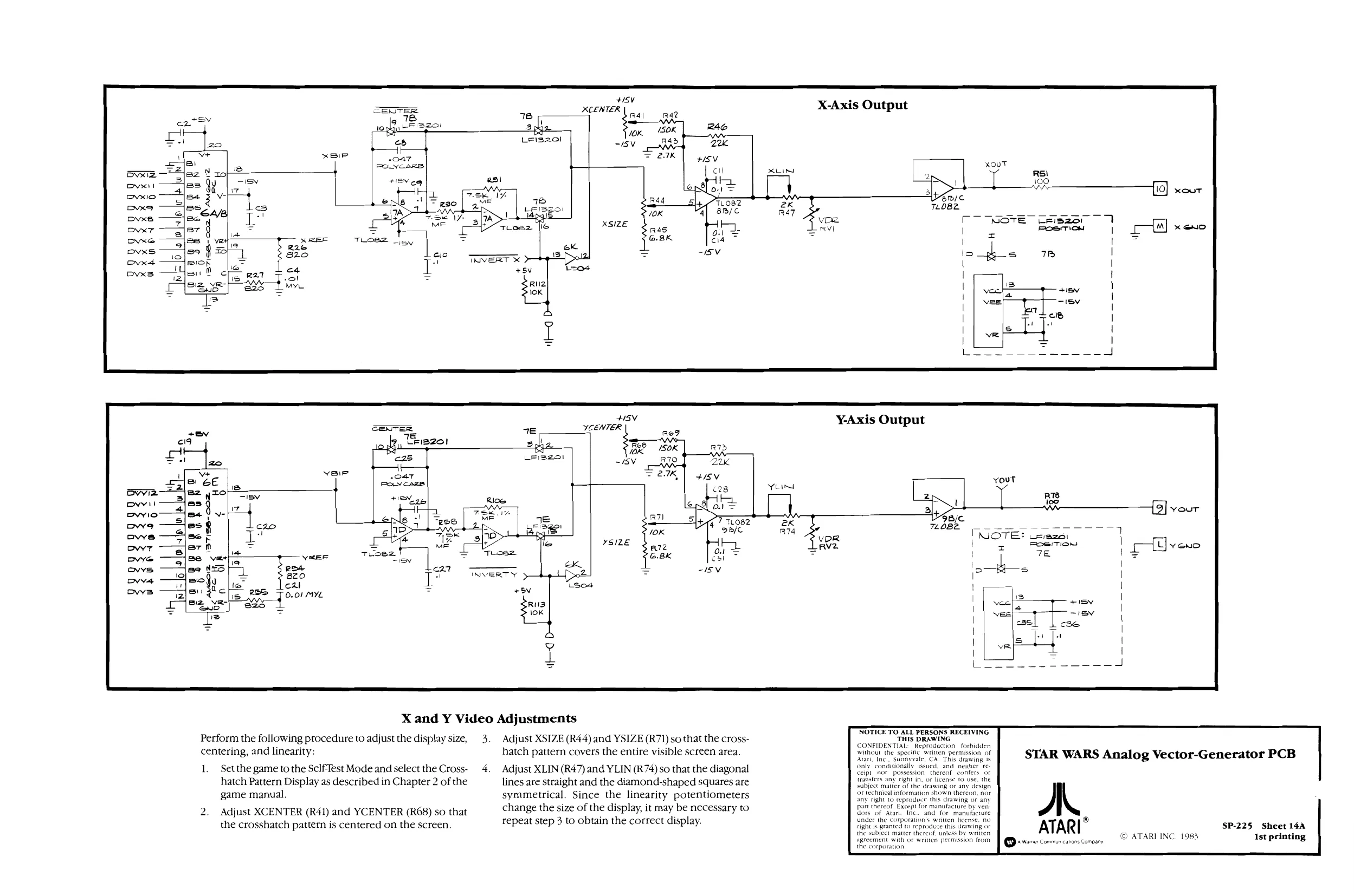
X-Axis Output
oe 3]
OTE LFiSz01 BOSTON
7B
E sev Ae TL og
X and Y Video Adjustments
Perform the following procedure to adjust the display size, centering, and linearity:
1, Set the game to the Self-Test Mode and select the Crosshatch Pattern Display as described in Chapter 2 of the game manual.
Adjust XCENTER (R41) and YCENTER (R68) so that the crosshatch pattern is centered on the screen. Adjust XSIZE (R44) and YSIZE (R71) so that the crosshatch pattern covers the entire visible screen area.
Adjust XLIN (R47) and YLIN (R74) so that the diagonal lines are straight and the diamond-shaped squares are symmetrical. Since the linearity potentiometers change the size of the display, it may be necessary to repeat step 3 to obtain the correct display. NOTICE TO ALL PERSONS RECEIVING THIS DRAWING CONFIDENTIAL: "Reproduction forbidden without the specific written permission of Atari, Inc.. Sunnyvale, CA. This drawing 1S only conditionally issued, and neither re ceipt Aor possession thereof confers oF tranafers any right in, or license (0 use, the subject matter of the drawing Or any design or technical information shown thereon, nor any right to ceproduce this drawing or any part thereof Except for manufacture by ven dors of Atari, Inc. and for manufacture Under the Corporation's written license, 0 fight 1s granted to reproduce this drawing or the subject matter thereof, unless by written agreement with or written permission from the corporation
STAR WARS Analog Vector-Generator PCB
© = v2r2:conmancarons company © ATARI INC. 1983, SP-225 Sheet 14A Ist printing
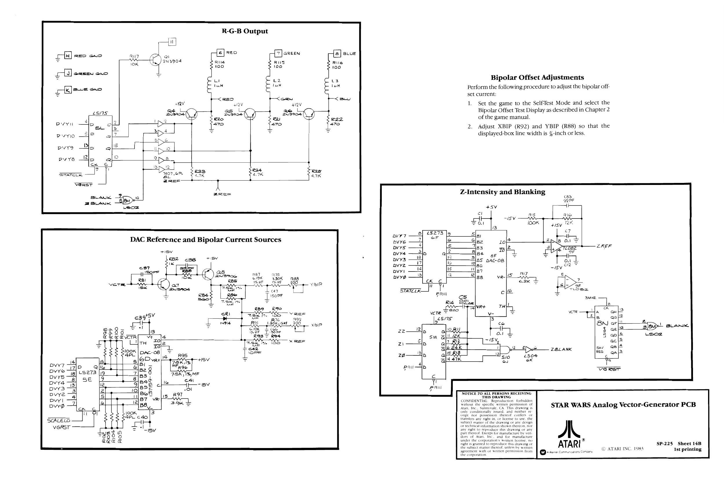
R-G-B Output
Qi 2Nd904
Bipolar Offset Adjustments
Perform the following procedure to adjust the bipolar offset Current:
- Set the game to the Self-Test Mode and select the Bipolar Offset Test Display as described in Chapter 2 of the game manual.
- Adjust XBIP (R92) and YBIP (R88) so that the displayed-box line width is 4-inch or less.
ovy7
DVYG Dvys pvy4 Dvy3 Dye
avy! pvyo
DAC Reference and Bipolar Current Sources
+iBV )
>
fe 14] Berk RIS
| ol | 130K | 8! | |
| Res | ‘eur | Neue | Re |
ae Me C47 [isonr cK in Fr 4— YRIP STATCLK—J PRI J os R46 BElee Lys a RBG RIO BZ0 VETR 15° Y REE “s/7s
| ne | 76 | Ree |
Rot ESE ue 256 loa
WK 7 Ri2 1
pee é ZBLANK [SEAR 14 47K eK te Gude J Soar R93 = RI4
FEL NES Ae Re: [ore Ss Aa f tv = x REF DID plo oO
Orso
PBI 1%) MF
NOTICE TO ATL PERSONS RECEIVING "THIS DRAWING CONADENTIAL Reproduction forbidden Rae ine. Ssermeeale Ch. The deaeing is STAR WARS Analog Vector-Generator PCB
subject matter OF the drawing or any design
br technical information shown thereon, nor any’ right to reproduce this drawing of any part thereof. Excepe for manufacture by ven: dors of Atari, Inc. and for manufacture . under the corporation's writen license. m0 ® ist ase teh Rng ATARI $P-225. Sticer'4e saecement with of written permission from QO rvererconmecarons conoany ATARI INC. 1983 Ist printing the corporation,
This page is a drawing, shown as the original scan.
This page is a drawing, shown as the original scan.
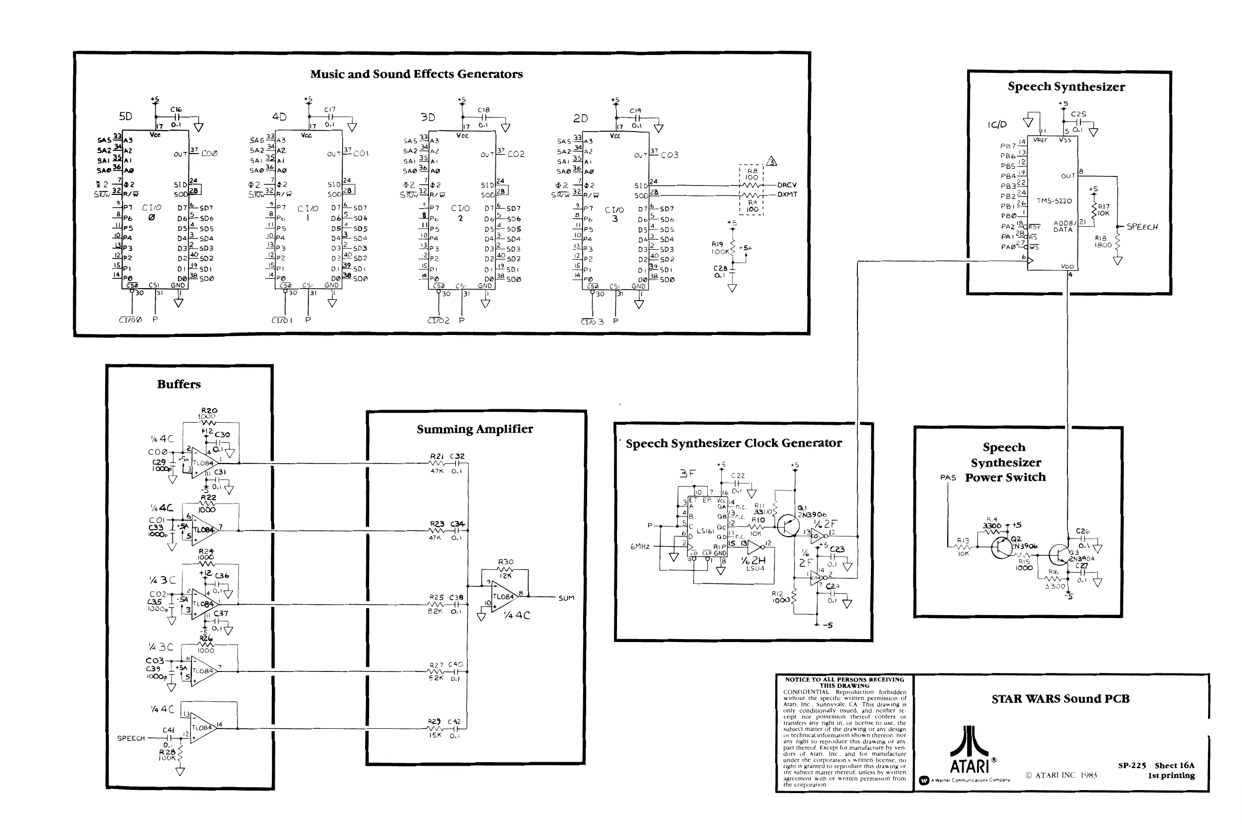
Music and Sound Effects Generators
+8 +5
cr 7 O-! b Vee.
BZ cor
es
Ip 3 Alpe
ps Po. eSB cs ia 31 C2 P
Summing Amplifier
R2i C32 Vt 47K 0.1
* Speech Synthesizer Clock Generator
Speech Synthesizer
+8
c2s io VI bard VReF
out
TMS-5220
roy | ADDB/ ROY DATA es
ws
lui, 1K NS a5 !2
%o2H (soa
NOTICE TO ALL PERSONS RECEIVING THIS DRAWING CONFIDENTIAL Reproduction forbidden, without the specific written permission of Atari, Inc., Sunnyvale, CA. This drawing is only conditionally issued, and. neither re: ceipt_nor possession thereof confers or transfers any right in, or license to use, the
subject matter of the drawing or any design
(or technical information shown thereon. Aor
any right to reproduce this drawing oF any part thercof. Except for manufacture by ven. dors of Atari, Inc, and for manufacture under the corporation written license, no right 1s granted to reproduce this drawing or the subject matter thereof, uniess by written agreement with oF Weitten permission from the corporation Speech Synthesizer Pas Power Switch
A ATARI © + 21267 Communcavons Comoany STAR WARS Sound PCB
®
© ATARI INC. 1983 SP-225 Shect 16A Ist printing
This page is a drawing, shown as the original scan.
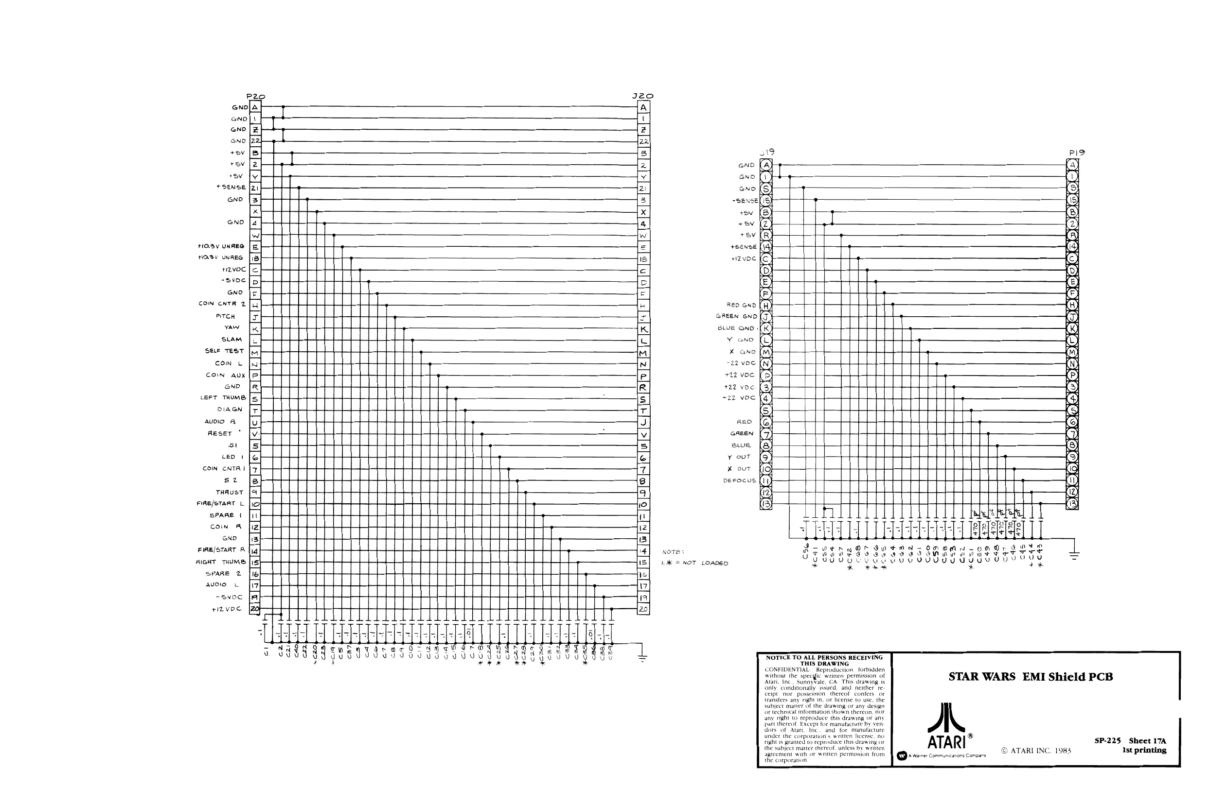
This page is a drawing, shown as the original scan.
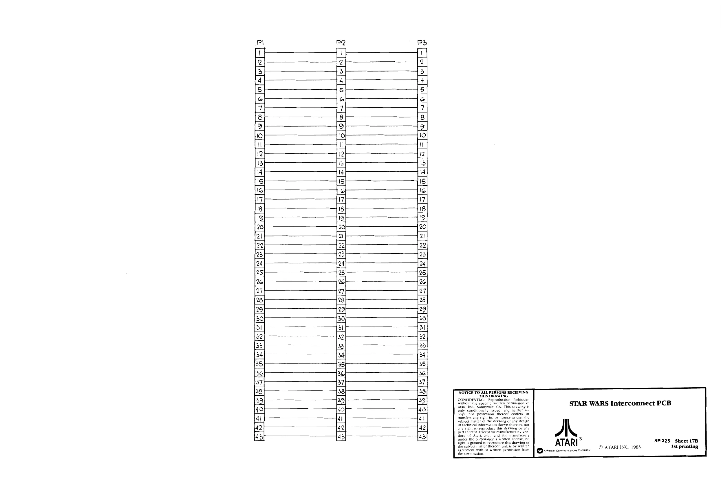
This page is a drawing, shown as the original scan.
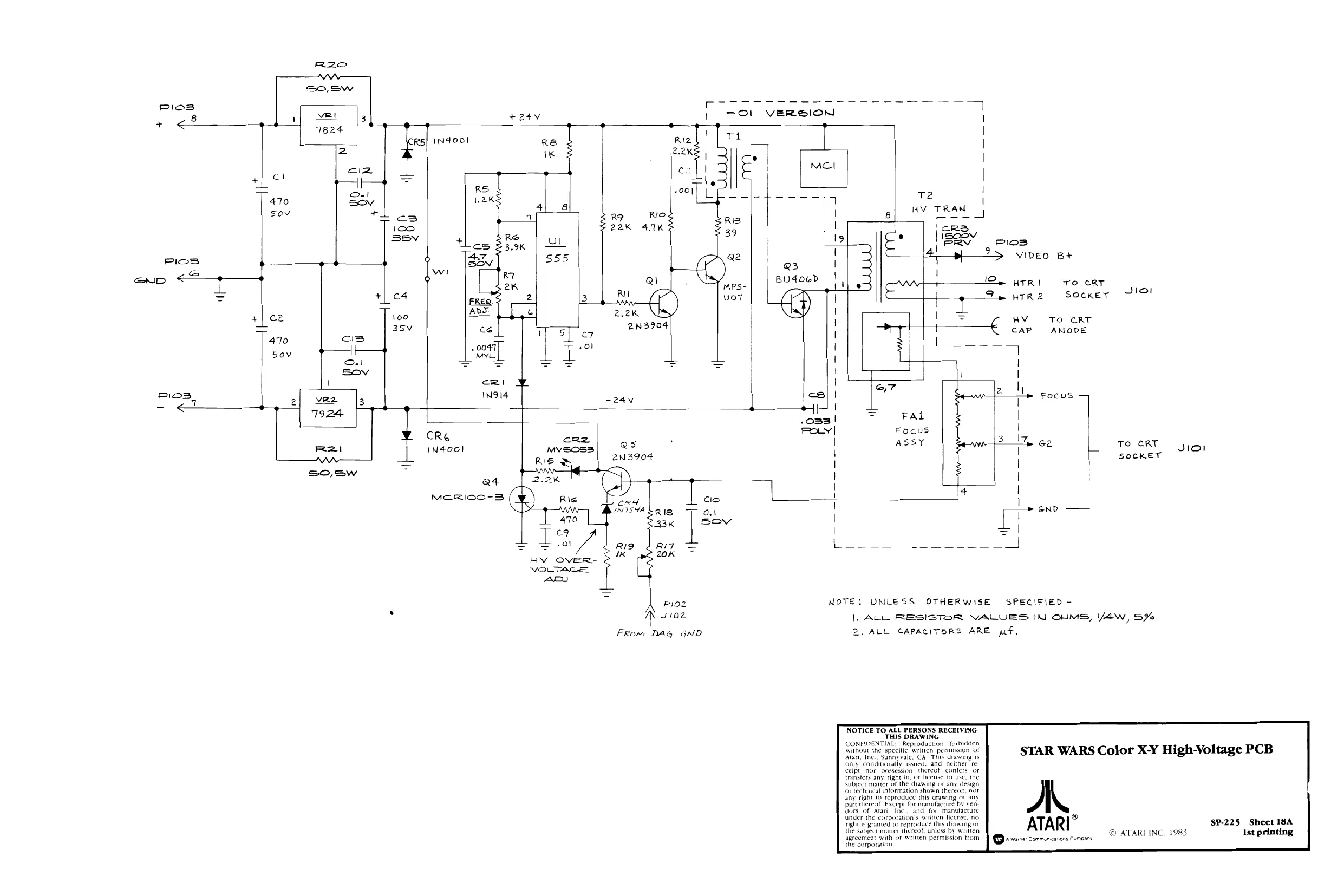
This page is a drawing, shown as the original scan.
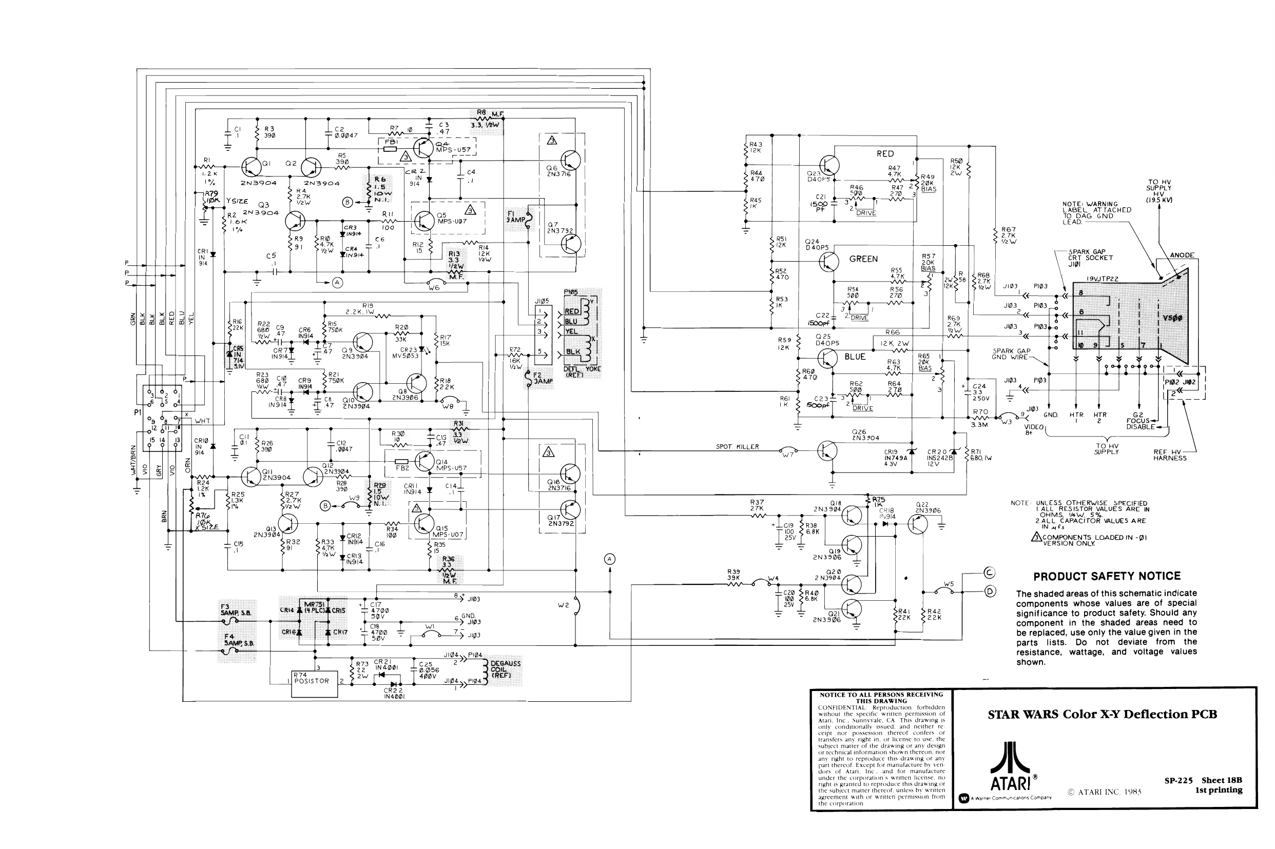
This page is a drawing, shown as the original scan.