Space Duel SP-181 2nd Printing
Space Duel (version 2) (Atari, 1980) · Schematic Package · 20 pages · 26 sections · original scan
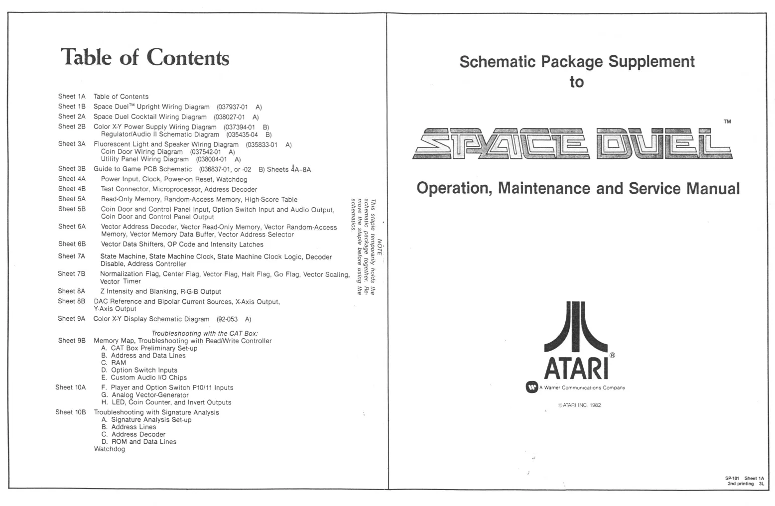
Table of Contents Schematic Package Supplement
to
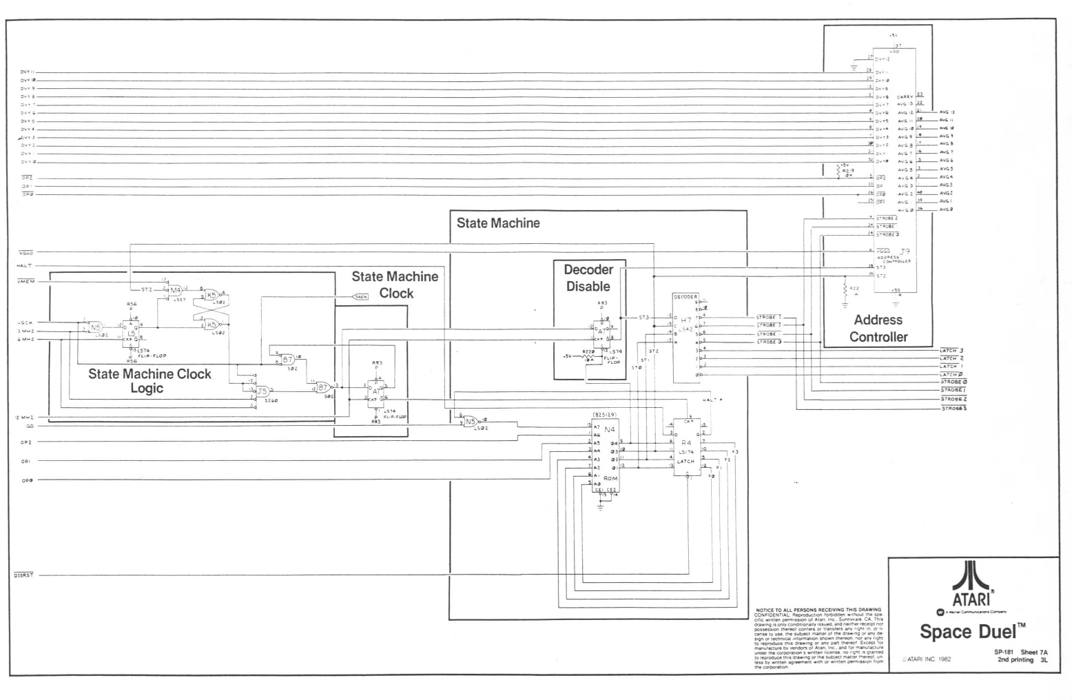
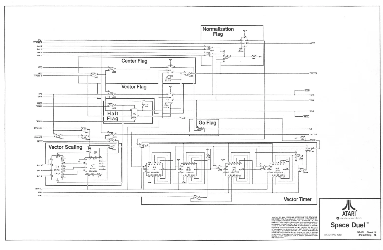
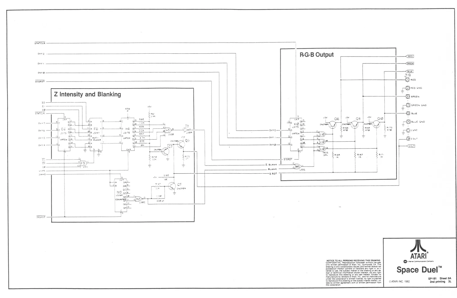
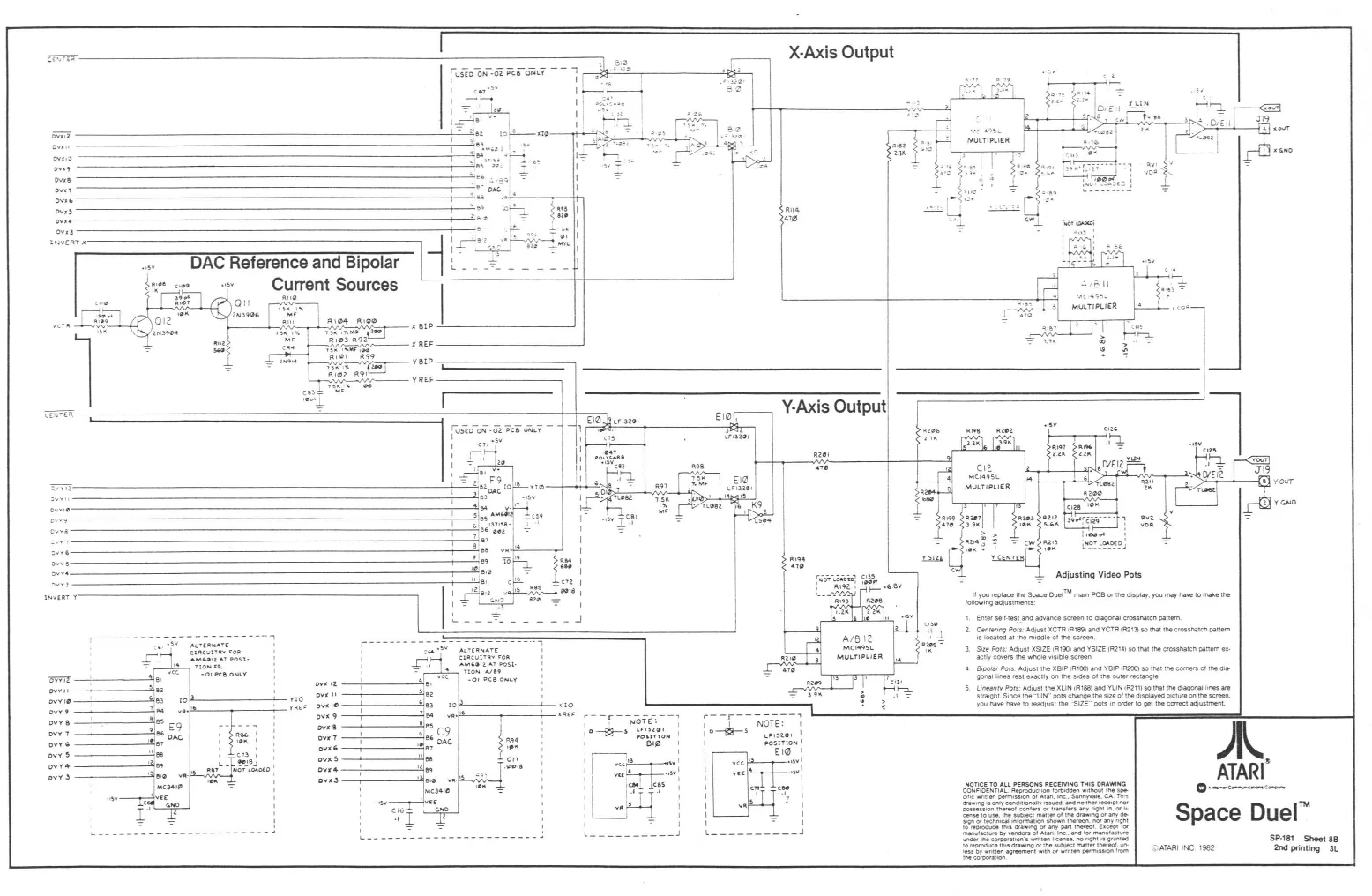
Sheet 1A Table of Contents Sheet 18 Space Duel™ Upright Wiring Diagram (03793701 A) Sheet 2A Space Duel Cocktail Wiring Diagram (038027-01 A) Sheet 28 Color XY Power Supply Wiring Diagram (037394-01 B) = 5 ia {12 al = RegulatoriAudio ll Schematic Diagram (03543504 8) na ay Sheet 3A Fluorescent Light and Speaker Wiring Diagram (036833-01 A) Ss i\\ NL] (l 7 Coin Door Wiring Diagram (03754201 A) Utility Panel Wiring Diagram (03800401 A) Sheet 38 Guide to Game PCB Schematic (036837-01, or 02 B) Sheets 4a-8A Sheet 4A Power Input, Clock, Power-on Reset, Watchdog . . . Sheet 48 Test Connector, Microprocessor, Address Decoder Operation, Maintenance and Service Manual Sheet 5A Read-Only Memory, Random-Access Memory, High-Score Table Sheet 5B Coin Door and Control Panel Input, Option Switch Input and Audio Output, Coin Door and Control Panel Output Sheet 6A Vector Address Decoder, Vector Read-Only Memory, Vector Random-Access Memory, Vector Memory Data Buffer, Vector Address Selector Sheet 6B Vector Data Shifters, OP Code and Intensity Latches Sheet 7A _ State Machine, State Machine Clock, State Machine Clock Logic, Decoder Disable, Address Controller Sheet 7B Normalization Flag, Center Flag, Vector Flag, Halt Flag, Go Flag, Vector Scaling, Vector Timer Sheet 8A —_Z Intensity and Blanking, R-G-B Output Sheet 8B DAC Reference and Bipolar Current Sources, X-Axis Output, Y-Axis Output Sheet 9A Color XY Display Schematic Diagram (92-053 A) sonpweyos ay) Buisn a10jaq o/ders oy) onow ‘24 say1960} abeyord oNewayos ay) spjoy Ayesodusay ajders sty
BON
Troubleshooting with the CAT Box: Sheet 98 Memory Map, Troubleshooting with ReadiWrite Controller A. CAT Box Preliminary Set-up B. Address and Data Lines Cc. RAM D. Option Switch Inputs E. Custom Audio 0 Chips Sheet 10A —_F. Player and Option Switch P10/11 Inputs > vere: conmuncatons Comoany G. Analog Vector-Generator H. LED, Coin Counter, and Invert Outputs ATARI INC. 1982 Sheet 10B Troubleshooting with Signature Analysis ‘A. Signature Analysis Set-up B. Address Lines C. Address Decoder D. ROM and Data Lines Watchdog
SPIO Sheet 18 ‘2nd panting 3
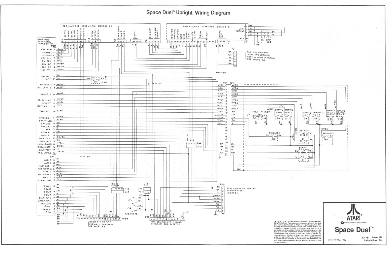
This page is a drawing, shown as the original scan.
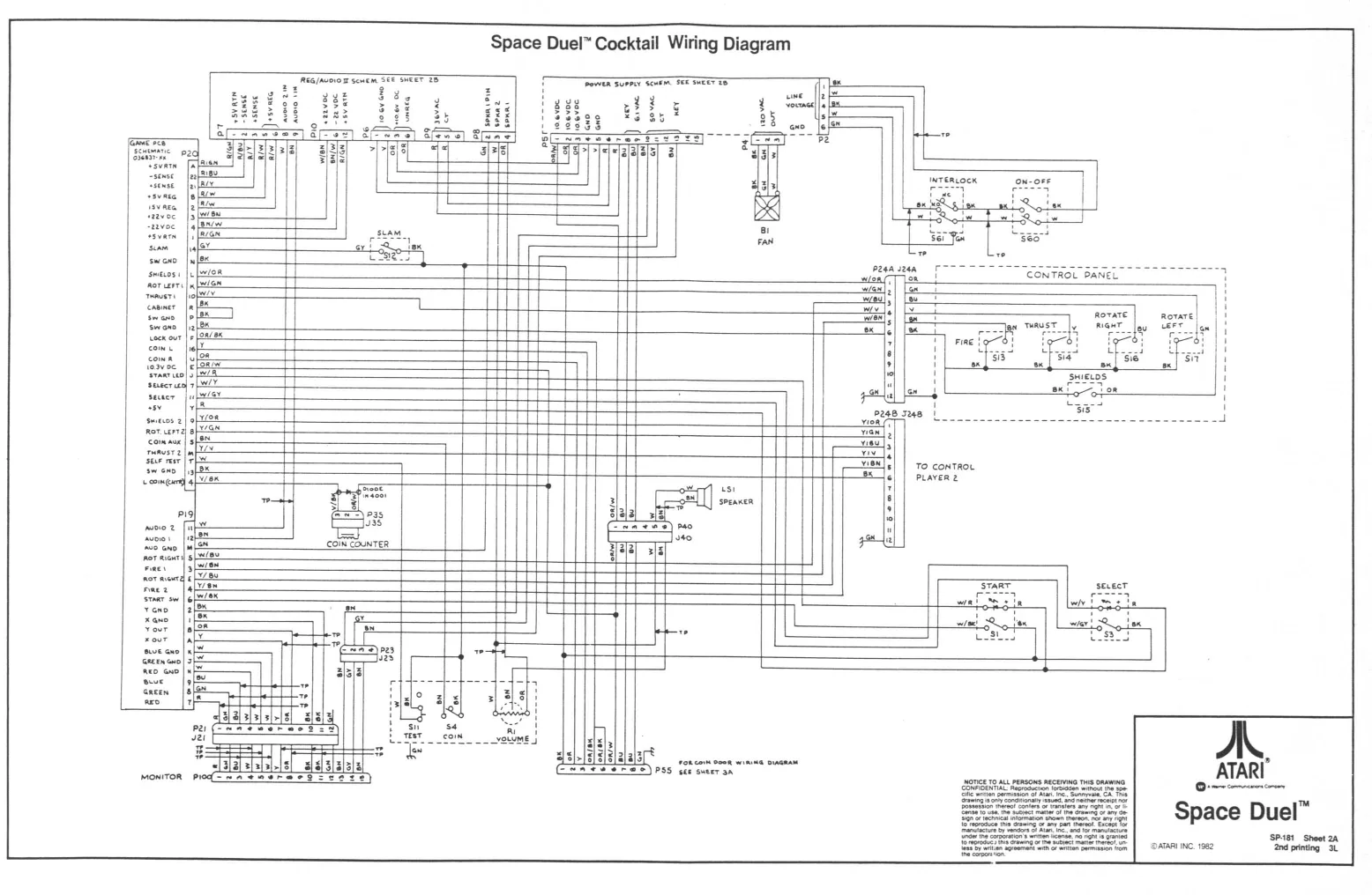
This page is a drawing, shown as the original scan.
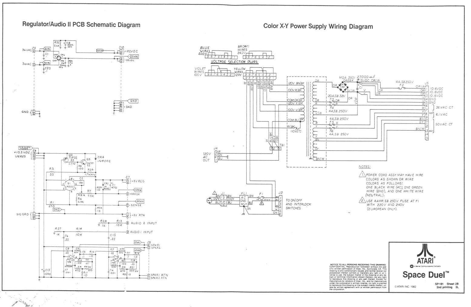
This page is a drawing, shown as the original scan.
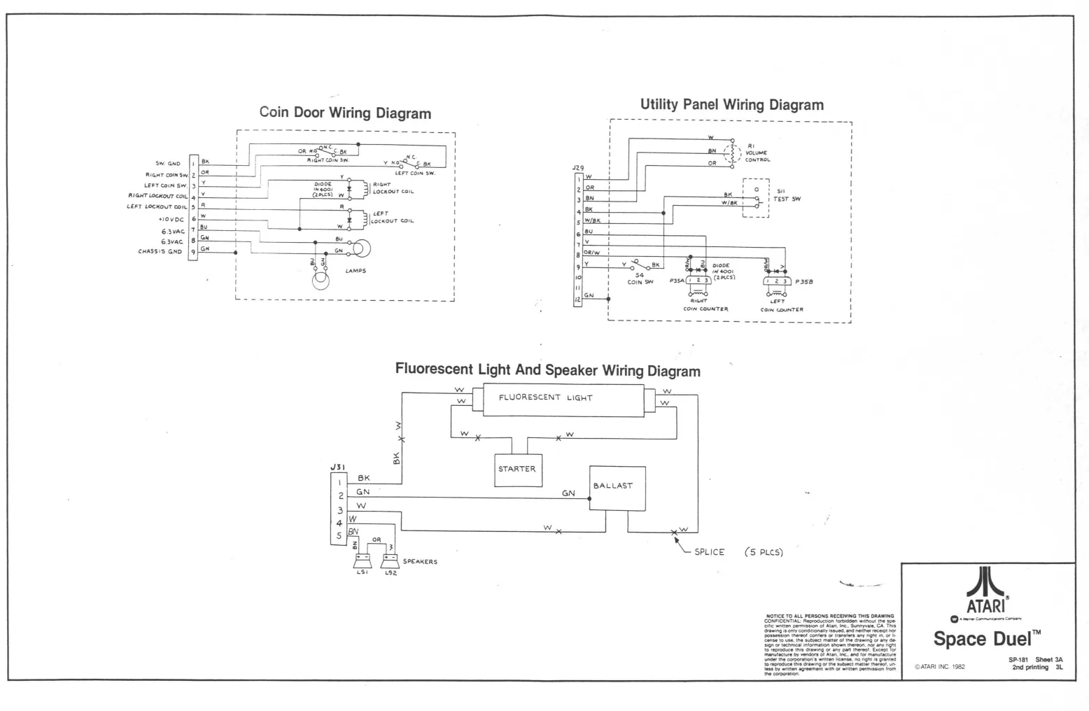
This page is a drawing, shown as the original scan.
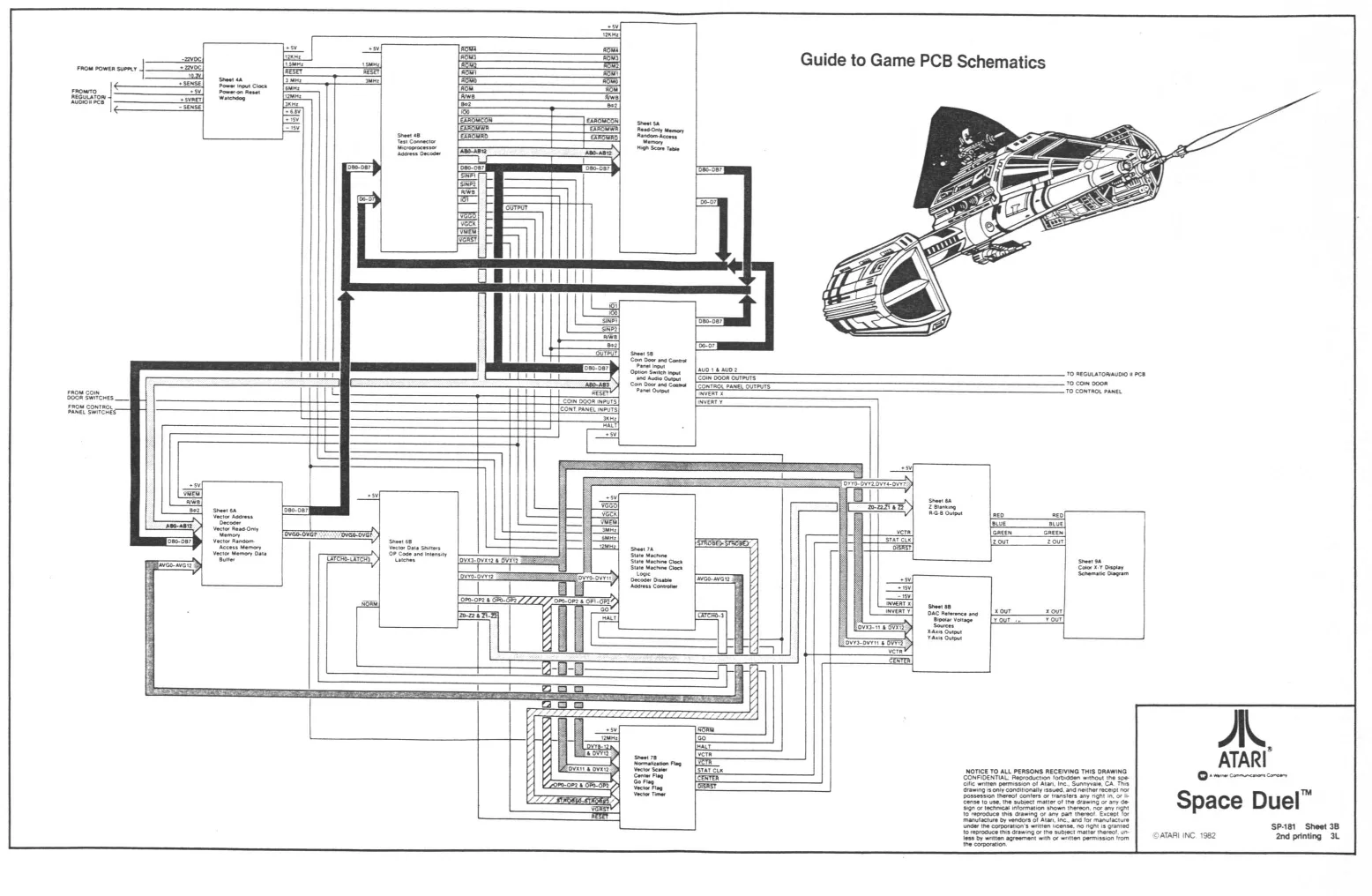
This page is a drawing, shown as the original scan.
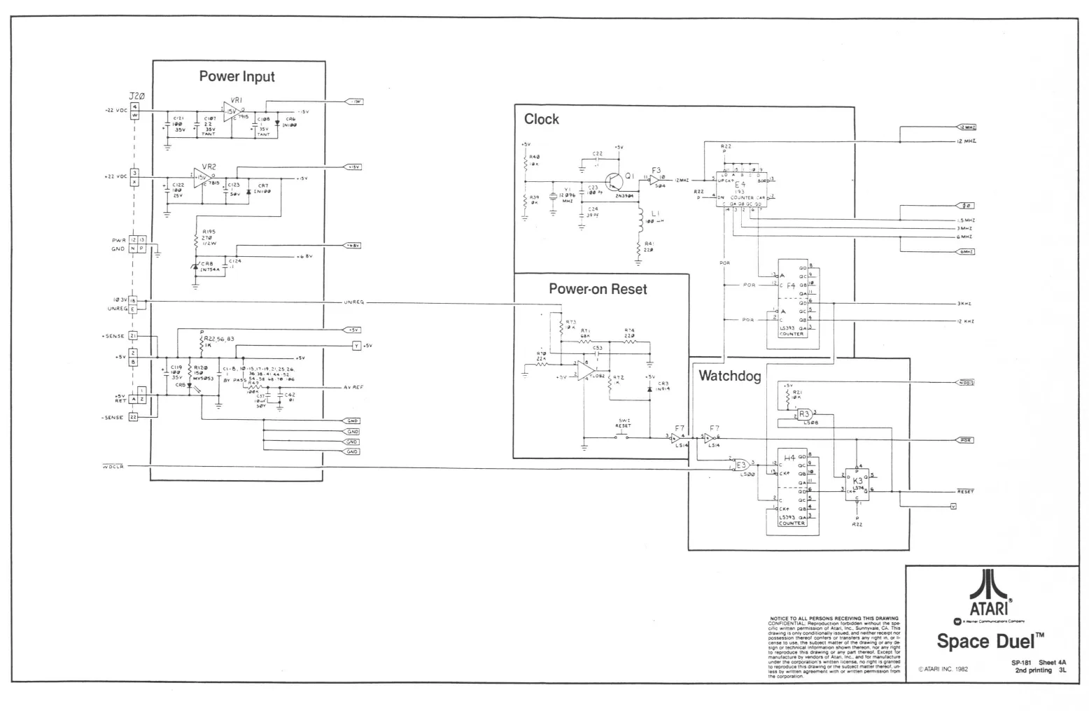
This page is a drawing, shown as the original scan.
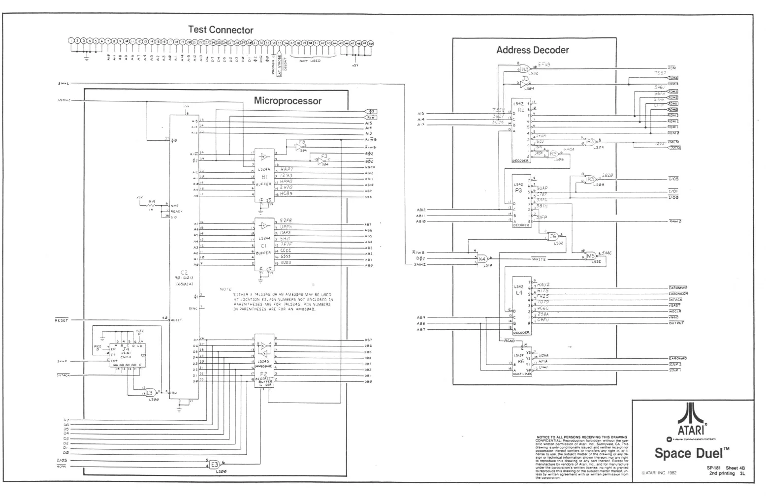
This page is a drawing, shown as the original scan.
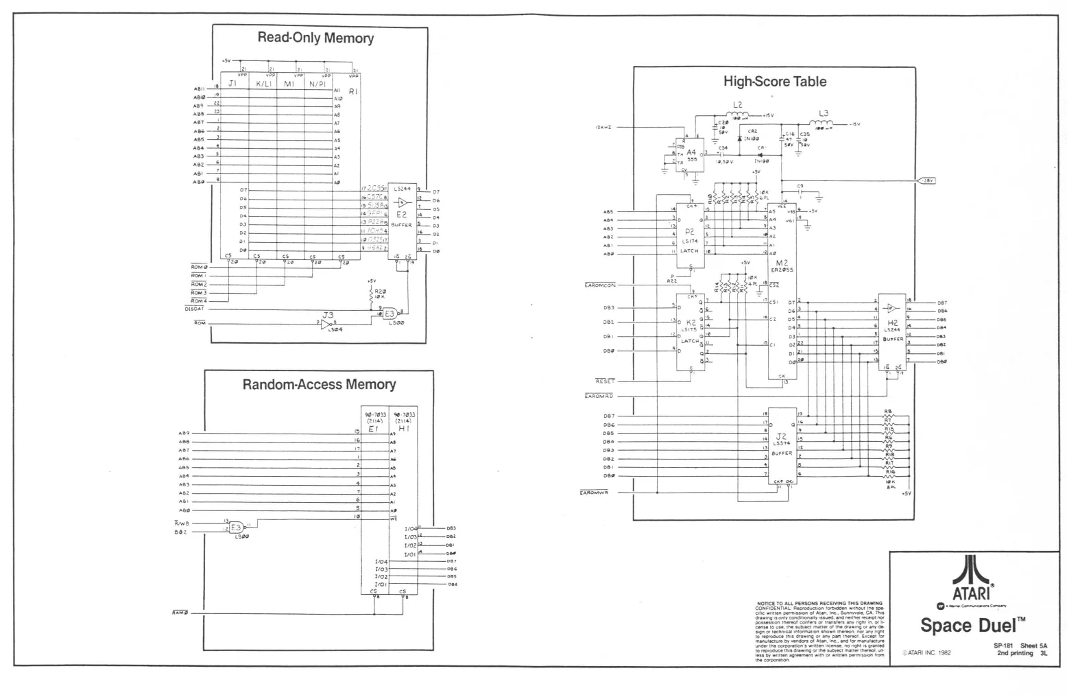
This page is a drawing, shown as the original scan.
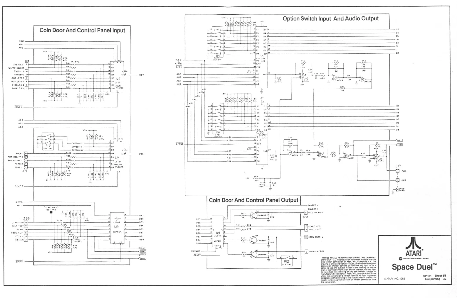
This page is a drawing, shown as the original scan.
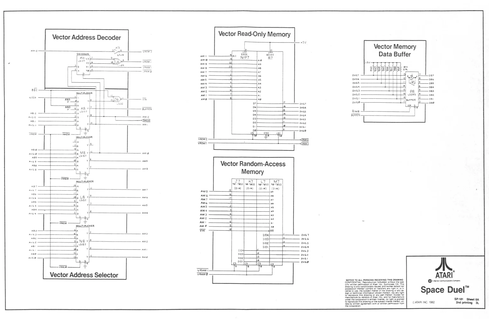
This page is a drawing, shown as the original scan.
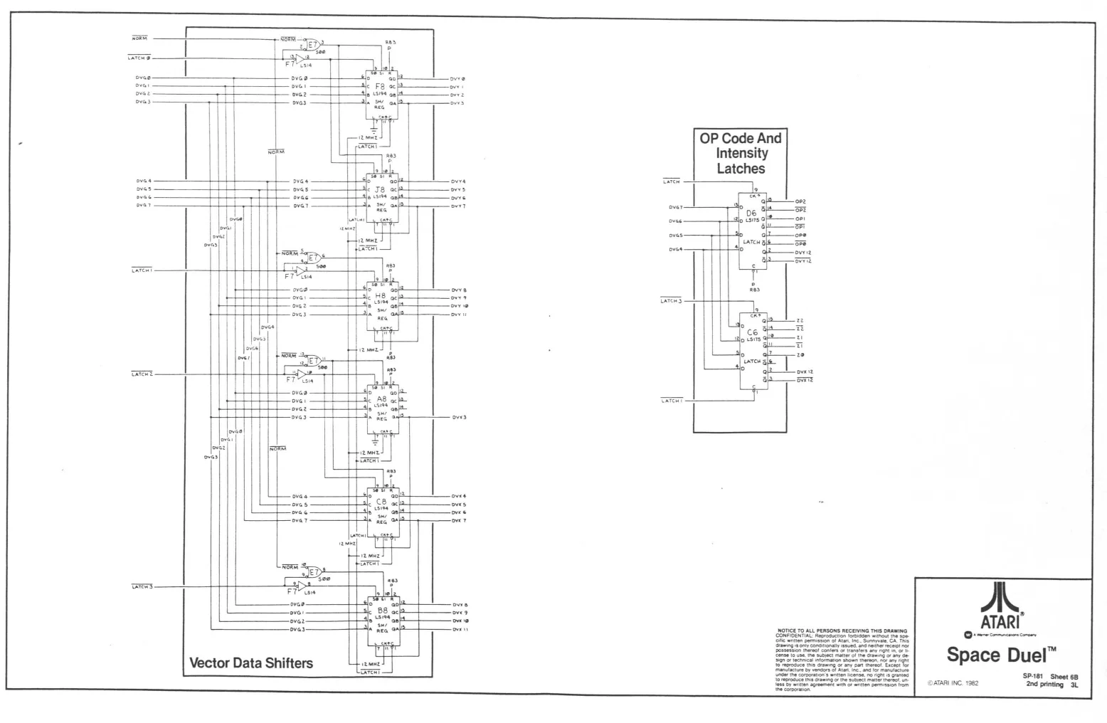
This page is a drawing, shown as the original scan.
This page is a drawing, shown as the original scan.
This page is a drawing, shown as the original scan.
This page is a drawing, shown as the original scan.
This page is a drawing, shown as the original scan.
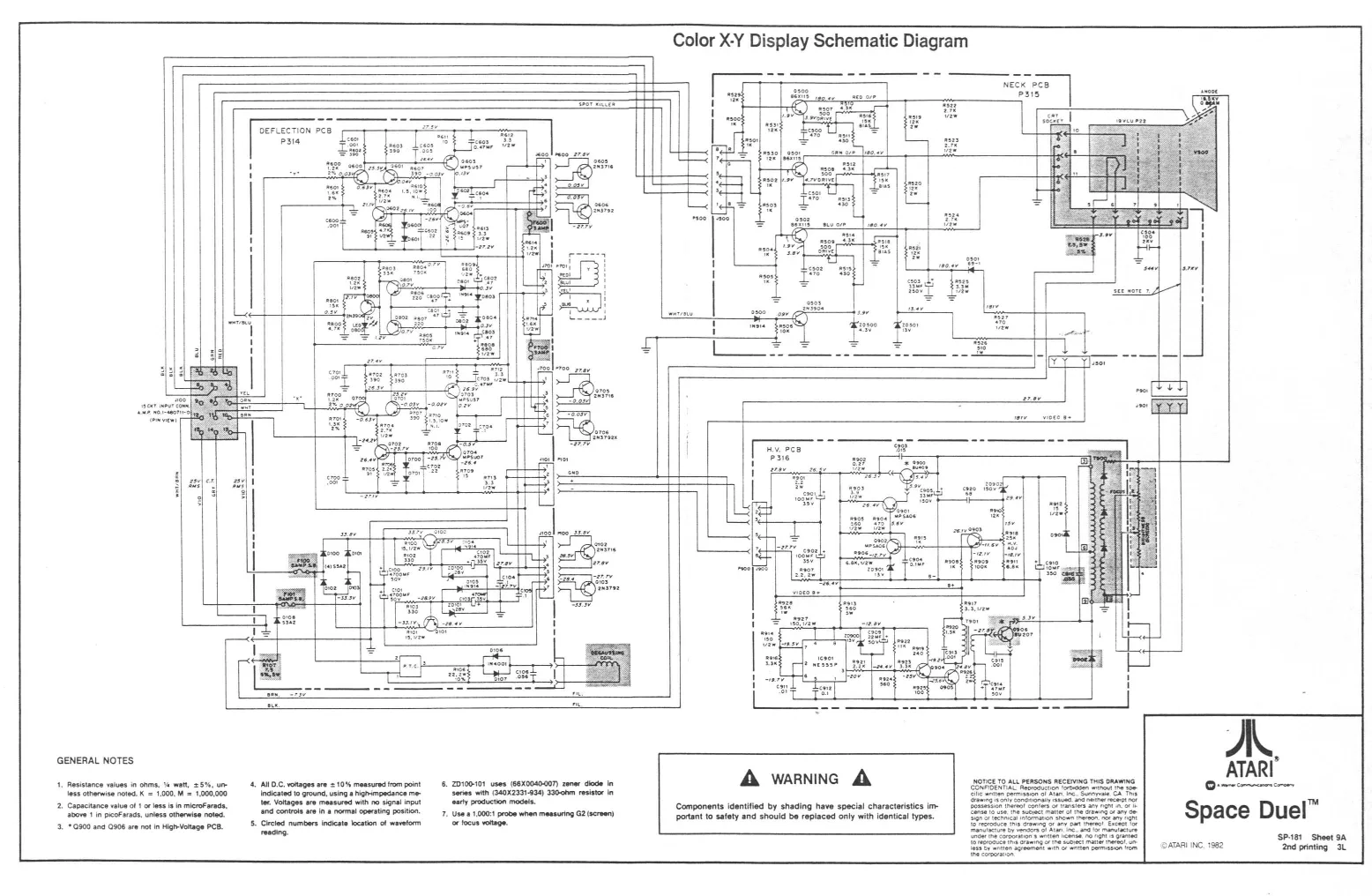
This page is a drawing, shown as the original scan.
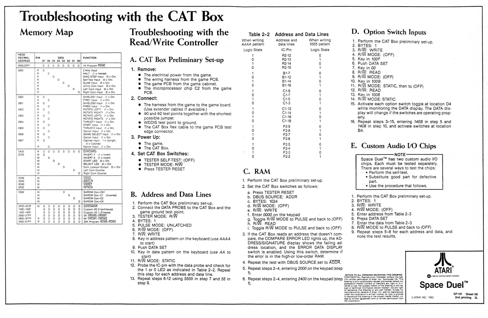
This page is a drawing, shown as the original scan.
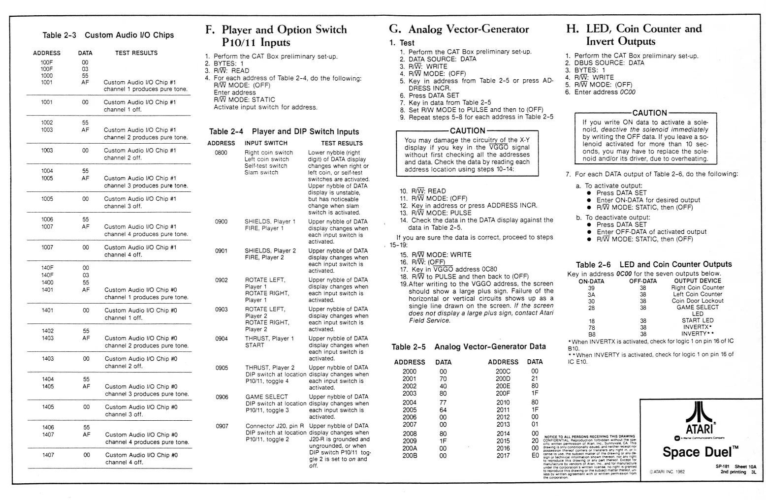
Table 2-3 Custom Audio I/O Chips
ADDRESS DATA TEST RESULTS 100F 00 s00F 03 1000 55
| 1001 | AF | Custom Audio /O Chip #1 |
channel 1 produces pure tone,
| 1001 | 00 | Custom Audio VO Chip #1 |
channel 1 off. 1002 55
1003 AF Custom Audio iO Chip #1
channel 2 produces pure tone.
| 1003, | 00 | Custom Audio VO Chip #1 |
channel 2 off. 1004 55
| 1008 | AF | Custom Audio 110 Chip #1 |
channel 3 produces pure tone.
| 1008 | 00 | Custom Audio VO Chip #1 |
channel 3 off
1008 55
| 1007 | AF | Custom Audio /]0 Chip #1 |
channel 4 produces pure tone.
| 1007 | 00 | Custom Audio VO Chip #1 |
channel 4 off. 140F 00 140F 03 +400 55
| 1401 | AF | Custom Audio 110 Chip #0 |
channel 1 produces pure tone.
| 1401 | 00 | Custom Audio WO Chip 40 |
channel 1 off.
s402 55
| 1403 | AF | Custom Audio 0 Chip #0 |
channel 2 produces pure tone.
| 1403 | 00 | Custom Audio VO Chip #0 |
channel 2 off. 1408 55
1405 AF Custom Audio iO Chip #0
channel 3 produces pure tone.
| 1405 | 00 | Custom Audio VO Chip #0 |
1408 55
| 1407 | AF | Custom Audio /]O Chip #0 |
channel 4 produces pure tone.
| 1407 | 00 | Custom Audio VO Chip #0 |
channel 4 off.
F. Player and Option Switch
P10/11 Inputs
BYTES: 1 RW: READ |. For each address of Table 2-4, do the following: RAW MODE: (OFF)
Enter addi
ress RAW MODE: STATIC Activate input switch for address,
Table 2-4
ADDRESS.
0800
0902
0904
0905 Perform the CAT Box preliminary setup.
Player and DIP Switch Inputs
INPUT SWITCH
Right coin switch Left coin switch Seif-test switen Slam switch
SHIELDS, Player 1 FIRE, Player 1
SHIELDS, Player 2 FIRE, Player 2
ROTATE LEFT, Player 1 ROTATE RIGHT, Player 1 ROTATE LEFT, Player 2 ROTATE RIGHT, Player 2 THRUST, Player 1 START
THRUST, Player 2 DIP switch at location Pr0it, toggle 4
GAME SELECT DIP switch at location P10/11, toggle 3
Connector J20, pin R DIP switch at location PI0/11, toggle 2 TEST RESULTS Lower nybble (right Gigit) of DATA display changes when right or left coin, or self-test switches are activated. Upper nybble of DATA display is unstable, but has noticeable change when siam switch is activated Upper nybble of DATA display changes when each input switch is activated.
Upper nybble of DATA display changes when each input switch is activated.
Upper nybble of DATA isplay changes when each input switch is, activated. Upper nybble of DATA display changes when each input switch is activated.
Upper nybble of DATA display changes when each input switch is activated. Upper nybble of DATA Gisplay changes when each input switch is activated. Upper nybbie of DATA display changes when ‘each input switch is activated, Upper nybbie of DATA display changes when 420 is grounded and ungrounded, or when DIP switch P1011 tog: gle 2 is set toon and ott G. Analog Vector-Generator
- Test Perform the CAT Box preliminary set-up. DATA SOURCE: DATA RAW: WRITE RW MODE: (OFF) Key in address from Table 2-5 or press AD- DRESS INCR. Press DATA SET Key in data from Table 2-5 Set RIW MODE to PULSE and then to (OFF) Repeat steps 5-8 for each address in Table 2-5
- RIW: READ
- RIW MODE: (OFF)
- Key in address or press ADDRESS INCR.
- RW MODE: PULSE
- Check the data in the DATA display against the data in Table 2-5.
If you are sure the data is correct, proceed to steps 18-19)
- RAW MODE: WRITE
- RAW: (OFF)
- Key in VGGO address 0C80
- RIW to PULSE and then back to (OFF) 49.After writing to the VGGO address, the screen should show a large plus sign. Failure of the horizontal or vertical circuits shows up as a single line drawn on the screen. /f the screen does not display a large plus sign, contact Atari Field Service.
Table 2-5 Analog Vector-Generator Data
| ADDRESS | DATA | ADDRESS | DATA |
| 2000 | 00 | 200C | 00 |
| 2001 | 70 | 2000 | 24 |
| 2002 | 40 | 200E | 80 |
| 2003 | 80 | 200F | 1F |
| 2004 | 7 | 2010 | 80 |
| 2005 | 64 | 2011 | la |
| 2006 | 00 | 2012 | 00 |
| 2007 | 00 | 2013 | 0 |
| 2008 | 80 | 2014 | |
| 2003 | 1 | 2015 | |
| 2008 | 00 | 2016 | |
| 2008 | 00 | 2017 |
H. LED, Coin Counter and Invert Outputs
Perform the CAT Box preliminary set-up. DBUS SOURCE: DATA BYTES: 1 RW: WRITE RIW MODE: (OFF) Enter address 0CO0 Perens
‘CAUTION If you write ON data to activate a solenoid, deactive the solenoid immediately by writing the OFF data. If you leave a solenoid activated for more than 10 seconds, you may have to replace the solenoid andlor its driver, due to overheating.
- For each DATA output of Table 2-6, do the following:
a. To activate output: © Press DATA SET @ Enter ON-DATA for desired output © FUW MODE: STATIC, then (OFF)
b. To deactivate output: © Press DATA SET © Enter OFF-DATA of activated output © RIW MODE: STATIC, then (OFF)
Table 2-6 LED and Coin Counter Outputs Key in address 0C00 for the seven outputs below. ‘ON-DATA OFF-DATA OUTPUT DEVICE
| 39 | 38 | Right Coin Counter |
| 3A | 38 | Left Coin Counter |
| 30 | 3 | Coin Door Lockout |
| 28 | 38 | GAME SELECT |
LED
| 18 | 8 | START LED |
| 7B | 38 | INVERTX* |
| 88 | 38 | INVERTY** |
= When INVERTX is activated, check for logic 1 on pin 16 of IC 810, = *When INVERTY is activated, check for logic 1 on pin 16 of Ic E10.
‘SP.81_ sheet 108, AAEL NG, 1982 ‘and printing 3k
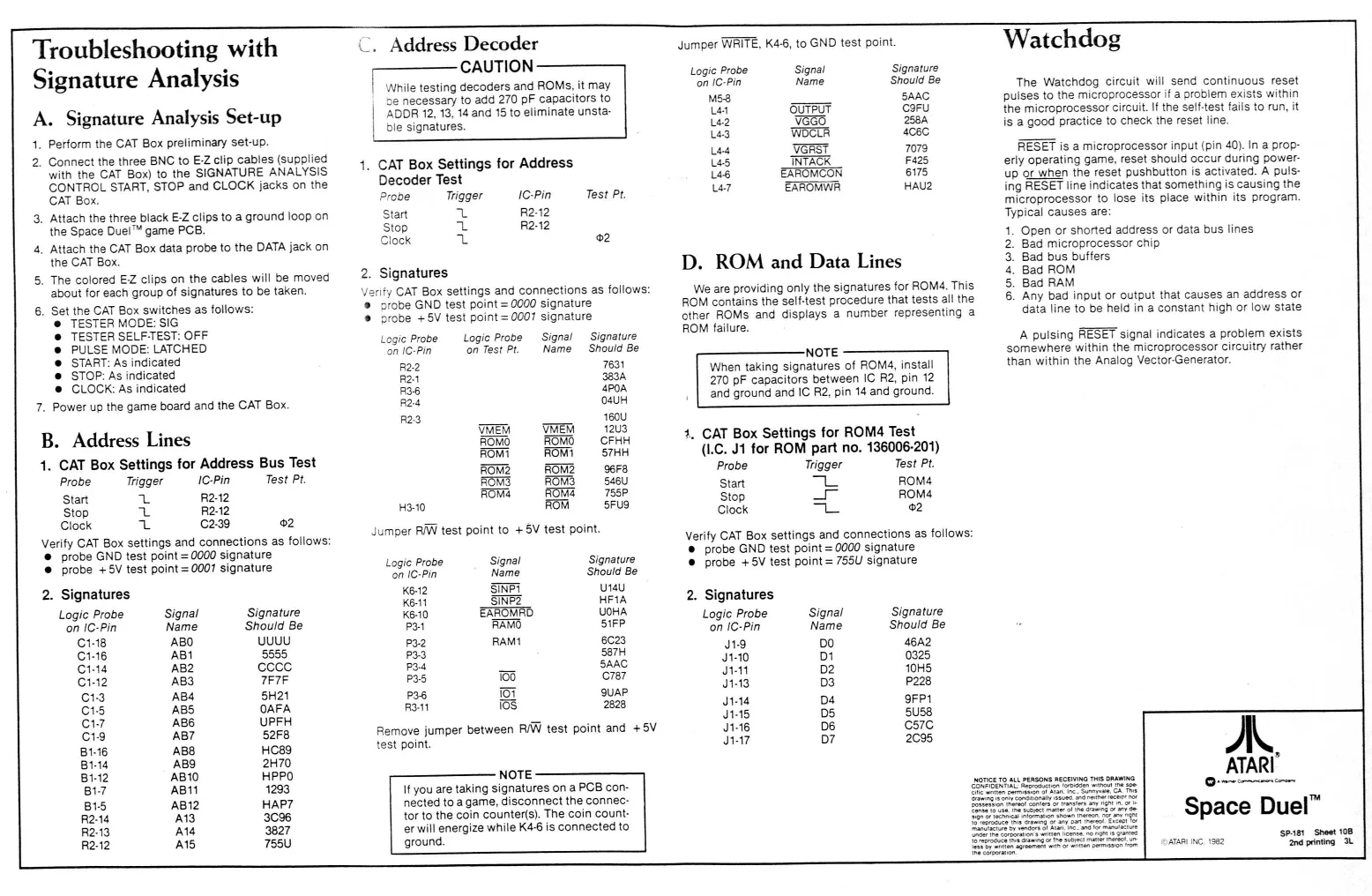
| Troubleshooting with | . | Address Decoder | Jumper WRITE, K46, to GND test point. | Watchdog | ||||
| . | ‘ | -— | CAUTION | Logie | Probe | si | ||
| ic Pr | Signal | Signature | ||||||
| Signature Analysis | eee | ae | a | scree | Sgn | Sey | cd comoue ut | |
| . | . | be necessary to add 270 pF capacitors to | Ms3 | SAAC | pulses to the microprocessor if a problem exists within | |||
| A. | Signature Analysis Set-up | | | ADDR 12, 13, 14 and 15 to eliminate unsta- | aa | oureut | coFU | the microprocessor circuit. If the self-test fails to run, it | |
| ble signatures. | tae | WGGO. | 250A | is a good practice to check the reset line. | ||||
| 1. | Perform the CAT Box preliminary set-up. | ree} | WOCTA | acec | ||||
| 2. Connect the three BNC to EZ clip cables (supplied | " | Les | VGRST | 7079 | AESET is a microprocessor input (pin 40). In a prop- | |||
| Connect the three BNC tO | eee | argsig | 1 | CAT Box Settings for Address | tas. | INTACK | F425 | erly operating game, reset should occur during power- |
| CONTROL START, STOP and CLOCK jacks on the | Decoder Test | L466 | FAROMCON | 6175 | up of when the reset pushbutton is activated. A puls- | |||
| CAT Box. | Probe | ‘Trigger | ~«=«sIGPin.~—‘Test Pt | Lar | EAROMWR | HaU2 | ing RESET line indicates that something is causing the | |
| a, Attach the tee black EZelips toa groundlcopon | Stat | = | RRM | mroprocesor fo lose is place witun is progam. | ||||
| the Space Duel™ game PCB. | Stop | a | R212 | |||||
| Clock | 1 | 02 | 4. Open or shorted address or data bus lines |
4, Attach the CAT Box data probe to the DATA jack on the CAT Box,
- The colored EZ clips on the cables will be moved about for each group of signatures to be taken.
- Set the CAT Box switches as follows: TESTER MODE: SIG TESTER SELF-TEST: OFF PULSE MODE: LATCHED START: As indicated STOP: As indicated CLOCK: As indicated
- Power up the game board and the CAT Box.
B. Address Lines
- CAT Box Settings for Address Bus Test
| Probe | Trigger | IC-Pin | Test Pt. |
Start L R212
Stop % R212
| Clock | L | 2.39 | 02 |
Verity CAT Box settings and connections as follows:
© probe GND test point = 0000 signature
- Signatures fy CAT Box settings and connections as follows: ‘® probe GND test point = 0000 signature
© probe +5V test point = 0007 signature
| Logic Probe | Logic Probe | Signal | Signature |
| on IC-Pin | on Test Pt. | Name | Should Be |
R22 7631 Rot 383A 36 4POA FO4 OaUH R23 1600 HEM 1203 ROMO © CFHH ROMi —S7HH FOND = 96F8 ROMS = 5460 oma = 756P
| +H3-10 | ROM | SFUS |
Jumper RIW test point to + SV test point. D. ROM and Data Lines
We are providing only the signatures for ROMA. This ROM contains the self-test procedure that tests all the other ROMs and displays a number representing a ROM failure.
- CAT Box Settings for ROM4 Test (ILC. J1 for ROM part no. 136006-201)
| Probe | Trigger | Test Pt. |
| Start | mk | ROMs |
| Stop | a | ROM |
| Clock | ~The | 2 |
Verify CAT Box settings and connections as follows:
Bad microprocessor chip Bad bus buffers Bad ROM Bad RAM Any bad input or output that causes an address or data line to be held in a constant high or low state Perey
A pulsing AESET signal indicates a problem exists somewhere within the microprocessor circuitry rather than within the Analog Vector-Generator.
| © probe +5V test point = 0001 signature | bogie cae | ional | Phd | © probe +5V test point = 755U signature |
| 2. Signatures | Ke12 | SNP | urau |
be ic Probe Signal Signature kon oe HFIA 2. Signatures
| i | fur | 6-10 | FA | OHA | ||||
| (on IC-Pin | Name | Should Be | ee | FAW | StFP | thee | = it | foe |
| 118 | ABO | uuuu | Poe | RAMI | 8c23 | |||
| C116 | ABI | 5555 | P33 | Sern | w19 | Do | 46A2 | |
| C114 | AB2 | ccc | P34 | _ | SAAC | 31-10. | Al | 0325 |
| C112 | ABS | FTF | P35 | 105 | C787 | a1 | b2 | ws |
| C13 | AB4 | 5H21 | P36 | Ford | 9uAP | roiled | Le | bed |
| C15 | ABS | OAFA | Raat | ios | 2828 | Jit4 | D4 | oFPt |
| c17 | ABE | UPFH | — | - | J145 | DS | 5US8 | |
| C13 | ‘AB7 | 52F8 | Remove jumper between RW test point and +5V | J416 | 06 | cs7c | ||
| Bit6 | ‘ABB | C89 | test point, | Jai | D7 | 2095 | ||
| B11 | ABO | 2H70 | ||||||
| Brie | B10 | HPPO | NOTE | ATARI | ||||
| B17 | ABit | 1293 | If you are taking signatures on a PCB con- | ones ro su gensows pesmne nes aang | i |
AB12 HAP7 nected to agame, disconnect the connec: ™
| ANS | 3096 | tor to the coin counter(s). The coin count- | Space Duel |
| Ala | 3827 | er will energize while K4-6 is connected to | |
| ANS | 755U | ground. | P81 Sheet 108 |
ATARI INC, 1862 “and peinting 3b