Karate Champ Installation Instructions
Karate Champ (US) (Data East USA, 1984) · Installation · 44 pages · 21 sections · original scan
KARATE CHAMP
PLAYER vs PLAYER
INSTALLATION INSTRUCTIONS
WARNING
This equipment generates and uses radio frequency energy and if not installed and used properly, i.e., in strict accordance with the instructions manual, may cause harmful interference to radio communications. It has been tested and found to comply with the limits for a Class A computing device persuant to Subpart J of Part 15 of FCC Rules, which are designed to provide reasonable protection against such interference when operated in a commercial environment.
Operation of this equipment in a residential area is likely to cause interference in which case the user at his own expense will be required to take whatever measures may be required to correct the interference.
EMI Shield must be securely installed in order to protect against undesirable radio interference.
KARATE CHAMP ™
Player Vs Player
TABLE OF CONTENTS
PAGE 1 Game Instructions
2 Joystick movements 3 Option Switch Settings 4 Major cabinet component locations
5 Power Supply Requirements Operating Environment Raster Scan Monitor Requirements 6 Main Harness PCB Terminations
7 Coin Counter Circuit 8 Sanken SWS 60 B Power Supply
9 KAGA KGD23S MK II Power Supply 12 Power Supply Circuit - Wells Gardner monitor games 13 Power Supply Circuit - NANAO or SANWA monitor games
1h Schematic diagram - Wells Gardner monitor
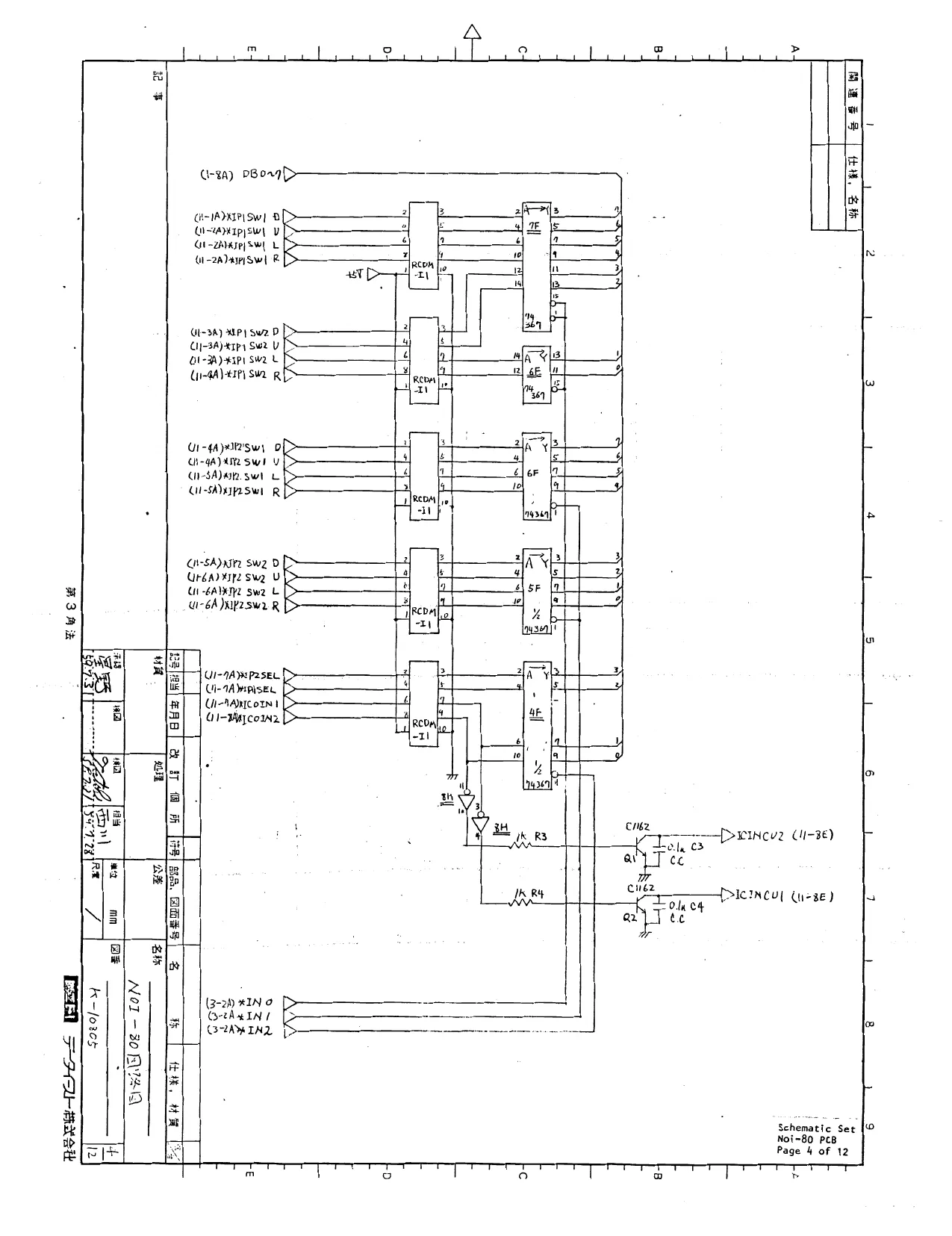
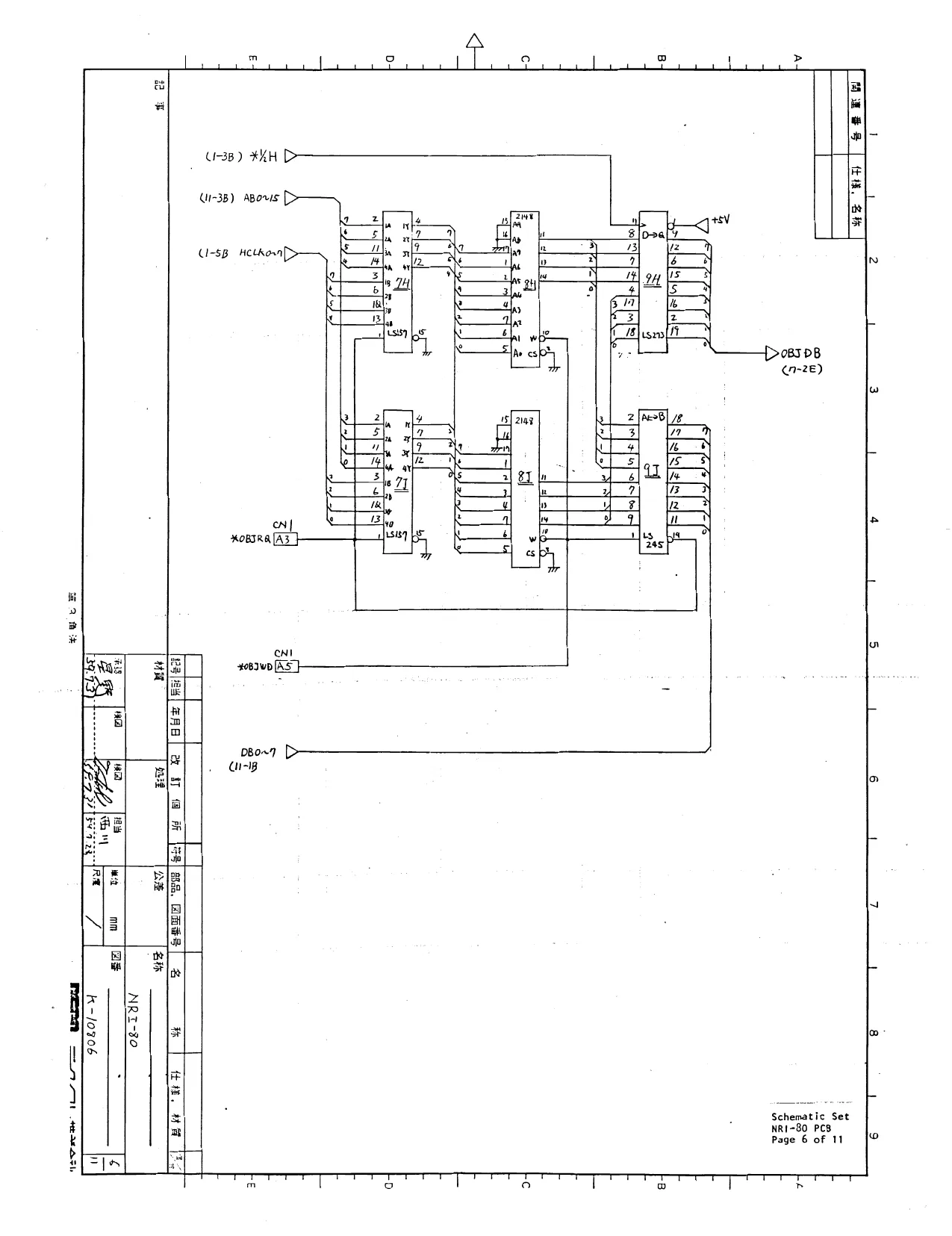
15 Schematic diagram - NANAO monitor 16 Schematic diagram - Sanwa Monitor 18+ Schematic Package - NOI-80 PCB (12 Pages) Schematic Package - NR!-80 PCB (11 Pages)
Schematic diagram for ASAHI! model 6352 power supply was not available for inclusion in this manual at press time, Refer any problems to the DATA EAST Service department.
Kara
Game
3. te Champ
instructions
Training Use this session to learn and to practice the various moves. You can enter directly into game play by pressing either 1 or 2 player start button.
Left Joystick controls player's direction of movement Right joystick controls player's choice of attack Both must be used together to execute the different moves.
MATCH
Maneuver YOUR PLAYER to fight against your opponent. Move joysticks to execute the various moves (see move chart) First fighter to score 2 points wins match Player advances to next level for each match won,
BONUS INTERVAL
After each match, play bonus rounds to score additonal points.
Page 1
KA RATE
CHAM P
LEVER INSTRUCTIONS
WHITE PLAYER
“rt PERONTRIGKT
| i | PBACK Kick | [= RIDELE | ROUND KICK | LOW KICK |
| Sit | cal | PUNCH |
WITHDRAW | > BACK ; : UPPER
| ——]| | BACK KICK | | FOUND | Low KICK. | ||
| i | sock. | |. | | | Kick | PUNCH |
i “|= CHANGE ~ | MIOOLE | UPPER LUNGE
| ! | FORWARD { DIRECTION [LUNGE PUNCH | | PUNCH | | LOW KICK |
i BACK KICK | FRONT KICK | ROUNO Kick | :
| | | -ghigies | AMPING | JUMPING | BACK WARD| FORWARD |
pos BACK KICK |. SIDE KICK | SOMERSAULT | SOMERSAULT “FOOT SQUATTING
| 2a | SWE | EER" | | LUNGE PUNCH |
RED PLAYER
MIDDLE
BACK KICK “REVERSE
| wo | i aes | ‘PUNCH, | ||
| WITHDRAW J 82 | BACK | F | ae | ; |
| BACK KICK | |__ ROUND | Pca | Low KICK | |
| BLOCK | eed | Kick | ICH | dacs |
| mr | *” CHANGE | MIDDLE.” | UPPER LUNGE | ~ | ||
| FORWARD. | |. DIRECTION |LUNGE PUNCH | PUNCH | LOW kick |
BACK KICK | FRONT KICK | RGUND KICK |
| UMP | JUMPING | JUMPING | BACK WARD} | FORWARD |
| J | oh BACK KICK | SIDE KICK | SOMERSAULT | SOMERSAULT |
- Teck Foot [Front root] SQUATTING |enony FOOT |
| SQUAT: | SWEEP | sweep | | REVERSE | sweep |
LUNGE PUNCH
Page 2
KARATE CHAMP
Player Vs Player
OPTION SWITCH SETTINGS
right coin acceptor on 4 OFF 1 coin | 1 coin 2 coin 3 coin sn tor 1 pla 2 a 1 play 1 ei ecep DIFFICULTY SETTING
FREE PLAY
Page 3
LAMP and SPEAKER PANEL (mounted behind marquee plex
8 Ohm Soeaker MARQUEE PLEX
MARQUEE PLEX RETAINER,
MONITOR PLEX
MONITOR
CONTROL PANEL
K CONTROL PANEL CLAMP
PCB and EMI SHIELD
COIN DOOR ASSY
» COIN COUNTER < I (in vault) - < VAULT CASHBOX (in vault) _ Fi i rss or POWER SUPPLY
Page 4
POWER SUPPLY REQUIREMENTS
| 5y | 42% | | | 5A |
| “+12v | 42% | | | 1A |
L. =
| —s5v | 42% | | | 0.14 |
OPERATING ENVIRONMENT
Temperature Humidity
Operation | 5~35° C 20~80%
| | | Storage | —15~65° C | 10~90% |
RASTER SCAN MONITOR SIGNALS
- Color Signals R-G.B. Separate
Black O- +2Vv
Image Signal +2.5v - +4V
- Syncronize Signal Composite
- 0 - 0.5V
1 43V - +5V
- Screen Image Size
Image can be shrunk both horizontally and vertically by 10%.
Page 5
KARATE CHAMP
Signal Assignment Table
Connector CR7E-44DA~-3.96H (HIROSE) ‘Terminal Numbering 223456 76 FR WON 12 BIS 1617 189.202) 22. jesaicce esis ft Cees o Sree = = ESSE SS O| irr if { SS (SlSiSilSisilais Sus lfSvevslfer= | o| =! oS
Signal Assignment A BCBEFHIKLMNPRSTUVWXYS
| Pin Nos | Pin Nos | Signal | |||||
| [2 | | i | Right | Up . | | “Bp | | 2P> _ Right Up | ||
| 3 | 1p | Right | Left | Cc | 2P | Right | Left |
| ap" | Right Right | |) eP Right 7 Right | |||||
| SP | nett Downs | PO | Let Down] | ||||
| Cr | cs os | rn | | | i | i | es as cc a | |
| 7 | | IP Lett | ‘Terft | «(| RK SC*Y Pett | Lett | |||
| “eT - Lett | “Right | oP | Left Right | |
GND. lo [ia ~~ Tp ‘Game Select ~~ 12 | Goin Switch 1
ee | W ne ee
ee —= aT
Page 6
COUNTER vec
‘coumTER
COUNTER
COIN 1
COIN 2
GND PCB DFV-01 COIN COUNTER CIRCUIT
DIODE
COIN COUNTER #2
NOTE: On some DIODE
games DN3-13 is jumpered to CN3-P.
COIN sw.
XX¥. NO COM. (jumper installed > on Coin Door) —* COIN sw 2
N.O com. oO
Page 7
at ia Spay FOE 864% so ROG ore:
Leygon ee CRS t+ fie ee] cH 4 Yet Vea” I P3iw waz Go “—
- @ sant Su ecpt
- NOT PROCEEDED. CR3L O31, C31, R32, R33 &&® SANKEN Sw§ -608
SWITCHING REGULATOR
This page reads as a drawing: its text was drawn rather than typeset, and comes out in fragments. See the original scan.
«
Item
.i.
2.
3.
4.
be 6.
Ts 8.
9.
lo.
ll.
12.
13.
14.
16.
17.
18.
19.
20.
21.
22.
23.
a4.
25.
26.
27. “28. Fao
Td4o
Q4o0
RF4o
Dido DA6
DZ40
ICol
PCol
C4o,
CAT
C80
c42
c43
C46 Parts Nos
4o , 46 Description
Fuse
Transformer
Commom Mode Choke
Transistor
Bridge Rectifier
Diode
Diode
Zener Diode
HB: IC
Photo Coupler
Seramic Capacitor
Seramic Capacitor
Seramic Capacitor
Film Capacitor
Film Capacitor
Film Capacitor
Filn. Capacitor
Wlectrode Capacitor
Resistor
Resistor
Resistor
Resistor “Metal Plate Resistor
Coil Resistor
Carbon Resistor
Carbon Resbbtor
Carbon Resistor
Carbon Resistor Specification
GHS' 5
UF327S: 602YERO
2803306 -
S3WB 4o
Vv1g9C
v19G: HZ16-1
RHDol1-2
PS 2018
DE7090B 1lo2KVAl 125 1,ooopf
- ditto -
D&o707B 681K 2Kv DC 68op
QEM2 G' 1o4kT 4oo¥ o-lpf ECQ-E2 104KS 200V. o. pt BCQ-E6 473KZ 4ooV' o O47 pt LJA2D471 THSCBV 200¥ ATopt ERG1SJ 3934,
ERG-2SJ 223Hi
ERG3S3- 560K
ERG+2S5 330H'
MPC Jo 0.22 ohm
» MNS o5N 1Rog: 1/4W 10K ohm 1/4 680 ohm 1/4W 12K ohm
Page 10 | PPP PP eB PP PPP
a
PRPPNHeHP DYDD Qtty Manufacturer
Negasawa Shindengen TDK
Toshiba
Shindengen Hitachii
Hitachi
Hitachi.
Nichi-com
- Nichiden(NEC) Murata
Murata
Murata
Nichi-con
Matsushita
Matsushita
Nichi-con
Matsushita
Matsushita
Matsushita
Matsushita
Fukushima Futaba
Microm
Item
29.
30.
3a.
32.
33.
34.
35. 36.
38.
39,
4o.
42.
43.
44.
45.
46.
AT. 48.
49.
50.
51.
52.
53. 54. 55. + 56. 57. 58. Parts Nos Description
Lol Choke
Lo3 Choke
go2 Transistor
Dol Diode
Do2 Diode
Bo3 Diode
DZ02 Zener Diode
DZo3 Zener Diode TIUYol Thyristor Ieo2 rec.
Col, o2 Capacitor
Co3, 05 Capacitor
Cod Capacitor
CoT, 06 Capacitor
Co8 Canecitor
Co? Capacitor
ell Film Capacitor
Rol, 13 Resistor
Ro8 Resistor
Rod Resistor
Rlo Resistor
RVol Volume
Ro3” Carbon Resistor Ro4, 11 Carbon Resistor Ro5 Carbon Resistor Ro6 Carbon Resistor Ro2 P.C. Board TB1l Terminal Strip Terminals RD1113A 30 1 3uH lof
RD81oA 3F 1 Bull 5A
28D1022 or 28D1308 1 BSAC 83-004 1
5CH2M or” ESAC25-020
- ditto -
HZ 6B-2
HZ 12B-1L
5PIM or SF5B41 TI431 CLP SXA 16VB 2200
CRUSM 1V: 47a 35V' 47opt CEUSH 1 331 1 25W 330pf CHUSH 1 331 2 25V 330pf CEUSM 1H*olo
CEUSM LV 4R7 1 35W 4.7pf TDYLH/2A loAK 1 Sow o.lpf ERG 38J' 6808
ERG3SS. 2710 ERG! 257 R68 2 0.68 ohm
ERG! 187 271 1 IW 27o ohm DMP RP PB
ny
EVN38GR. 500 ohm. 1/4 68 ohm 1/40 560 ohm 1/4W 390 ohm 1/4w 15 ohm ooB52 1
PREM HE
eR Faston
Page 11' Specification Qtty Manufacturer
Hokkoh
Hokkoh:
Shindengen
Fuji Denki Puji Denki or+NEC Fuji Denki
Hitachi
Hitachi
NEC or Toshiba
TT.
Nichi-Chemi
Wichi-con
Nichi-~con
Nichi-con
Nichi-con 5oW 1pf Nichi-con
Nichi-com
Matsushita 3W 689. Matsushita 3YW 27ToR Matsushita
Matsushita
Matsushita
Page 12 To
Florescent
Lamp
Tv
Erase
Ty KARATE CHAMP : Power
Power Supply revit
for units having
WELLS GARDNER TV MONITOR
Lamps
Switching Regulator PCB Power
To
Florescent
Lamp
TV
Erase
KARATE CHAMP.
Power Supply Circuit
for units having
NANAO or SANWA TV Monitor
Lamps
Page 13
Switching Regulator PCB Power
WOLINOH YaNQYv9 $7734 ezeuvn '980H 260A dWW ONAS wort
Page 14 aosoosz “eopasz 4N0 HOH 2ee0 SABO} WVYOVIC SILWWEHOS YOLINOW SAID YO10D wre ‘2020.
Leura rexruncat es cide | @-Naot—-z4 WoLtNow FONT oz}
Covnvn) rey 2000 ogttosz
ASVUI A.SSV Z2EPNOIS so | 2@gunois
This page reads as a drawing: its text was drawn rather than typeset, and comes out in fragments. See the original scan.
VANVS
C200LOd) §/M A 1HO
$l e/8 evu S$ Ol% ayyor
kK ety eo .-s ern WEESY TSH —AWA- XeESY Ise
7]
B907 DST EID
Sl id teu ort fanor
Katee vey BROTOSZ zd “SL era4 Clu eeu Uo
HSL ole uu se ars“ We > OlT igyxor
wu WS g90290ST No
(So) wd 7)
Page 17
This page reads as a drawing: its text was drawn rather than typeset, and comes out in fragments. See the original scan.
This page reads as a drawing: its text was drawn rather than typeset, and comes out in fragments. See the original scan.
Bee K
RIERA SL USA) «TORQ USA) FRO
USA) ew p— 4 SRR
GUS MF
-zAyaest | D>
- INO (YE)
{> *SUHORR (ne)
G38) (4-26)
# oD WY k | Bee [Relea
e RAB ASUNORST
oR-ION & “2598 |S:
DIPSwI 3 |s220 be NAtON CI-3E)
- *FLIP T
Schematic Set NOi-80 PCB Page 3 of 12
This page is a drawing, shown as the original scan.
This page reads as a drawing: its text was drawn rather than typeset, and comes out in fragments. See the original scan.
This page reads as a drawing: its text was drawn rather than typeset, and comes out in fragments. See the original scan.
This page reads as a drawing: its text was drawn rather than typeset, and comes out in fragments. See the original scan.
This page reads as a drawing: its text was drawn rather than typeset, and comes out in fragments. See the original scan.
This page reads as a drawing: its text was drawn rather than typeset, and comes out in fragments. See the original scan.
This page reads as a drawing: its text was drawn rather than typeset, and comes out in fragments. See the original scan.
EeCw
Se ee | ag Ez: Ar
- PLsw/ DET}
ND erst ULE €rHsulb (4-ZE )
cnt [as Ws | se ee |
P>xtPiswiy 4-2E)
«Prism LOSE
Alt #LPSWILQU-2E)
¢ % PISW RETF
ene % Pisw20(} -#THSUAR( -2E)
cnr & Plsw2 v CC
cnr —{>s1psu2p 4-36)
> #1Piswat4 -3E)
¥ rise LCT}
¥ wz RR {D>aeisw2e @ -3€)
a fer isw2r (4-28)
¥ pswl Dd [A > eTraswiD (4-3E)
*& prs v [ “ene —f>-stp2seiula -4€)
¥ peswy LCT wn D>xrPiswiL (4-48)
- pesw RCD +
cn, D> arrrsivrn e-“E)
# Bow Le} R [BRS | set sa
aay
id Cat {>#irzsu2 D 64-46)
#& peswey [FF
CN? Pew LDL} [>xipzsuay 46)
D> erpsweL (a -SE) a % PsARE TS
CAL (>arpswer A-SE)
HIP BEL (HSE) & fase {A}
ent % risee OO
ne [h ue
i # IN] Oy a Pariser WS)
#ICINT W-6F)
cnt # Cone [LN Zs
Cie INCU} Rice C4-bE)
on aH ad a aH
{iz} CoINc|
on iicerco2 [> (P] cones
Schematic Set NOT=80 PCB Page 11 of 12
This page reads as a drawing: its text was drawn rather than typeset, and comes out in fragments. See the original scan.
This page reads as a drawing: its text was drawn rather than typeset, and comes out in fragments. See the original scan.
This page reads as a drawing: its text was drawn rather than typeset, and comes out in fragments. See the original scan.
This page reads as a drawing: its text was drawn rather than typeset, and comes out in fragments. See the original scan.
This page reads as a drawing: its text was drawn rather than typeset, and comes out in fragments. See the original scan.
This page reads as a drawing: its text was drawn rather than typeset, and comes out in fragments. See the original scan.
This page is a drawing, shown as the original scan.
This page reads as a drawing: its text was drawn rather than typeset, and comes out in fragments. See the original scan.
This page reads as a drawing: its text was drawn rather than typeset, and comes out in fragments. See the original scan.
Ewes
LS ga ae eed x 2
G-28) > y30
a gescqa, [> (3-18) X0UsLD Pe —
aa ei | t Ewa) [> cesvbo (e~az)
H
- 24 fi we —T
Fj
ste = =
Ge
he ce 6A| 8A |z0n Drew [ame [atd4 | {> opti Uo-2E)
Bie cee a
uslie
Ei,
Schenatic Set NRI-80 PCB “Page 9 of 11
This page reads as a drawing: its text was drawn rather than typeset, and comes out in fragments. See the original scan.
This page reads as a drawing: its text was drawn rather than typeset, and comes out in fragments. See the original scan.
WARNING
Federal law provides severe civil and criminal penalties for the unauthorized reproduction, distribution, or exhibition of copyrighted audiovisual works and video games. The Federal Bureau of Investigation investigates allegations of criminal copyright infringement.